Article

Low-Damage Reactive Ion Etching of Nanoplasmonic Waveguides with Ultrathin Noble Metal Films

by
Alina A. Dobronosova
1,*,
Anton I. Ignatov
2,*,
Olga S. Sorokina
1,2,
Nikolay A. Orlikovskiy
1,2,
Michail Andronik
1,
Aleksey R. Matanin
1,2,
Kirill O. Buzaverov
2,
Daria A. Ezenkova
1,
Sergey A. Avdeev
2,
Dimitry A. Baklykov
1,2,
Vitaly V. Ryzhkov
1,2,
Aleksander M. Merzlikin
2,3,
Aleksander V. Baryshev
2,
Ilya A. Ryzhikov
1,3 and
Ilya A. Rodionov
1,2
1
FMN Laboratory, Bauman Moscow State Technical University, Moscow 105005, Russia
2
Dukhov Automatics Research Institute, (VNIIA), Moscow 127055, Russia
3
Institute for Theoretical and Applied Electromagnetics RAS, Moscow 125412, Russia
*
Authors to whom correspondence should be addressed.
Appl. Sci. 2019, 9(20), 4441; https://doi.org/10.3390/app9204441
Submission received: 25 September 2019 / Revised: 13 October 2019 / Accepted: 15 October 2019 / Published: 19 October 2019
(This article belongs to the Special Issue Light Matter Interaction at Nanoscale: What Matters Most)

Abstract

:
Nanoplasmonic waveguides utilizing surface plasmon polaritons (SPPs) propagation have been investigated for more than 15 years and are now well understood. Many researchers make their efforts to find the best ways of using light and overcoming the speed limit of integrated circuits by means of SPPs. Here, we introduce the simulation results and fabrication technology of dielectric-metal-dielectric long-range nanoplasmonic waveguides, which consists of a multilayer stack based on ultrathin noble metals in between alumina thin films. Various waveguide topologies are simulated to optimize all the geometric and multilayer stack parameters. We demonstrate the calculated propagation length of Lprop = 0.27 mm at the 785 nm wavelength for the Al2O3/Ag/Al2O3 waveguides. In addition, we numerically show the possibility to eliminate signal cross-talks (less than 0.01%) between two crossed waveguides. One of the key technology issues of such waveguides’ nanofabrication is a dry, low-damage-etching of a multilayer stack with extremely sensitive ultrathin metals. In this paper, we propose the fabrication process flow, which provides both dry etching of Al2O3/Au(Ag)/Al2O3 waveguides nanostructures with high aspect ratios and non-damage ultrathin metal films patterning. We believe that the proposed design and fabrication process flow provides new opportunities in next-generation photonic interconnects, plasmonic nanocircuitry, quantum optics and biosensors.

1. Introduction

The semiconductor technology based on modern electronic integrated circuits is rapidly approaching their fundamental limits in terms of further transistors scaling and nanoscale elements’ thermal budget. In addition, the electrical signal transmission rate between various elements limits the interconnects performance. One of the alternative technologies that could overcome the existing limitations and ensure further performance growth is optical interconnects (including plasmonic) [1]. The high optical frequency allows for dramatically increasing information transmission and processing rates. At the moment, there are two main approaches to optical interconnects design for a system in housing: multiplexed interconnects (where different optical signals are transmitted at individual frequencies using one common optical waveguide [2]) and non-multiplexed interconnects (where signals from each source are transmitted via individual optical waveguides [3]).
One of the first implementations of optical interconnects was a rather cumbersome multiplexed scheme, proposed in 2001 by Miller’s group [4]. In modern multiplexed optical interconnect schemes [5,6], all bulky elements which connect waveguides and electronic microcircuits are replaced with dielectric waveguides and a dielectric multiplexer. Lens-free input/output systems based on integrated diffraction gratings were developed for optical waveguide coupling. However, despite the great progress in this field, the multiplexed scheme has a number of fundamental shortcomings. Firstly, diffraction grating-based input and output systems are speed-limited because of an increase in the transmission band leading to a decrease in power efficiency (growing scattering losses). Secondly, for the purpose of multiplexing signals from several sources, high-quality resonators are required. At the same time, excessively high-quality factors result in unfavorably high sensitivity to all the external influences, leading to signal modulation rate restriction (which is inversely proportional to the quality factor). On the other hand, the quality factor must be high enough to provide the entire frequency band separation into a row of separate channels.
Keeping in mind the existing drawbacks of multiplexed schemes, a number of scientific groups proposed schemes without multiplexing. In particular, in Reference [3], the scheme based on plasmonic waveguides was presented. The main shortcoming of the design presented in Reference [3] is the extreme technological realization difficulty required for fabricating parallel data transmission lines, which implies the same sequence of outputs on the driving integrated circuit chip and inputs on the receiving integrated circuit chip. In practice, this condition is not met and usually, a comprehensive multilayer wiring (more than ten physical layers) is needed to ensure a layout of transmission lines without any intersections. The concept of interconnects without multiplexing was further developed in the European research project NAVOLCHI (Nanoscale Disruptive Silicon-Plasmonic Platform for Chip-to-Chip Interconnection) (Figure 1a) [7,8,9]. It was devoted to the development of a nanoscale plasmonic chip-to-chip and system-in-package interconnection platform, including integrated nanoscale light sources and photodetectors. The goal was to combine nanolasers with an operating wavelength of 1550 nm [10] and plasmonic modulators [8,9] with silicon and polymer optical waveguides. In this project, signals from each nanolaser are transmitted using an individual waveguide to an individual photodetector. However, the technology of on-chip nanolasers [10,11,12] is insufficiently developed, therefore, their practical implementation is complicated.
Taking into account the drawbacks of multiplexed schemes, we consider in this paper the scheme without multiplexing. Opposite to the approach used in Reference [3], we assume the possibility of waveguides crossings and, unlike the NAVOLCHI project, we focus on well-developed miniature lasers suitable for mass production—vertical cavity surface-emitting lasers (VCSELs). It is worth noticing, that commercially available VCSELs are already supporting data transmission rates up to 25 Gbit/s in a wide temperature range from 25 to 85 °C [13]. The proposed interconnects scheme is shown in Figure 1b. The basis for the proposed interconnects is the plasmonic data transmission line–plasmonic waveguide combined with in- and out-coupling structures (input/output diffraction gratings). We outline that such waveguides must support propagation of a plasmonic guided mode over sufficiently large distances and have low scattering loss at waveguides intersections. We demonstrated in the paper below (see Section 3), that the waveguides with numerically optimized parameters meet both the requirements simultaneously. We consider plasmonic waveguides due to its ability to support sufficiently long mode propagation distances, possibility to integrate plasmonic waveguides with electrical contacts of active photonic devices in a natural way [14]. In addition, plasmonic waveguides have the potential of using elements of optical chemical, bio and other sensors due to strong field enhancement near metal waveguide elements [15,16].
The typical chip-to-chip interconnect length for a system in housing is about 1 mm. In the case of plasmonic waveguides, such a propagation length is achievable only for the so-called LR-DLSPPWs (long-range dielectric-loaded surface plasmon-polariton waveguides), which we consider in this paper. The long-range plasmonic mode propagates along a thin metal film (about 10–20 nm thick) [17,18,19,20], with materials of the same dielectric permittivity on both sides of the film. Since for practical use the plasmonic waveguide must be fabricated on a rigid optically transparent substrate, quartz is usually chosen as such a substrate. To match the dielectric permittivity, the thin metal film can be coated from its upper side with liquid saline solution [21]. By changing the salt concentration, the solution dielectric permittivity can be precisely matched to the substrate’s one. An alternative approach is to fabricate an intermediate layer (between the substrate and the metal film) with low dielectric permittivity and deposit a high-dielectric-permittivity layer atop the metal film. Both approaches are not easy-to-use in term of interconnects fabrication, as they require specific materials which are not used in the electronics industry.
In our paper, we propose plasmonic long-range waveguides with the widely used material, Al2O3, as a high-index dielectric. To fabricate multilayer Al2O3-metal structures, a technological process was developed that includes the following basic operations: deposition of thin-film functional layers, e-beam lithography and dry plasma-chemical etching. One of the most critical technology issues of the dielectric-metal-dielectric long-range nanoplasmonic waveguides fabrication is low-damage plasma-chemical etching. The fact is, that the defined stack materials (Al2O3/Au(Ag)/Al2O3) require both contradicting etch recipe parameters and gas mixtures, which lead to degradation of ultrathin metal films. The optical and plasmonic properties of thin noble metal films and the mechanisms of their degradation are well studied [22,23,24,25]. In our paper, a multistage and precise process of dry plasma-chemical etching is proposed, which ensures reproducible etching of the multilayer waveguide nanostructures and eliminates the degradation of their optical (plasmonic) properties.

2. Materials and Methods

Multilayer waveguide thin film stacks were deposited on prime-grade quartz substrates (Siegert, Germany) using a 10 kW e-beam evaporator (EvoVac, Angstrom Engineering, Canada) with a base vacuum lower than 3 × 10⁻⁸ Torr. We first cleaned the quartz substrates in megasound deionized water (DIW), followed by a 4:1 sulfuric acid and hydrogen peroxide solution at 80 °C, followed by further cleaning in isopropanol to eliminate organics. Then, we immediately transferred the substrates into the e-beam evaporator chamber and pumped down the system to the base vacuum. All the films were grown using 5N (99.999%) pure silver and gold pellets, 4N (99.99%) pure aluminum pellets, 3.5N (99.95%) pure tungsten pellets and silicon dioxide tablets (99.99%). The films were e-beam evaporated in the same vacuum cycle with rates of 2–10 Å·s−1 measured with quartz monitor at an approximate source to substrate distance of 30 cm.
Multilayer waveguide topology was patterned by electron beam lithography (EBL) followed by reactive ion etching. The EBL process started from e-beam resist polymethyl methacrylate (PMMA) A4 (MicroChem, Westborough, MA, USA) spin-coating (Brewer science, Rolla, MO, USA) on square quartz substrates (25 × 25 mm size) with a spin speed in the range between 1200–2000 rpm for 120 s, and baked at 150 °C for 5 min. The EBL exposure dose was between 450–495 μC/cm2 depending on the topology element, with dimensions varying in the 0.3–10 μm range. Finally, we developed the samples after exposure in the MIBK (methyl isobutyl ketone) for 60 s. Next, plasmonic waveguide nanostructures were etched (Oxford Instruments Plasma Technology (OPT) Plasma Pro, London, UK) using the inductively coupled plasma-reactive ion etching process (ICP-RIE) in the BCl3-based plasma for alumina layers and Ar-based plasma for metal layers.
The film thickness was measured independently by scanning electron microscopy (SEM) cross-section and profilometry. Zeiss Merlin with a Gemini II column and energy-dispersive X-ray spectroscopy (EDX, Oxford Instruments, High Wycombe, UK) was used for topology critical dimensions measurements. All the SEM cross-section images were done after a standard substrate cleaving procedure. All the deposited films’ roughness and topography were measured by stylus profiler KLA Tencor P17 (with Durasharp 38 nm tip radius stylus). All the measurements were done using 0.5 mg taping strength, a 2 μm·s-1 scan rate and a 20 μm scanned line length. In order to check the quality and uniformity of the deposited thin films, the surfaces after deposition were investigated by means of a scanning electron microscope. All SEM images were obtained using an in-lens detector and the accelerating voltage 1–5 kV and working distance from the sample to detector from 1 to 4 mm. Magnifications 3000, 7000, 15,000 and 50,000 were used to fully analyze samples.

3. Results and Discussion

3.1. Long-Range Dielectric-Loaded Surface Plasmon-Polariton Waveguides (LR-DLSPPW) Simulation and Analysis

The considered plasmonic transmission line consists of a waveguide and light input/output diffraction grating. We considered two types of the waveguide cross-section with both silver and gold metal layers. However, in the paper we demonstrate only gold-based waveguides simulation results. For the first type, the lower Al2O3 layer has the same width (Figure 2a) as the upper one, while for the second type, the lower layer has a much larger (infinite) width (Figure 2b). The two Al2O3 layers’ thicknesses were optimized in order to maximize the long-range plasmonic mode propagation length while keeping a sufficiently large long-range mode effective index compared with the substrate refractive index (to avoid too-large scattering losses into the substrate on waveguide roughness and bends). The Au layer thickness was taken to be 8–12 nm, which is a reliable technological minimum for continuous films. Then, for the optimized thicknesses of the three layers on the substrate, the waveguide width (the width of the three-layer Al2O3/Au/Al2O3 or the two-layer Au/Al2O3 strip) was optimized in order to maximize the long-range waveguide plasmonic mode propagation length while keeping the waveguide to be single-mode (having only one long-range guided mode). Figure 2c shows the dependences of the effective index of the long-range mode in the infinitely wide three-layer system Al2O3/Au/Al2O3 on the upper Al2O3 thickness for different lower Al2O3 layer thicknesses. In Figure 2d, the corresponding dependences of the long-range plasmon propagation length are presented. All calculations are given for the wavelength of 785 nm.
Based on the results presented in Figure 2, the thicknesses d1 and d3 were chosen so that the plasmon effective refractive index exceeded the substrate refractive index by more than 0.05, but the plasmon propagation length was maximal. This requirement approximately corresponds to d1 = 75 nm and the maximum of the corresponding curve in Figure 2d, i.e., d3 = 240 nm. In such structures, the calculated long-range plasmon propagation length is Lprop = 0.27 mm for the wavelengths of 785 nm.
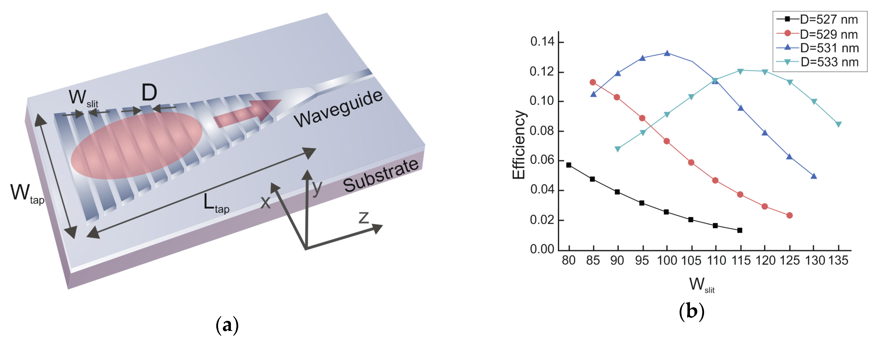
As in/outcoupling systems for light, we considered tapers with periodic gratings of slits cut through the two upper layers of the three-layer Al2O3/Au/Al2O3 (see Figure 3). The tapers are made from three-layers Al2O3/Au/Al2O3 with the same layer thicknesses as in the LR-DLSPPW waveguides, which makes it possible to fabricate it in the same process steps. The tapers focus the long-range plasmonic waves into the LR-DLSPPW aperture. In turn, to excite long-range plasmonic waves in the taper by an incident Gaussian beam, a periodic grating of slits in the taper is used.
To select the optimal parameters of taper with the grating of slits, we first optimized the parameters of a grating in the three-layer Al2O3/Au/Al2O3 of infinite width (two-dimensional (2D) grating), and then we optimized the taper opening angle, the taper length Ltap and the distance from the grating to the taper-waveguide junction. As the exciting wave, we considered a Gaussian beam with a waist width of w0 = 8.5 µm, normally incident from the substrate (the focus is located at the substrate-Al2O3-layer interface). The grating period, D, and the slits width, Wslit, were varied in order to maximize the efficiency of the long-range wave excitation in a 2D layered system. Optimization was performed with respect according to the lattice period, D, and the width of the slots. The case of a 2D exciting Gaussian beam was considered (the waist is w0 in the yz-plane perpendicular to the slits direction and is infinite in the x-direction along the slits). The number of slits was taken to be N = 38. For such N, the grating length is approximately equal to 20 μm (or 2.3w0) for the grating period D = 531 nm. In Figure 3, the 2D grating efficiency (calculated as a ratio of the long-range plasmon power excited in the +z direction in the layered system of infinite width to the incident 2D Gaussian beam power) as a function of Wslit, and D are shown.
As we can see from Figure 3b, the highest grating efficiency is observed at D = 531 nm and is about 13%. The taper width, Wtap, should be several times larger than the exciting Gaussian beam waist, w0. For example, we take Wtap = 30 μm. The taper opening angle θ (determined by the ratio W t a p / L t a p ) should approximately meet the condition:
W t a p / 2 L t a p = tg θ 2 = ( n e f f s u r f ) 2 ( n e f f ) 2 n e f f s u r f
where, n e f f s u r f is the real part of the long-range plasmon effective refractive index in the three-layer Al2O3/Au/Al2O3 system on the substrate and n’eff is the real part of the long-range plasmonic mode of the LR-DLSPPW of finite width. This condition determines the maximal angle θ/2 of a taper long-range plasmonic wave incidence for which this plasmonic wave could be coupled into the LR-DLSPPW. For a larger θ, however, the reflection of the long-range modes of the taper from the taper-waveguide junction is too large. Thus, we obtain Ltap = 100 µm. Note also, that at a crossing of two presented waveguides, there is practically no energy transfer from one waveguide to the crossing one (less than 0.01% of power).
In Figure 4, the electric field amplitude distribution is shown for a long-range plasmonic mode incident on a crossing of two LR-DLSPPWs. Three-dimensional finite element calculation gives a power transmission coefficient of 94% for a long-range plasmonic waveguide mode, a power reflection coefficient back into a long-range mode and a scattering coefficient into long-range modes of the perpendicular waveguide to be less than 0.01% in power.

3.2. LR-DLSPPW Fabrication Process Flow and Key Issues

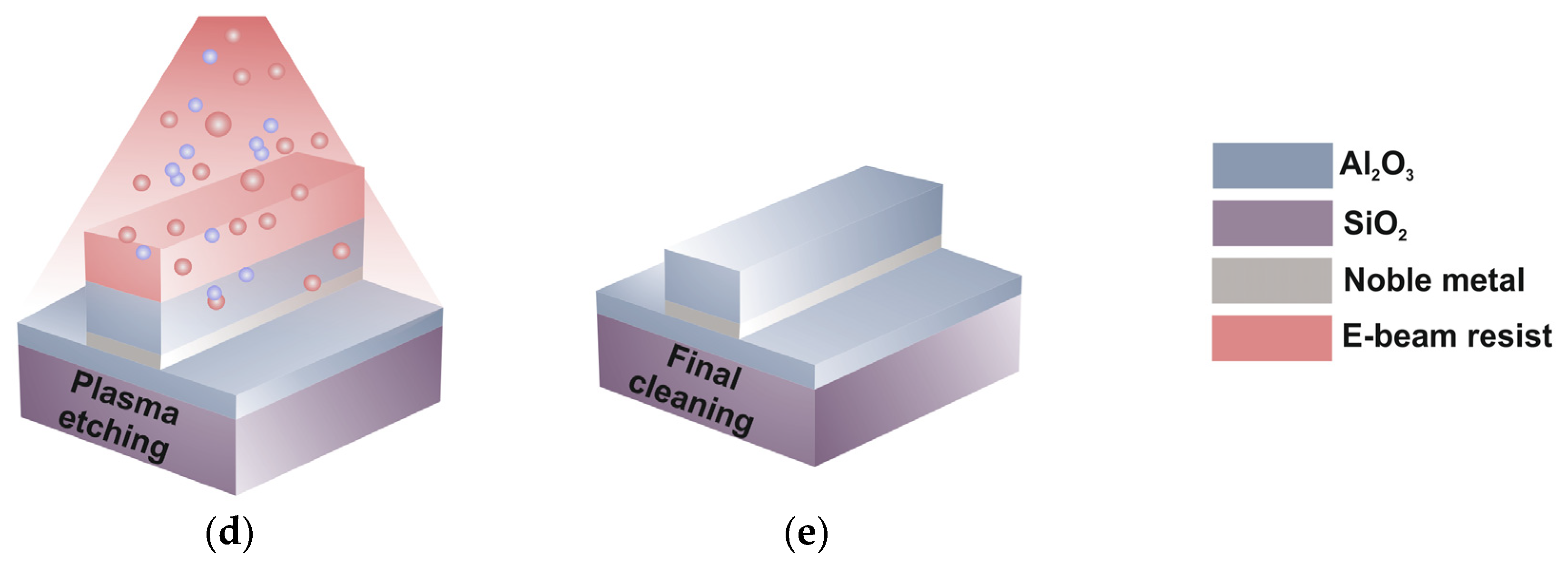
The general fabrication process flow for Al2O3/Au(Ag)/Al2O3 plasmonic LR-DLSPP waveguides on a quartz substrate is illustrated in Figure 5. The process begins with substrate surface wet cleaning using megasound particle removal in DIW, followed by 80 ˚C Piranha solution and drying with nitrogen (Figure 5a). Next, a three-layer thin film stack Al2O3/Au(Ag)/Al2O3 is e-beam evaporated in the same high vacuum cycle (base vacuum 3 × 10⁻⁸ Torr.) with both in-situ quartz and optical thickness monitors to ensure accurate and reproductive film thicknesses (Figure 5b). If hard masks are used for following the dry etch steps, then hard mask thin film is deposited together with the main three-layer thin film stack. Then, it is coated with a conventional e-beam resist and mask-less e-beam lithography is employed to expose a latent image of the waveguide topology in the resist layer. The e-beam lithography is completed (Figure 5c) with a wet development that reduced the resist to a uniform topology of waveguides (interconnects or plasmonic nanocircuitry). In case of the resist mask, these topology elements serve as a mask during an ICP dry etch process that transfers the photoresist image into the Al2O3/Au(Ag)/Al2O3 plasmonic LR-DLSPP waveguides. In case of a hard mask, these topology elements serve as a mask during a hard mask ICP dry etch process followed by a second ICP dry etch (Figure 5d) process that transfers the hard mask topology into the Al2O3/Au(Ag)/Al2O3 plasmonic LR-DLSPP waveguides. A final stage cleaning process (Figure 5e) removes any residual photoresist, hard mask or contaminants from the etch plasma.
One of the most challenging processes of the proposed fabrication process flow is a low-damage reactive ion etching of a multilayer dielectric/metal/dielectric stack with ultrathin noble metal films, especially in cases of ultra-hard dielectrics like alumina due to a number of contradicting technological requirements. On the one hand, dry etching of a waveguide stack top alumina layer requires aggressive chlorine-based etching gasses and high process power as the result of natural alumina hardness and low etching speed. On the other hand, chlorine-based etching chemistry usually leads to intensive reaction (plasma/thermally stimulated) with complete degradation of ultrathin noble metal films. The widely used BCl3-based alumina etching process was chosen to ensure high selectivity patterning of plasmonic LR-DLSPP waveguides nanostructures (due to efficient oxygen extraction in the form of BClxOy components [26], which then are decomposed by plasma and chemically react with both components of Al2O3 oxide):
2BCl3+ 3O → B2O3 + 6Cl
2Cl + Al → AlCl2
Two main gas phase and volatile reaction products (AlCl2 and BOCl) are finally formed, which could be easily removed from the etching reaction zone during the process. To provide high selectivity and etching speed, the process is usually carried out in inductively coupled plasma (ICP) etching mode at relatively high ICP generator power (~1000–2000 W). However, such high-energy processes with aggressive (corrosive) etching gasses in most cases result in underlying ultrathin metal films damage because of both thermal and chemical influence (
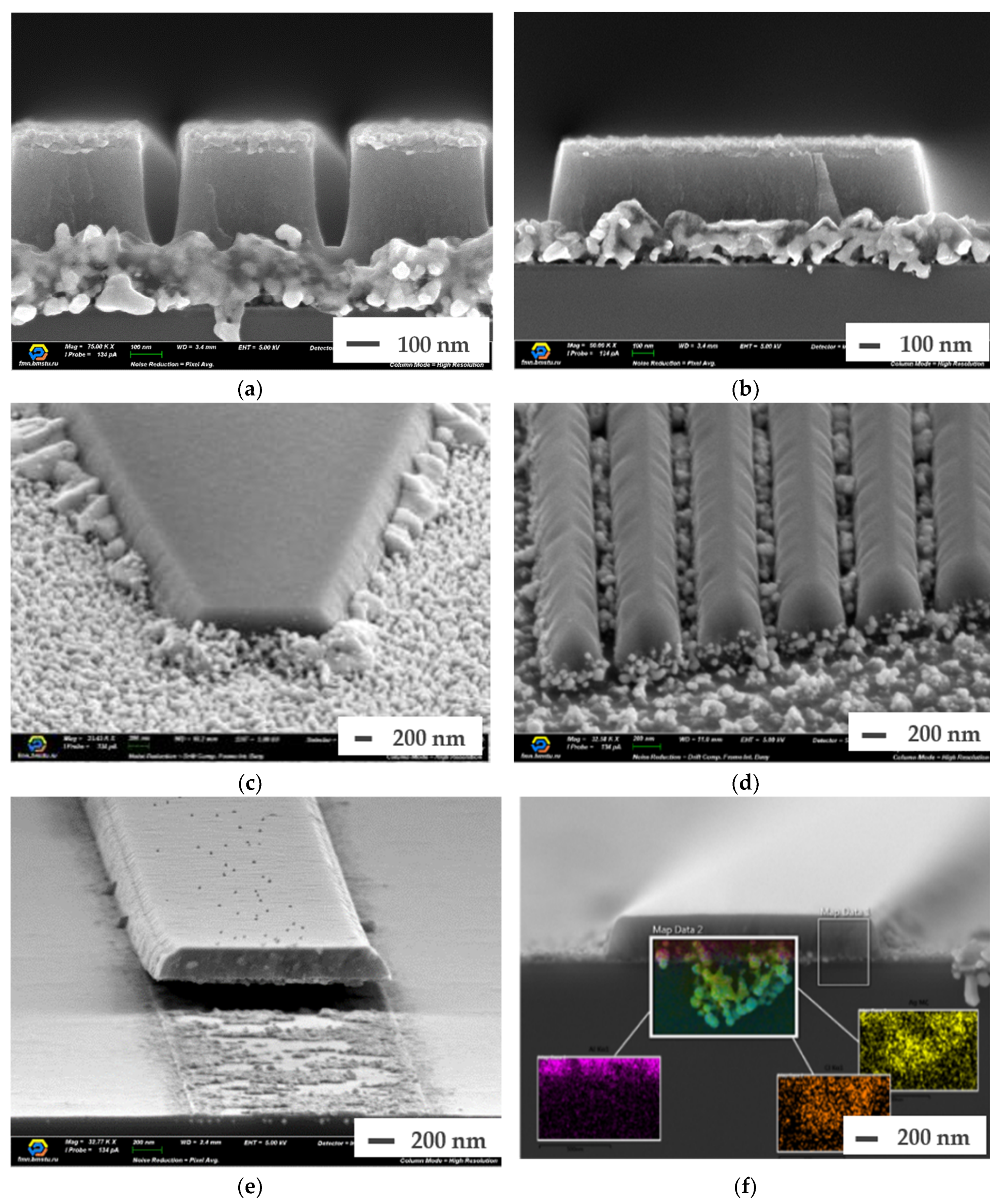
Figure 6). Figure 6a, b demonstrates the Al2O3/Ag/Al2O3 waveguide cross-sections with completely destructed silver ultrathin film inside because of overheating, only when the upper Al2O3 layer has been partly etched (70% of its thickness) and there was no interaction of etching gasses with silver films. The examples of the complex chemical reactions (with silver chloride products formation due to combined plasma/temperature action) of etching gasses and waveguide stack thin films are shown in Figure 6c–e, when the Al2O3/Ag/Al2O3 stack was etched through to the substrate. It is worth noticing, that due to the micron overall dimensions, entire ultrathin metals inside waveguides are usually damaged (Figure 6e) during the etching process, leading to complete plasmonic properties degradation.
We experimentally observed the active interaction of BCl3 with silver thin films during the top Al2O3 layer etching with the non-volatile chemical products formation and its redeposition on the resistive mask (Figure 6c–f). Additionally, these redeposited products mask the main waveguide micro- and nano-structures, and result in an uncontrolled, nonreproducible etching process. Moreover, when silver and top alumina layers are etched in the same BCl3-based process, micro- and nano-particles reaction products (Figure 6c,d) are formed on the etched surfaces, which could not then be selectively removed. The chemical reactions of particle formation in BCl3 plasma and a possible solid precipitation reaction are presented below:
e2- + BCl3→ BCl2 + Cl-
e- + BCl3→ BCl + Cl2-
e- + BCl→ B + Cl-
Ag + Cl-→ AgCl (s)
We confirmed this hypothesis using SEM EDX analysis of waveguide cross-sections (Figure 6f), demonstrating AgxClx- and Cl-based reaction products [27] in the degraded silver film. To completely eliminate chemical degradation of LR-DLSPP waveguides ultrathin silver films, the etching process should be carried out using chemically inactive gasses like Ar, He or H2 [19].
In contrast to silver, gold thin films dry etching in chlorine gasses could be very effective due to stable volatile reaction products (Au2Cl6) formation, which allows efficient removal of reaction products from the etching area. Additionally, it allows for providing high etching rates (approximately 350 nm/min) and minimizing material redeposition on the sidewalls of the resistive mask. By using chlorine-based etching processes, a good balance between the etching rate and profile could be achieved by optimizing recipe parameters. When using neutral etching gasses such as H2, He and Ar, the physical sputtering process predominates, which drastically reduces etching selectivity. It is worth noticing, that for gold etching with hydrogen, the chemical reaction also takes place, since AuH and AuH2 reaction products are formed, but its contribution is insignificant. These reaction products have low thermodynamic stability, which can also lead to the formation of redeposition defects on the sidewalls of the resistive mask. Furthermore, gold etching based on H2, He and Ar gasses results in weak gold film etching rates, which are 3–5 times lower compared to chlorine-based processes [28].
The multi-step high-precision dry etching process is developed to provide high-quality waveguide stack etching, eliminate reaction products formation and redeposition, and prevent overheating of ultrathin metal films. At the first stage of the process, 90% of the top alumina layer is selectively etched in chlorine gasses, leaving around 10–25 nm of alumina above the metal layer. This process ensures to eliminate the contact of the metal film with chlorine gasses. At the same time, it provides selective etching of the main thickness of the top thick alumina layer and ensures perfect quality of waveguide nanostructures with a high aspect ratio. Then, the residue alumina 10–25 nm layer and metal thin film have to be etched. We observed that during the etching process, due to surface bombardment and ongoing chemical reactions, the surface temperature of the samples rises above 75 °C, which is one of the reasons for structural changes in metal layers. To prevent overheating of metal films, we tested two methods: pre-cooling the samples before the etching process and stopping the etching in the middle of the process for intermediate cooling. It can be noted that prior cooling of the samples to minus 20 °C before the etching process can significantly reduce overheating and structural changes in the metal film (Figure 7b), but it does not completely solve this problem.
The second technological issue in the fabrication of the proposed waveguides design in is low-damage reactive ion etching of Al2O3/Ag(Au)/Al2O3 high aspect ratio nanostructures. The Al2O3 etch selectivity to majority standard electron resists (PMMA-like) in chlorine gasses is usually from 1:10 to 1:1 [29]. In the proposed waveguide design, the top alumina layer is around 250 nm thick, with the 100 nm sized topological elements critical dimensions. Taking into account Al2O
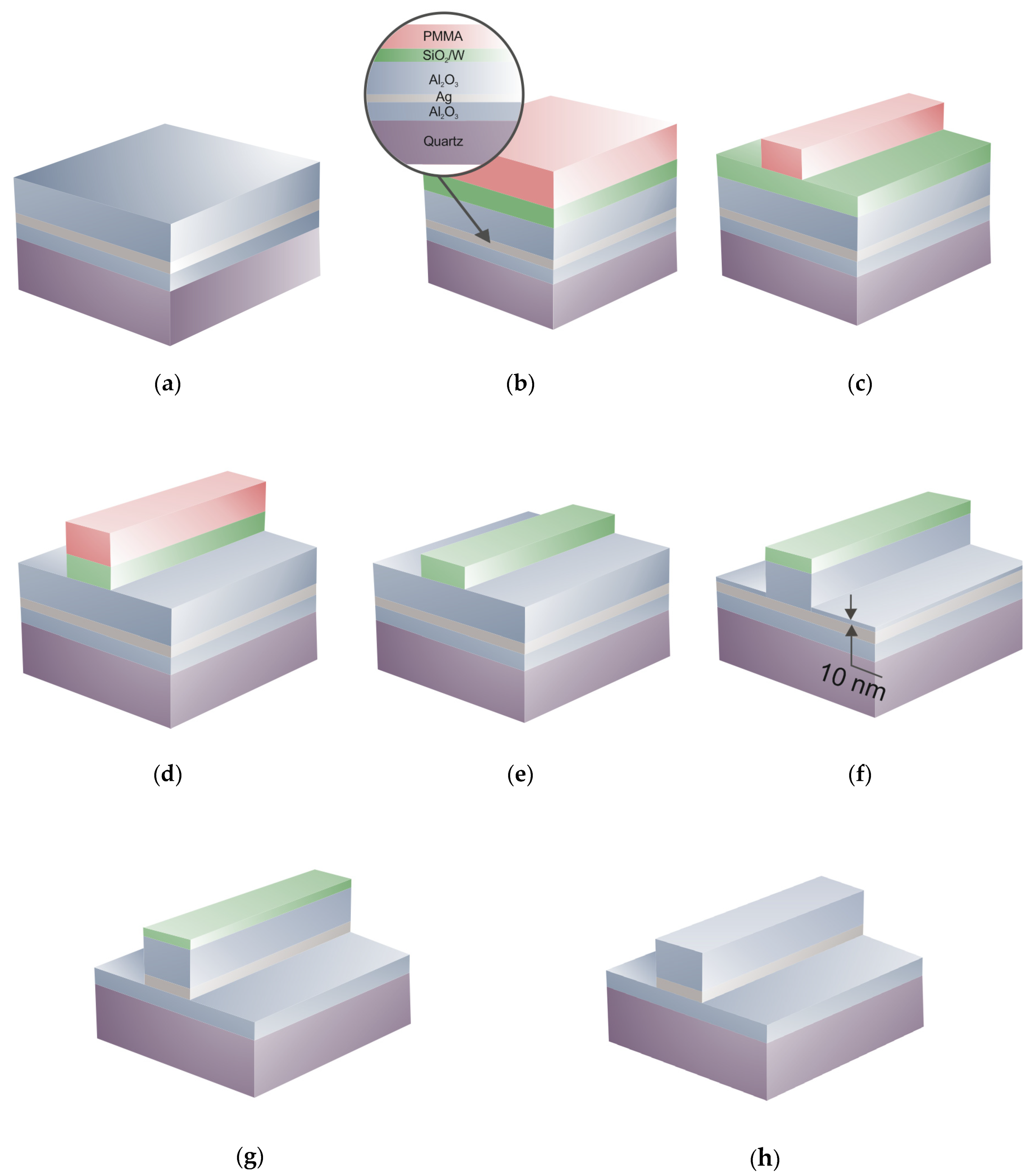
3/PMMA etch selectivity, the 750–2500 nm thick resist mask is required to provide high-quality 100 nm features etching. In this case, the aspect ratio for the e-beam lithography process varies from 1:7.5 to 1:25, which is an extremely difficult task for standard PMMA-like resists and 50/100 kV e-beam tool. Moreover, dry plasma etching through the PMMA mask with such an aspect ratio is practically impossible due to extremely limited access of the etching reagents and further reaction products removal. That is why, in this paper, we compared the PMMA mask to silicon dioxide and tungsten hard masks (Figure 8), which have better selectivity and can be selectively removed after the etching process from the Al2O3 surface.
After the first set of experiments, we concluded that PMMA masks are not suitable for the proposed waveguide design fabrication due to very low PMMA selectivity in chlorine gasses. The experimentally measured etch selectivity of silicon oxide hard masks in BCl3 gasses to alumina was from 1.5:1 to 1.7:1, depending on the process recipe. In order to etch through the simulated Al2O3/Ag(Au)/Al2O3 (75–12–240 nm) stack, we developed the process of 500 nm thick (taking into account required over-etch) silicon oxide hard mask fabrication using standard plasma-enhanced chemical vapor deposition (PECVD), e-beam litho and ICP dry etch process flow. We observe that high-quality waveguide topologies could be nanofabricated using the proposed low-damage dry etching process. Unfortunately, the silicon oxide hard mask final removal process became the insurmountable problem. Dry etch removal leads to plasmonic metals damage, while both wet hydrogen fluoride (HF):DIW (1:100, 1:50) and vapor HF methods result in plasmonic metal adhesion failure to the bottom alumina layer (Figure 9b–c). Nevertheless, we consider that further silicon oxide hard mask removal recipe optimization (HF:DIW concentration and vapor HF etching recipe) may allow us to successfully finish the waveguide fabrication process.
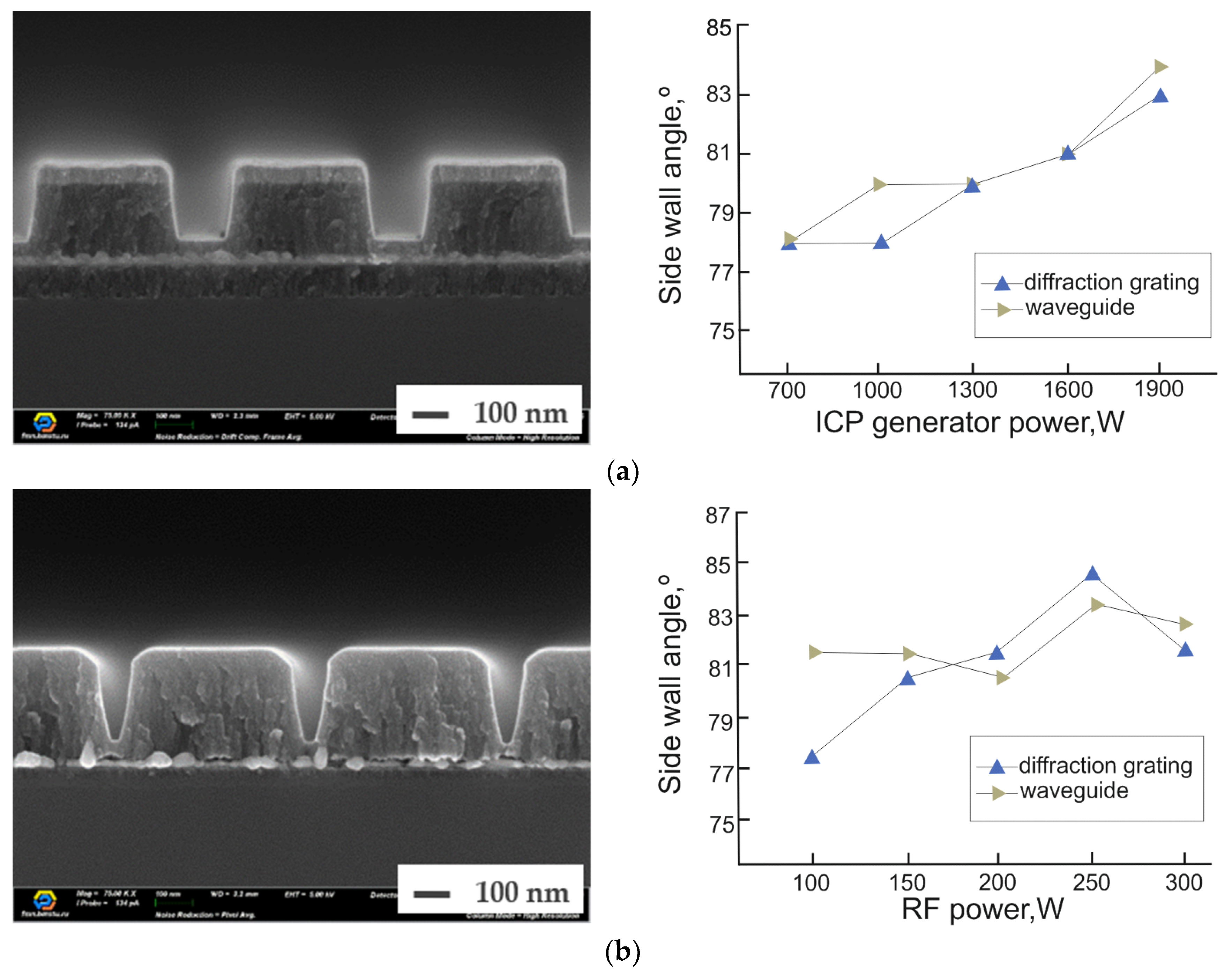
The experimentally measured etch selectivity of tungsten hard mask in BCl3 gasses to alumina is relatively high, 3:1, which makes it possible to use a significantly smaller thickness of the tungsten hard mask as compared to silicon oxide. Therefore, thinner hard masks could be used, which results in better e-beam lithography resolution and reduced aspect ratio, which improved access of etching reagents and reaction products removal. As the result, a 140 nm thick tungsten hard mask is required to etch through the simulated Al2O3/Ag (Au)/Al2O3 (75–12–240 nm) waveguide stack.

3.3. Al2O3/Ag (Au)/Al2O3 Dry Etching Process

The developed low-damage reactive ion etching of multilayer plasmonic waveguides with ultrathin noble metal films consists of multiple steps and uses tungsten hard masks. The whole process starts from hard mask etching which assumes the etching pause during the process to cooldown and protect the ultrathin metal film from thermal degradation. Next, the first 240 nm thick Al2O3 layer (Al2O3/Au(Ag)/Al2O3) is selectively etched using the BCl3-based process for the depth of approximately 225 nm. The second step allows for both eliminating metal degradation due to chemical reactions of metal with etching gasses and providing an opportunity to selectively etch the major part of the hard Al2O3/Ag (Au)/Al2O3 stack. As mentioned above, thinner tungsten hard mask (compared to silicon oxide and PMMA) and etch recipe optimization allows for fabricating high-quality waveguide topologies with the typical 100 nm sized features (Figure 10).
In the next process step, the tungsten hard mask is removed using the standard CF4-based dry etching high-selectivity (>10:1) process, eliminating the possibility of Al2O3 waveguide structures damage. Finally, the residue Al2O3/Ag(Au)/Al2O3 waveguide stack, including the ultrathin plasmonic metal layer, is etched using the physical Ar-sputtering process (without tungsten hard mask) (Figure 11).
In order to take into account the top Al2O3 oxide layer thinning during the Ar-sputtering process, we deposit a thicker top layer of the initial three layer Al2O3/Ag (Au)/Al2O3 stack. At the final process stage, all the chlorine and fluorine residues have to be removed from the fabricated waveguide nanostructures and the substrate open areas. It can be effectively done by treating the samples in deionized water from 1 to 2 minutes immediately after the etching process [27]. The proposed process allows for eliminating ultrathin plasmonic films degradation, which usually actively interact with aggressive chlorine-based gasses and ensure a high quality LR-DLSPP waveguide nanostructures fabrication of on quartz substrates (Figure 11).

4. Conclusions

In conclusion, we developed design and fabrication technology of the long-range dielectric-loaded surface plasmon-polariton waveguides. First, we considered and numerically optimized various multilayer nanoplasmonic waveguides with silver and gold ultrathin films in between two Al2O3 dielectric layers on a quartz substrate. For the optimized thicknesses of the three layers on the substrate, the waveguide topology was optimized to maximize the long-range waveguide plasmonic mode propagation length while keeping the waveguide to be a single mode. We numerically demonstrated that the Al2O3/Ag/Al2O3 LR-DLSPP waveguide calculated long-range plasmon propagation length could achieve Lprop = 0.27 mm for the 785 nm wavelength. Then, the waveguide input/output diffraction gratings design was developed, and its parameters were numerically optimized, providing the calculated gratings efficiency over 13%. In addition, it was numerically shown that the intersection of such waveguides in the plane at right angles ensures the negligible signals crosstalk (less than 0.01%), that allows planar wiring of a complex integrated optical scheme (see Figure 1) without using multilayer wiring.
Unless it has very high and time-stable properties, the Al2O3 is a well-known natural, hardly treated material, in particular, in combination with ultrathin metal films in stack. In the paper we proposed the fabrication process flow (Figure 5) for the Al2O3/Au(Ag)/Al2O3 waveguides with high aspect ratio nanostructures which ensure the non-damage patterning of multilayer stacks with ultrathin plasmonic metal films. The process begins with substrate surface wet cleaning using megasound DIW and 80 ˚C Piranha solution. Next, a three layer thin film stack (Al2O3/Au(Ag)/Al2O3) is e-beam evaporated with both in-situ quartz and optical thickness monitors. Then, the tungsten hard mask is deposited on top of the three-layer thin film stack. Then, it is coated with a conventional e-beam resist and mask-less e-beam lithography is employed to pattern the waveguide topology. These topology elements serve as the mask during the hard mask ICP dry etch process, followed by a second ICP dry etch (Figure 5d) process that transfers the hard mask topology into the Al2O3/Au(Ag)/Al2O3 plasmonic LR-DLSPP waveguides.
One of the key technology issues of such a waveguides nanofabrication is a dry low-damage etching of multi-layer dielectric-metal-dielectric stack with extremely sensitive optical-quality ultrathin metal films. Here, we demonstrated the multistep low-damage reactive ion etching fabricating technology of such plasmonic waveguides. For the first (top) Al2O3 layer pattering, we developed the dry-etch BCl3-based process, using the tungsten hard mask. We compared three types of masks for this task: the PMMA resist mask, and tungsten and silicon oxide hard masks. We found that the PMMA resist masks selectivity (ranging from 1:10 to 1:3) is insufficient. We also observed waveguide functional layers degradation during SiO2 hard mask residues final removal step. During the etch process of the first layer, alumina radicals react with the ultrathin silver layer, and micro- and nano-particles of non-volatile reaction products are formed on the surface of the etched areas. In order to prevent the contact of radicals of the gas mixture, we developed a selective high-aspect ratio etch process of the first layer of Al2O3 with the under-etch, leaving 10–25 nm of alumina above the metal layer. For the silver-based waveguides, we proposed an ultrathin silver film etching process based on the argon sputtering followed by the DIW rinse. For the gold-based waveguides, we proposed an ultrathin gold film etching process based on the reactive-ion etching with chlorine gasses, that provides high etch rates (up to 350 nm/min) and low metal redeposition on the mask sidewalls.
We believe that the proposed waveguide design and fabrication process flow based on low-damage reactive ion etching of multilayer dielectric-metal-dielectric waveguides with ultrathin metals provides new opportunities in next-generation photonic interconnects, plasmonic nanocircuitry, quantum optics, waveguide Fabry–Perot interferometer-based and photonic biosensors.

Author Contributions

LR-DLSPP fabrication process flow and low-damage reactive ion etching process are developed by A.A.D., D.A.B., I.A.R. (Ilya A. Ryzhikov) and I.A.R. (Ilya A. Rodionov), A.A.D. and I.A.R. (Ilya A. Rodionov) wrote the original draft of the paper. A.I.I. and A.M.M. developed waveguides models and performed waveguides design optimization. A.V.B., A.R.M., A.I.I., I.A.R. (Ilya A. Ryzhikov) and I.A.R. (Ilya A. Rodionov) writing—review and editing the manuscript, analyzed the data. A.A.D., O.S.S., N.A.O., M.A., A.M.M., K.O.B., D.A.E., S.A.A., D.A.B, V.V.R. performed the SEM, EBSD, EDX and spectroscopic ellipsometry measurements and fabricated samples for technology development. D.A.B., A.A.D. and A.I.A. performed visualization. Methodology is proposed by O.S.S., A.V.B., A.M.M. and A.I.I., I.A.R. (Ilya A. Rodionov) supervised the study and funding acquisition.

Funding

This research received no external funding.

Acknowledgments

Technology was developed, and samples were made at the BMSTU (Bauman Moscow State Technical University) Nanofabrication Facility (Functional Micro/Nanosystems, FMNS REC (Functional Micro/Nanosystems Research and Educational Center), ID 74300).

Conflicts of Interest

The authors declare no conflict of interest.

References

  1. Miller, D.A.B. Optical interconnects to electronic chips. Appl. Opt. 2010, 49, F59–F70. [Google Scholar] [CrossRef] [PubMed]
  2. Atabaki, A.H.; Moazeni, S.; Pavanello, F.; Gevorgyan, H.; Notaros, J.; Alloatti, L.; Wade, M.T.; Sun, C.; Kruger, S.A.; Meng, H.; et al. Integrating photonics with silicon nanoelectronics for the next generation of systems on a chip. Nature 2018, 556, 349–354. [Google Scholar] [CrossRef] [PubMed]
  3. Kim, J.T.; Ju, J.J.; Park, S.; Kim, M.-S.; Park, S.K.; Lee, M.-H. Chip-to-chip optical interconnect using gold long-range surface plasmon polariton waveguides. Opt. Express 2008, 16, 13133–13138. [Google Scholar] [CrossRef] [PubMed]
  4. Nelson, B.; Keeler, G.; Agarwal, D.; Helman, N.; Miller, D. Wavelength division multiplexed optical interconnect using short pulses. IEEE J. Sel. Top. Quantum Electron. 2003, 9, 486–491. [Google Scholar] [CrossRef]
  5. Sun, C.; Georgas, M.; Orcutt, J.; Moss, B.; Chen, Y.-H.; Shainline, J.; Wade, M.; Mehta, K.; Nammari, K.; Timurdogan, E.; et al. A monolithically-integrated chip-to-chip optical link in bulk CMOS. IEEE J. Solid-State Circuits 2015, 50, 828–844. [Google Scholar] [CrossRef]
  6. Sun, C.; Wade, M.T.; Lee, Y.; Orcutt, J.S.; Alloatti, L.; Georgas, M.S.; Waterman, A.S.; Shainline, J.M.; Avizienis, R.R.; Lin, S.; et al. Single-chip microprocessor that communicates directly using light. Nature 2015, 528, 534–538. [Google Scholar] [CrossRef] [Green Version]
  7. NAVOLCHI Project. Available online: https://www.imt.kit.edu/projects/navolchi/ (accessed on 25 September 2019).
  8. Melikyan, A.; Alloatti, L.; Muslija, A.; Hillerkuss, D.; Schindler, P.C.; Li, J.; Palmer, R.; Korn, D.; Muehlbrandt, S.; Van Thourhout, D.; et al. High-speed plasmonic phase modulators. Nat. Photonics 2014, 8, 229–233. [Google Scholar] [CrossRef]
  9. Melikyan, A.; Koehnle, K.; Lauermann, M.; Palmer, R.; Koeber, S.; Muehlbrandt, S.; Schindler, P.C.; Elder, D.L.; Wolf, S.; Heni, W.; et al. Plasmonic-organic hybrid (POH) modulators for OOK and BPSK signaling at 40 Gbit/s. Opt. Express 2015, 23, 9938–9946. [Google Scholar] [CrossRef] [Green Version]
  10. Dolores-Calzadilla, V.; Fiore, A.; Smit, M.K. Towards Plasmonic Lasers for Optical Interconnects. In Proceedings of the 14th International Conference on Transparent Optical Networks (ICTON), Coventry, UK, 2–5 July 2012; pp. 1–4. [Google Scholar]
  11. Baburin, A.S.; Ivanov, A.I.; Trofimov, I.V.; Dobronosovaa, A.A.; Melentiev, P.N.; Balykin, V.I.; Rodionov, I.A. Highly directional plasmonic nanolaser based on high-performance noble metal film photonic crystal. In Proc. SPIE 10672, Nanophotonics VII; International Society for Optics and Photonics: Bellingham, WA, USA, 2018. [Google Scholar] [CrossRef]
  12. Melentiev, P.; Kalmykov, A.; Gritchenko, A.; Afanasiev, A.; Balykin, V.; Baburin, A.S.; Ryzhova, E.; Filippov, I.; Rodionov, I.A.; Nechepurenko, I.A.; et al. Plasmonic nanolaser for intracavity spectroscopy and sensorics. Appl. Phys. Lett. 2017, 111, 213104. [Google Scholar] [CrossRef]
  13. Lott, J.A.; Payusov, A.S.; Blokhin, S.A.; Moser, P.; Ledentsov, N.N.; Bimberg, D. Arrays of 850 nm photodiodes and vertical cavity surface emitting lasers for 25 to 40 Gbit/s optical interconnects. Phys. Status Solidi C 2012, 9, 290–293. [Google Scholar] [CrossRef]
  14. Kumar, A.; Gosciniak, J.; Volkov, V.S.; Papaioannou, S.; Kalavrouziotis, D.; Vyrsokinos, K.; Weeber, J.-C.; Hassan, K.; Markey, L.; Dereux, A.; et al. Dielectric-loaded plasmonic waveguide components: Going practical. Laser Photonics Rev. 2013, 7, 938–951. [Google Scholar] [CrossRef]
  15. Luo, W.; Wang, R.; Li, H.; Kou, J.; Zeng, X.; Huang, H.; Hu, X.; Huang, W. Simultaneous measurement of refractive index and temperature for prism-based surface plasmon resonance sensors. Optics Express 2019, 27, 576–589. [Google Scholar] [CrossRef] [PubMed]
  16. Zhang, X.; Chen, J.; González-Vila, A.; Liu, F.; Liu, Y.; Li, K.; Guo, T. Twist sensor based on surface plasmon resonance excitation using two spectral combs in one tilted fiber Bragg grating. J. Opt. Soc. Am. 2019, 36, 1176–1182. [Google Scholar] [CrossRef]
  17. Baburin, A.S.; Merzlikin, A.M.; Baryshev, A.V.; Ryzhikov, I.A.; Panfilov, Y.V.; Rodionov, I.A. Silver-based plasmonics: Golden material platform and application challenges. Opt. Mat. Exp. 2019, 9, 611–642. [Google Scholar] [CrossRef]
  18. Rodionov, I.A.; Baburin, A.S.; Gabidullin, A.R.; Maklakov, S.S.; Peters, S.; Ryzhikov, I.A.; Andriyash, A.V. Quantum Engineering of Atomically Smooth Single-Crystalline Silver Films. Sci. Rep. 2019, 9, 12232. [Google Scholar] [CrossRef]
  19. Baburin, A.S.; Kalmykov, A.S.; Kirtaev, R.V.; Negrov, D.V.; Moskalev, D.O.; Ryzhikov, I.A.; Melentiev, P.N.; Rodionov, I.A.; Balykin, V.I. Toward a theoretically limited SPP propagation length above two hundred microns on an ultra-smooth silver surface. Opt. Mat. Exp. 2018, 8, 3254–3261. [Google Scholar] [CrossRef]
  20. Rodionov, I.A.; Baburin, A.S.; Rizhikov, I.A.; Trofimov, I.V.; Philippov, I.A.; Gabidulin, A.R.; Dobronosova, A.A.; Vinogradov, A.P.; Zverev, A.V.; Ivanov, A.I.; et al. Mass production compatible fabrication techniques of single-crystalline silver metamaterials and plasmonics devices. Proc. SPIE 2017, 10343, 37. [Google Scholar] [CrossRef]
  21. Volkov, V.S.; Han, Z.; Nielsen, M.G.; Leosson, K.; Keshmiri, H.; Gosciniak, J.; Albrektsen, O.; Bozhevolnyi, S.I. Long-range dielectric-loaded surface plasmon polariton waveguides operating at telecommunication wavelengths. Opt. Lett. 2011, 36, 4278–4280. [Google Scholar] [CrossRef]
  22. Johnson, P.B.; Christy, R.W. Optical constants of the noble metals. Phys. Rev. B 1972, 6, 4370–4379. [Google Scholar] [CrossRef]
  23. Yankovskii, G.M.; Komarov, A.V.; Puz’Ko, R.S.; Baryshev, A.V.; Afanas’Ev, K.N.; Boginskaya, I.A.; Bykov, I.V.; Merzlikin, A.M.; Rodionov, I.A.; Ryzhikov, I.A. Structural and Optical Properties of Single and Bilayer Silver and Gold Films. Phys. Solid State 2016, 58, 2503–2510. [Google Scholar] [CrossRef]
  24. Rakić, A.D.; Djurišić, A.B.; Elazar, J.M.; Majewski, M.L. Optical properties of metallic films for vertical-cavity optoelectronic devices. Appl. Opt. 1998, 37, 5271–5283. [Google Scholar] [CrossRef] [PubMed]
  25. Baburin, A.S.; Ivanov, A.I.; Ryzhikov, I.A.; Trofimov, I.V.; Gabidullin, A.R.; Moskalev, D.O.; Panfilov, Y.V.; Rodionov, I.A. Crystalline structure dependence on optical properties of silver thin film over time. In 2017 Progress in Electromagnetics Research Symposium-Spring (PIERS), 1497-1502; IEEE: Piscataway, NJ, USA, 2017. [Google Scholar] [CrossRef]
  26. Yang, X.; Woo, J.C. Dry etching of Al2O3 thin films in O2/BCl3/Ar inductively coupled plasma. Trans. Electr. Electron. Mater. 2010, 11, 202–205. [Google Scholar] [CrossRef]
  27. Lee, Y.-J.; Park, S.-D.; Song, B.-K.; Kim, S.-G.; Choe, H.-H.; Hong, M.-P.; Yeom, G.-Y. Characteristics of Ag etching using inductively coupled Cl2-based plasmas. Jpn. J. Appl. Phys. 2003, 42, 286–290. [Google Scholar] [CrossRef]
  28. Choi, T.-S.; Levitin, G.; Hess, D.W. Mechanistic considerations in plasma-assisted etching of Ag and Au thin films. ECS J. Solid State Sci. Technol. 2013, 2, 275–281. [Google Scholar] [CrossRef]
  29. Kim, D.W.; Jeong, C.H.; Kim, K.N.; Lee, H.J.; Kim, H.S.; Yeom, G.Y.; Sung, Y.J. High Rate Sapphire Etching Using BCl3-Based Inductively Coupled Plasmas. J. Korean Phys. Soc. 2003, 42, S795–S799. [Google Scholar]
Figure 1. Optical interconnects schemes: (a) The scheme without multiplexing (like the NAVOLCHI project [7]), (b) The proposed scheme with plasmonic interconnects without multiplexing using vertical cavity surface-emitting lasers (VCSELs) to excite waveguide modes.
Applsci 09 04441 g001
Figure 2. Waveguide cross-section optimization: (a) The lower and upper Al2O3 layers have the same width, (b) The lower Al2O3 width is much larger (infinite) than the width of the upper one, (c) Difference between the long-range plasmon effective index of the layered system (in the case of the infinite-width three-layer system) and the substrate refractive index as a function of the upper Al2O3 layer thickness d3. Different curves correspond to different lower Al2O3 layer thicknesses d1, (d) Dependence of the long-range plasmon propagation length in the infinite-width layered system on the upper Al2O3 layer thickness d3.
Applsci 09 04441 g002aApplsci 09 04441 g002b
Figure 3. (a) The geometry of the taper with a grating of slits for long-range mode excitation in the long-range dielectric-loaded surface plasmon-polariton waveguides (LR-DLSPPW). The taper is a triangular prism with a base in the xy substrate plane. Ltap is the taper length along the z-axis (parallel to the LR-DLSPPW axis), Wtap is the taper width. The red circle shows the exciting Gaussian beam incident from the substrate perpendicular to the substrate plane. (b) Numerically calculated efficiency of long-range plasmon excitation in a three-layer system Al2O3/Au/Al2O3 by a Gaussian beam incident from the substrate on two-dimensional (2D) gratings of slits as functions of grating geometric parameters. Wslit is a slit width. Different curves correspond to different grating periods D: the black curve is for D = 527 nm, the red curve for D = 529 nm, the blue curve for D = 531 nm, the green curve for D = 533 nm. The calculations were carried out for a grating of N = 38 slits and a Gaussian beam of width w0 = 8.5 µm. The three-layer parameters are d1 = 75 nm, d2 = 12 nm and d3 = 240 nm. The wavelength is 785 nm.
Applsci 09 04441 g003
Figure 4. Electric field amplitude distribution at the crossing of two long-range dielectric-loaded surface plasmon-polariton waveguides (LR-DLSPPWs).
Applsci 09 04441 g004
Figure 5. Fabrication process flow for Al2O3/Au(Ag)/Al2O3 plasmonic LR-DLSPP waveguides fabrication on a quartz substrate: (a) Substrate wet cleaning, (b) Al2O3/Au(Ag)/Al2O3 films stack e-beam evaporation, (c) E-beam nanolithography, (d) Low-damage inductively coupled plasma-reactive ion etching process (ICP-RIE) plasma etching, (e) Resist strip and final wet cleaning.
Applsci 09 04441 g005aApplsci 09 04441 g005b
Figure 6. Scanning electron microscope (SEM) cross-sections of Al2O3/Ag/Al2O3 plasmonic LR-DLSPP waveguides on a quartz substrate: (a) waveguide input/output grating and (b) waveguide cross-section after 70% thickness etching of top alumina layer. (ce) Waveguide elements cross section after full Al2O3/Ag/Al2O3 stack etching. (f) Waveguide cross section energy-dispersive X-ray spectroscopy (EDX)-analysis (Ag–yellow, Cl–orange, Al–pink).
Applsci 09 04441 g006
Figure 7. SEM cross section images of Al2O3/Ag/Al2O3 waveguides after top Al2O3 layer etching: (a, b) Standard process, (c, d) Precooling of the sample at –20 °C for 20 min, (e, f) 20 minutes pause after first half (of total time) of etching process to cool down the sample.
Applsci 09 04441 g007
Figure 8. Fabrication process flow of Al2O3/Au(Ag)/Al2O3 plasmonic LR-DLSPP waveguides on a quartz substrate using hard masks: (a) Deposition of a three-layer stack and a hard mask, (b) E-beam resist spin-coating, (c) E-beam lithography, (d) Etching a hard mask, (e) Removing the e-beam resist after etching the hard mask, (f) Etching of the first layer of Al2O3 with residue alumina of 10 nm to silver, (g) Mask removal, (h) Etching of remaining silver.
Applsci 09 04441 g008
Figure 9. Fabrication process flow issues of Al2O3/Au(Ag)/Al2O3 plasmonic LR-DLSPP waveguides on a quartz substrate (a) Cross section of Al2O3/Ag/Al2O3 waveguides after top Al2O3 layer etching , (b,c) Adhesion failure after vapor HF silicon oxide hard mask removal.
Applsci 09 04441 g009
Figure 10. SEM images cross-section of a three-layer waveguide structure etched through the tungsten (a) and silicon oxide (b) hard mask: (a) Dependence of the etch profile angle on inductively coupled plasma (ICP) generator power, (b) Dependence of the etch profile angle on RF generator power.
Applsci 09 04441 g010
Figure 11. SEM images of Al2O3/Au/Al2O3 plasmonic LR-DLSPP waveguides fabricated using the proposed low-damage reactive ion etching: (a) input/output diffraction grating and the part of the waveguide, (b) input/output diffraction grating (zoom in).
Applsci 09 04441 g011

