Article

Positive and Negative Symmetric Pulses with Fast Rising Edge Generated from a GaAs Photoconductive Semiconductor Switch

Key Laboratory of Ultrafast Photoelectric Technology and Terahertz Science in Shaanxi, Xi’an University of Technology, Xi’an 710048, China
*
Authors to whom correspondence should be addressed.
Appl. Sci. 2019, 9(2), 358; https://doi.org/10.3390/app9020358
Submission received: 25 November 2018 / Revised: 16 January 2019 / Accepted: 18 January 2019 / Published: 21 January 2019
(This article belongs to the Section Optics and Lasers)

Abstract

:
In this paper, the positive and negative symmetric pulses with a fast rising edge were generated by a GaAs photoconductive semiconductor switch (PCSS). When the GaAs PCSS was biased at 2.0 kV and triggered by a femtosecond laser pulse with a pulse energy of 97.5 μJ, the peak voltages of the positive and negative pulses were 1.313 kV and 1.329 kV, respectively, and the rise times were 174 ps and 164 ps, respectively. Moreover, the GaAs PCSS presents good stability. The experimental results show that GaAs PCSSs can meet the requirement of a femtosecond streak camera.

1. Introduction

GaAs photoconductive semiconductor switches (PCSSs) have many advantages, including fast response times, high repetition rates (in the order of GHz), simple mechanical structure and low jitter [1,2,3,4]. Thus, GaAs PCSSs have been used in numerous applications, such as ultra-wideband radiation sources, injection wave generators, and precise synchronization control systems [5,6,7]. The GaAs PCSSs also have been widely used in THz fields as an emitter and detector. When femtosecond laser pulses are focused on the gap of GaAs PCSSs, photo-excited carries are generated at the semiconductor’s conduction band, and are subsequently accelerated by a bias electrical field, and terahertz waves are radiated at the same time [8,9,10]. In some special applications, positive and negative symmetric pulses with a fast rising edge are necessary. For example, in a streak camera, the performance of the sweep circuit affects its overall performance profoundly. Firstly, the slope of sweep voltage decides the sweep speed of stripe tube, thus dictating the stripe tube’s temporal resolution. Secondly, the stripe tube’s temporal resolution in integral mode rests with the jitter time of the sweep circuit. Finally, the linearity of scanning voltage signal has an effect on the sweep linearity of stripe tube, and thus influences the imaging quality of the camera [11,12,13].
In this article, a sweep circuit was designed, in which a GaAs PCSS was used as an ultrafast pulse generator, positive and negative symmetric pulses output was realized, and the performance was tested. The device can be applied in femtosecond streak cameras, and the scanning speed and temporal resolution can be expected to be improved.

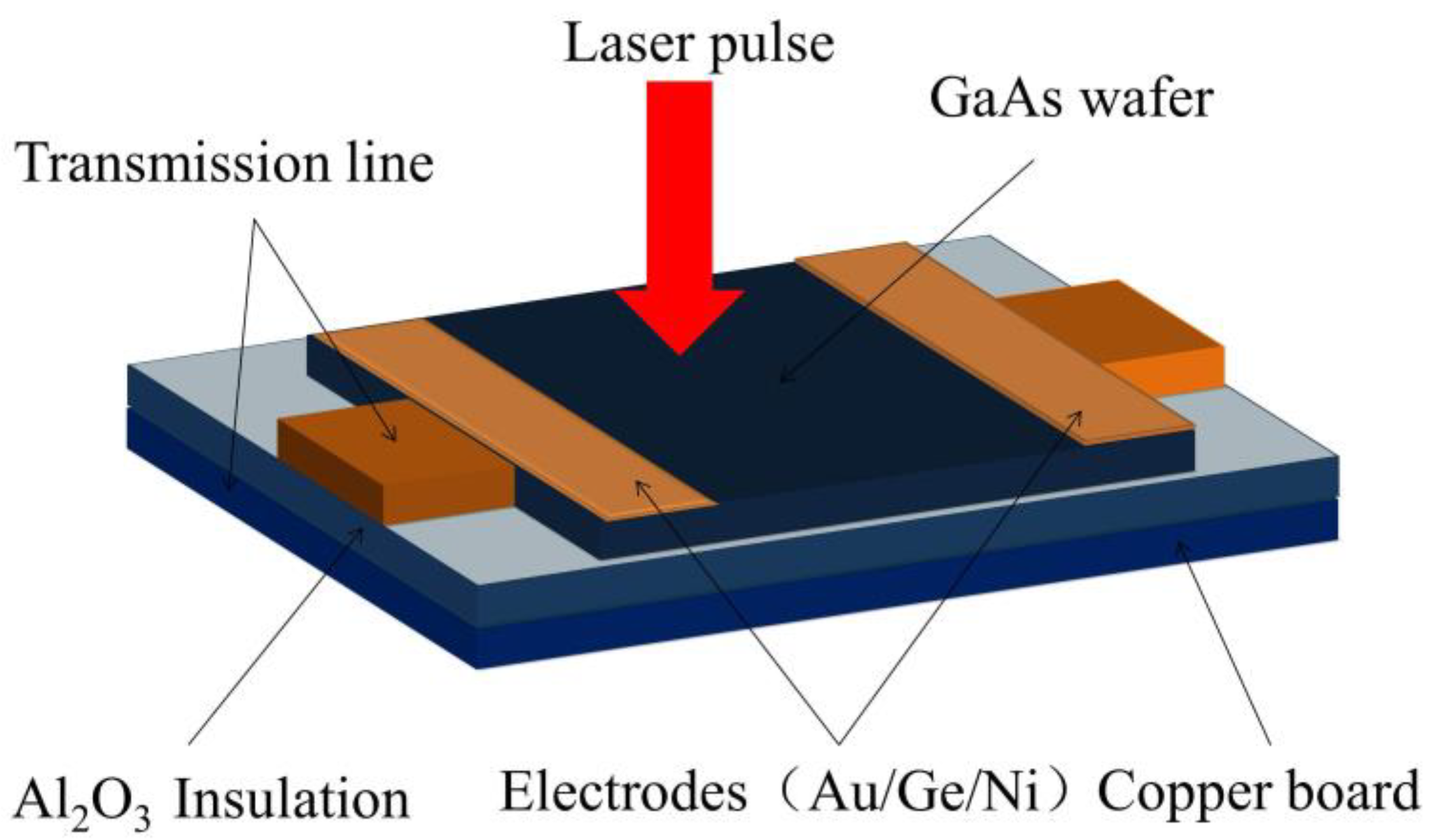
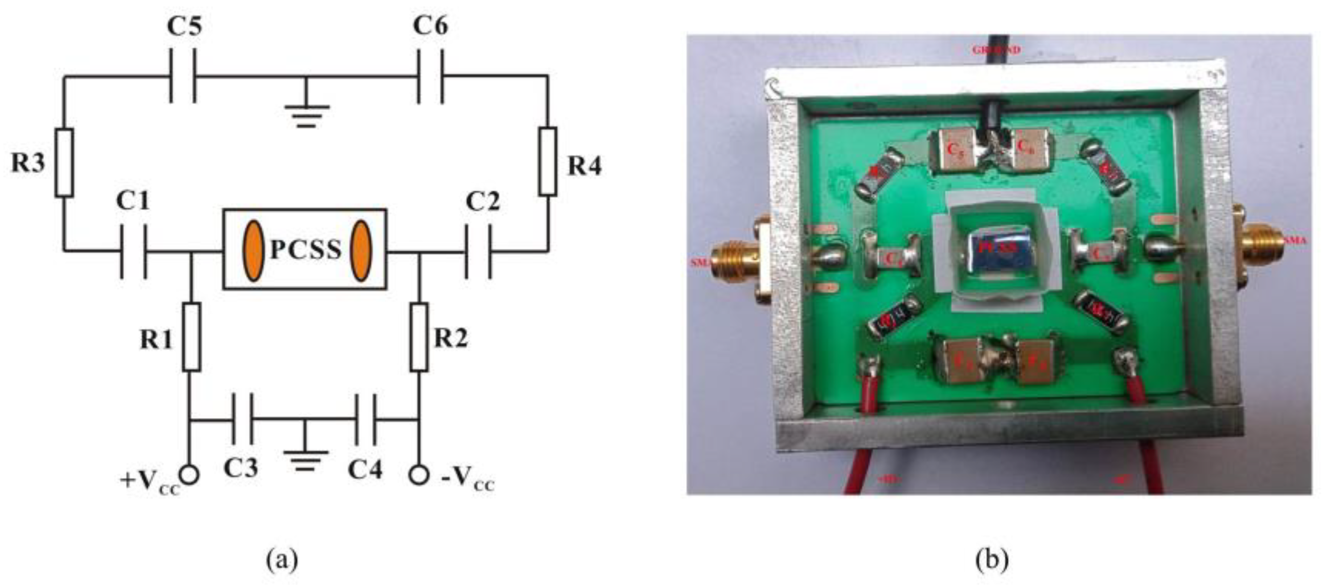
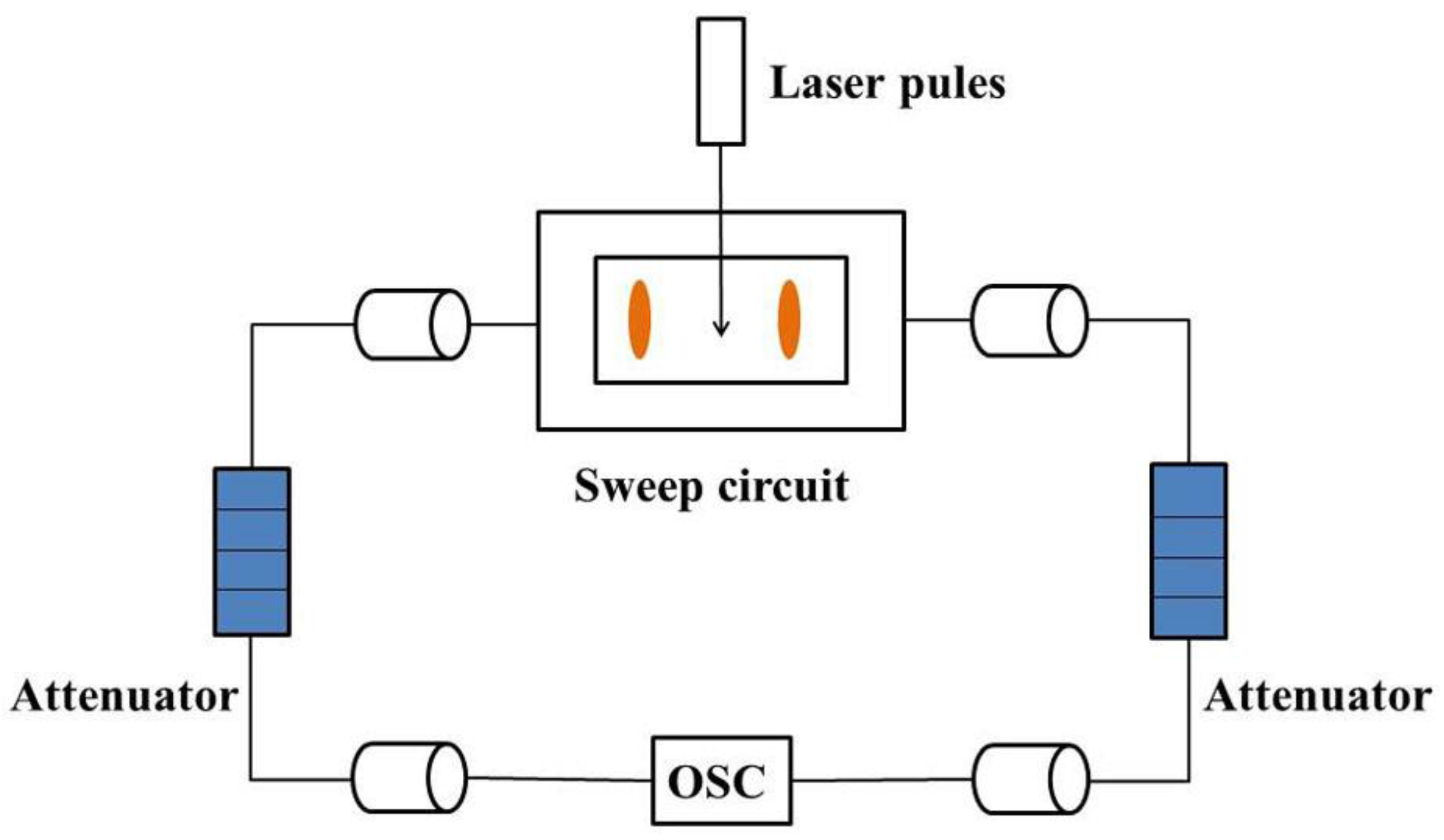
2. Experimental Setup

To meet the requirement of a femtosecond streak camera, a sweep circuit was designed, with the core component of GaAs PCSSs. The schematic diagram of a lateral GaAs PCSS for the experiment is shown in Figure 1. The bottom copper board is part of the transmission line, and the Al2O3 insulation layer is located between the copper board and GaAs substrate. The nominal dark resistance of the GaAs wafer is larger than 5 × 10⁷ Ω·cm, and the nominal electron mobility is higher than 5000 cm2/(V·s). The two Au/Ge/Ni electrodes form ohmic contact with the GaAs substrate. The size of each electrode is 6 mm × 3 mm, and the electrodes are rounded with the corner radius of 1.1 mm in order to uniform the electric field distribution. The gap between the two electrodes is 3.5 mm. Multi-layer transparent dielectrics used as the passivation and insulation protection materials are deposited and coated on the surface of the GaAs PCSS. The switch is connected with an external circuit using coaxial transmission lines.
The schematic diagram and the photo of bilateral sweep circuit based on the GaAs PCSSs are shown in Figure 2a,b, respectively. The capacitances of filter capacitors C1, C2, C5 and C6 are 10 nf. The capacitances of energy storage capacitors C3 and C4 are 33 pf. The resistances of current-limiting resistors R1, R2, R3 and R4 are 470 kΩ. In order to improve the circuit’s bandwidth, these capacitors and resistors are the surface-mounted components with small parasitic parameters and high voltage capacity (3000 V).
The experimental setup is shown in Figure 3. The sweep circuitwas connected with a 50 Ω coaxial line by sub-miniature-A (SMA) connectors. The output voltage was attenuated by 60-dB attenuators (BW-N20W50+ and BW-N40W50+, Mini circuits, NY, US) and recorded by an oscilloscope (OSC) (LeCroy WaveMaster 806Zi-A, 4x40GS/s, Teledyne LeCroy, NY, US) with a bandwidth of 6 GHz.

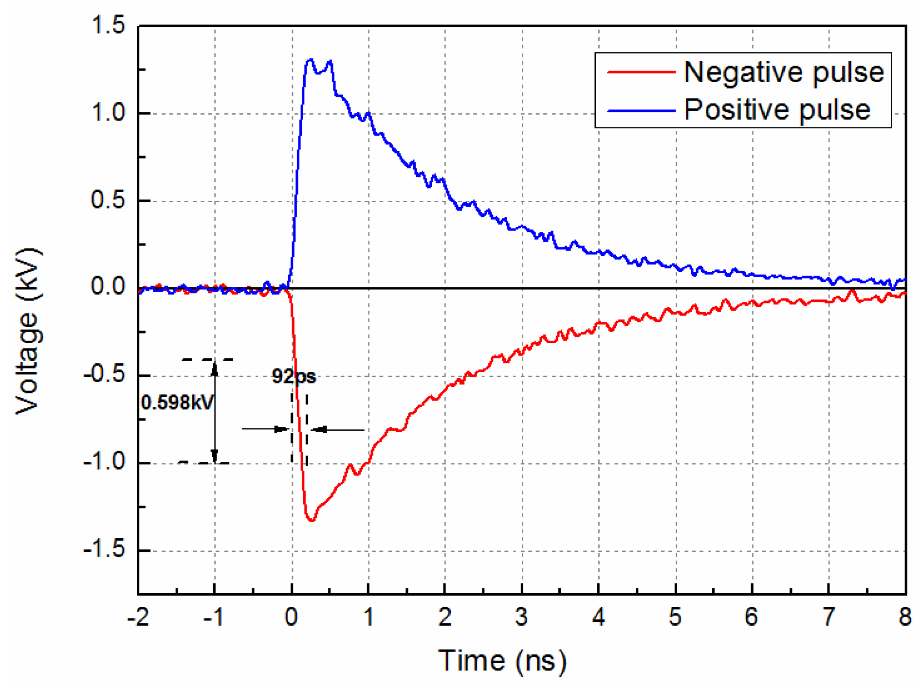
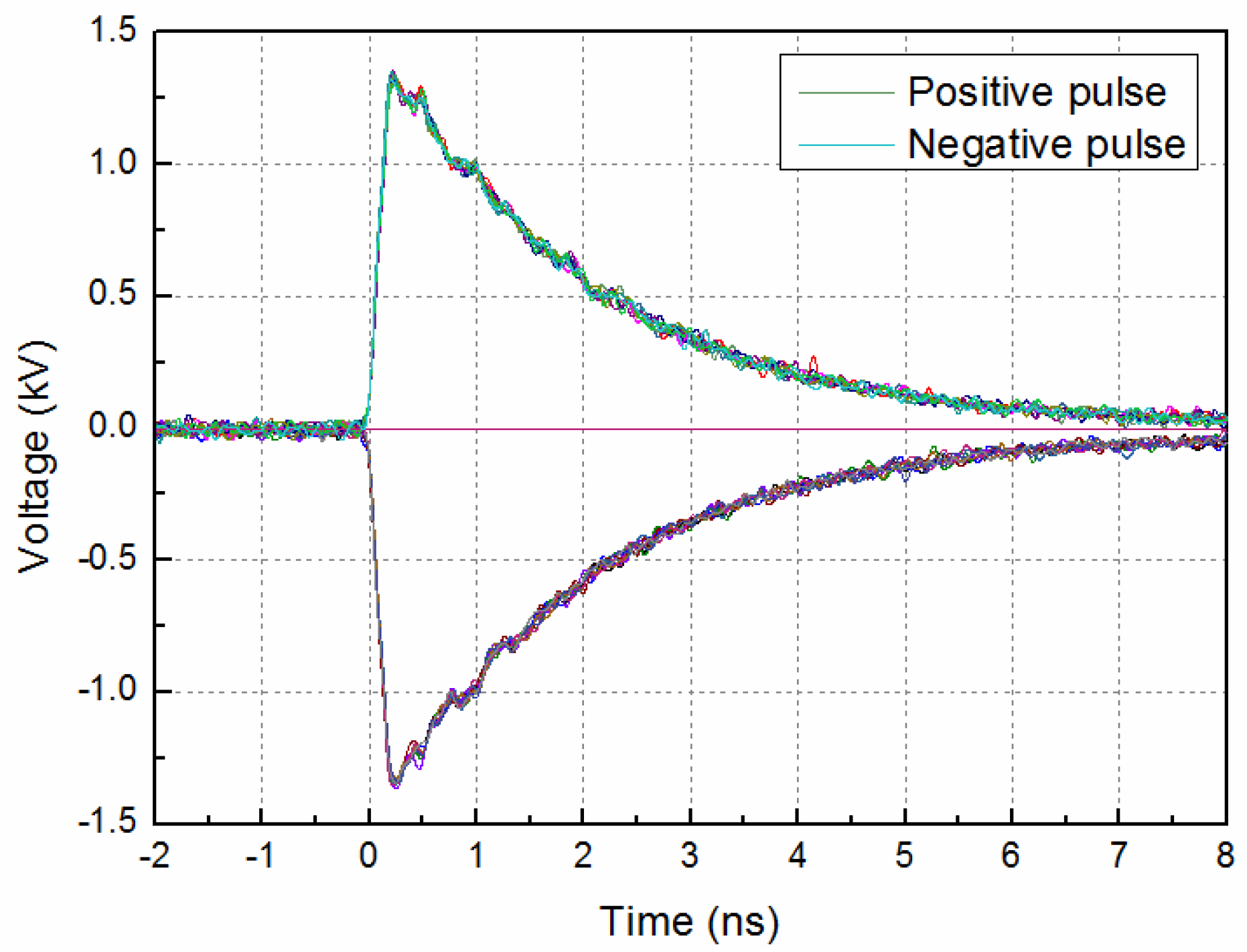
3. Results and Discussion

A regeneratively amplified mode-locked femtosecond Ti: sapphire laser with a pulse width of 100 fs and a wavelength of 800 nm was used as a trigger source, the laser pulse energy was 97.5 μJ, and the bias voltage was ±2.0 kV, according to the demand for the streak camera. The output waveform is shown in Figure 4.
As shown in Figure 4, the peak voltage of negative output pulse is 1.329 kV, and the transmission efficiency is 66.45%. The rise time of the pulse is 164 ps, and the time of linear range constitutes 92 ps with the corresponding voltage range of 0.598 kV, which yields a slope of 6.5 kV/ns. The rise time of positive pulse and the fall time of negative pulse are 174 ps and 164 ps, respectively, the difference is about 10 ps, and the error is about 6%, which is within the margin of error, for a femtosecond streak camera. The error is mainly caused by the electrical elements (resistors and capacitors) in electrical circuits, because their values are not exactly the same for two corresponding elements in the symmetric sweep circuits in Figure 2. The rise time of the pulse is mainly decided by the photoelectric response time of the GaAs substrate and the time duration of pump laser, and the pulse width is mainly decided by the lifetime of carriers of GaAs substrate. Moreover, the performance of the device can be improved by optimizing device geometry parameters. For example, the impedance of device elements should be matched by optimizing the microstrip line.
When the bias voltage is ± 2.0 kV, the electric field is 11.4 kV/cm. In our previous research [14], an avalanche gain (G) for high-gain operation was proposed to demonstrate the level of avalanche multiplication in the photoconduction process of a GaAs PCSS. The expression of G is shown in Equation (1):
G = N G / N L
where NG is the number of photo-activated carriers in high-gain operation and NL is the number of photons absorbed by SI–GaAs. However, the result shows that G is 1 × 10⁻³, that is, the carriers can not generate multiplication in this experiment.
When the GaAs PCSS operates in the linear mode, the jitter mainly comes from the instability of the laser performance [15,16,17]. In the previous research, the jitter time was 14.3 ps when GaAs PCSSs was triggered by the incident laser pulse with a time duration of 500 ps [1]. That is, the jitter time is much less when GaAs PCSS is triggered by a femtosecond laser pulse with a pulse duration of 100 fs. Now, the jitter time is so small that it cannot be measured by the 6 GHz oscilloscope. The 10 output waveforms measured at the same experiment condition are shown in Figure 5, and they overlap very well, which means the stability of our device is good. The relative standard deviation (RSD) of the output voltage can be defined as the stability of the PCSSs. Under each fixed bias voltage, one can obtain the stability of the PCSSs by calculating the RSD of the output voltage difference:
R S D = i = 1 n ( U i U ¯ ) 2 n 1 U ¯ × 100 %
where RSD is the stability of the PCSSs, U ¯ is the average of Ui, and n is the number of trigger times. In this way, the RSD values were measured as 1.3% and 0.83%, when the bias voltages were +2.0 and −2.0 kV, respectively, which is within the error range.

4. Conclusions

In this paper, the positive and negative symmetric pulses with a fast rising edge were obtained by using a GaAs PCSS and a sweep circuit. When the GaAs PCSS biased at 2.0 kV was triggered by a femtosecond laser pulse with the energy of 97.5 μJ and the time duration of 100 fs, the peak voltage of positive and negative pulses were 1.313 kV and 1.329 kV, respectively, and the rise times were 174 ps and 164 ps, respectively. Moreover, the RSD values of the output voltage of the GaAs PCSS were measured as 1.3% and 0.83% for the bias voltages of +2.0 and −2.0 kV, respectively, and the device presents good stability at 2.0 kV. The experimental results indicate that the GaAs PCSS can meet the requirements of a femtosecond streak camera.

Author Contributions

All the authors contributed to this study. W.S.: conceptualization, funding acquisition, project administration, supervision, writing of review and editing; L.Y.: investigation, writing of the original draft; L.H., Z.L., N.X. and Z.X.: investigation.

Funding

This study was supported in part by the National Natural Science Foundation of China under grant numbers 61427814 and 61575161, in part by the National Key Research and Development Program of China under grant number 2017YFA0701005, in part by the State Key Laboratory of Intense Pulsed Radiation Simulation and Effect of China under grant number SKLIPR1812.

Conflicts of Interest

The authors declare no conflicts of interest.

References

  1. Shi, W.; Zhang, L.; Gui, H.; Hou, L.; Xu, M.; Qu, G. Accurate measurement of the jitter time of GaAs photoconductive semiconductor switches triggered by a one-to-two optical fiber. Appl. Phys. Lett. 2013, 102, 154106. [Google Scholar] [CrossRef]
  2. Chao, J.; Zhu, W.; Chen, C.; Lee, Y.; Shang, A.; Yin, S.; Hoffman, R. Ruby fluorescence-enabled ultralong lock-on time high-gain gallium arsenic photoconductive semiconductor switch. Opt. Lett. 2018, 43, 3929–3932. [Google Scholar] [CrossRef] [PubMed]
  3. El Amari, S.; De Angelis, A.; Arnaud-Cormos, D.; Couderc, V.; Leveque, P. Characterization of a Linear Photoconductive Switch Used in Nanosecond Pulsed Electric Field Generator. IEEE Photonic Technol. Lett. 2011, 23, 673–675. [Google Scholar] [CrossRef]
  4. Shi, W.; Jiang, H.; Li, M.; Ma, C.; Gui, H.; Wang, L.; Xue, P.; Fu, Z.; Cao, J. Investigation of electric field threshold of GaAs photoconductive semiconductor switch triggered by 1.6 μJ laser diode. Appl. Phys. Lett. 2014, 104, 042108. [Google Scholar] [CrossRef]
  5. Hu, L.; Su, J.; Qiu, R.; Fang, X. Ultra-Wideband Microwave Generation Using a Low-Energy-Triggered Bulk Gallium Arsenide Avalanche Semiconductor Switch with Ultrafast Switching. IEEE Trans. Electron Devices 2018, 65, 1308–1313. [Google Scholar] [CrossRef]
  6. Vergne, B.; Couderc, V.; Barthélémy, A.; Gontier, D.; Lalande, M.; Bertrand, V. High-Voltage Rectifier Diodes Used as Photoconductive Device for Microwave Pulse Generation. IEEE Trans. Plasma Sci. 2006, 34, 1806–1813. [Google Scholar] [CrossRef]
  7. Itatani, J.; Quéré, F.; Yudin, G.L.; Ivanov, M.Y.; Krausz, F.; Corkum, P.B. Attosecond streak camera. Phys. Rev. Lett. 2002, 88, 173903. [Google Scholar] [CrossRef] [PubMed]
  8. Auston, D.H. Picosecond optoelectronic switching and gating in silicon. Appl. Phys. Lett. 1975, 26, 101–103. [Google Scholar] [CrossRef]
  9. Smith, P.R.; Auston, D.H.; Nuss, M.C. Subpicosecond photoconducting dipole antennas. IEEE J. Quantum Electron. 1988, 24, 255–260. [Google Scholar] [CrossRef]
  10. Schmuttenmaer, C.A. Exploring Dynamics in the Far-Infrared with Terahertz Spectroscopy. Chem. Rev. 2004, 104, 1759–1779. [Google Scholar] [CrossRef] [PubMed]
  11. Liu, J.; Wang, J.; Shan, B.; Wang, C.; Chang, Z. An accumulative x-ray streak camera with sub-600-fs temporal resolution and 50-fs timing jitter. Appl. Phys. Lett. 2003, 82, 3553–3555. [Google Scholar] [CrossRef]
  12. Maksimchuk, A.; Kim, M.; Workman, J.; Korn, G.; Squier, J.; Du, D.; Umstadter, D.; Mourou, G.; Bouvier, M. Signal averaging x-ray streak camera with picosecond jitter. Rev. Sci. Instrum. 1996, 67, 697–699. [Google Scholar] [CrossRef] [Green Version]
  13. Ji, W.; Shi, W.; Jia, W. Ultrafast rising of output electric impulse of high gain semi-insulated GaAs PCSS. In Proceedings of the 2011 International Conference on Electronics and Optoelectronics, Dalian, China, 29–31 July 2011; pp. V3284–V3286. [Google Scholar]
  14. Xu, M.; Li, R.; Ma, C.; Shi, W. 1.23-ns Pulse width of Quenched High Gain GaAs Photoconductive Semiconductor Switch at 8-nJ Excitation. IEEE Electron Device Lett. 2016, 37, 1147–1149. [Google Scholar] [CrossRef]
  15. Shi, W.; Gui, H.; Zhang, L.; Ma, C.; Li, M.; Xu, M.; Wang, L. Effects of trigger laser pulse width on the jitter time of GaAs photoconductive semiconductor switch. Opt. Lett. 2013, 38, 2330–2332. [Google Scholar] [CrossRef] [PubMed]
  16. Gui, H.; Shi, W.; Ma, C.; Fan, L.; Zhang, L.; Zhang, S.; Xu, Y. The jitter time of GaAs photoconductive switch triggered by 532- and 1064-nm laser pulse. IEEE Photonics Technol. Lett. 2015, 27, 2001–2003. [Google Scholar] [CrossRef]
  17. Shi, W.; Gui, H.; Zhang, L.; Li, M.; Ma, C.; Wang, L.; Jiang, H. Influence of the incident laser pulse energy on jitter time of GaAs photoconductive semiconductor switches. Opt. Lett. 2013, 38, 4339–4341. [Google Scholar] [CrossRef] [PubMed]
Figure 1. Schematic diagram of a lateral PCSS.
Applsci 09 00358 g001
Figure 2. (a) Schematic diagram of the sweep circuit; (b) The photo of the sweep circuit.
Applsci 09 00358 g002
Figure 3. Schematic diagram of the testing circuit.
Applsci 09 00358 g003
Figure 4. The output waveform at a bias voltage of ± 2.0 kV and a laser pulse energy of 97.5 μJ.
Applsci 09 00358 g004
Figure 5. The output waveforms at a bias voltage of ± 2.0 kV and a laser pulse energy of 97.5 μJ.
Applsci 09 00358 g005

