1. Introduction
In the last decades, the possibility to structure the spatial degree of freedom of light has acquired increasing interest, with applications in a wide range of fields. In particular, the exploitation of light beams with helical phase-fronts has provided disruptive achievements in microscopy [
1,
2], astronomy [
3], particle manipulation [
4], holography [
5], and information and communication technology (ICT) [
6,
7]. Since the seminal paper of Allen and coworkers [
8] demonstrated that such beams carry orbital angular momentum (OAM), the study on methods and devices to generate and control this still unexploited degree of freedom has given rise to a flourishing research field [
9]. It is especially in the ICT that the orbital angular momentum of light has demonstrated the most promising applications, in combination with other degrees of freedom of light [
10]. As a matter of fact, the OAM degree of freedom opens to an unbounded state space, in which light beams carrying different integer OAM values are orthogonal to each other and can be exploited for the transmission of different data streams at the same frequency with no interference [
11]. The aggregate combination of OAM-mode division multiplexing (OAM-MDM) with other well-established multiplexing methods, e.g., time, polarization, wavelength, and amplitude/phase, has demonstrated to provide a significant increase in the spectral efficiency of today’s optical networks [
12], both in free-space [
13] and optical fibers [
14,
15], offering a solution to the problem of optical network saturation [
16]. Both in the classical and quantum regimes, the combined manipulation of OAM and polarization has acquired paramount importance, and novel devices are required for the parallel detection in a compact and effective way. As a matter of fact, optical vortices propagating in multi-mode fibers have been demonstrated to be circularly polarized [
15]. In the single-photon regime, the combination of orbital angular momentum and polarization opens to a wider state space for quantum-key distribution (QKD) applications [
17], in which higher security and robustness against errors and eavesdropping are guaranteed with respect to standard protocols limited to polarization [
7]. Novel formulations and innovative implementations of standard QKD protocols have been developed and demonstrated [
18], both in discrete variable (DV-QKD) and continuous variable (CV-QKD) scenarios [
19]. Concurrently, research efforts have focused on the design and realization of polarization-sensitive OAM (de)multiplexers, in order to generate and sort the state space exploited for high-dimensional QKD [
20,
21].
In the last decade, several methods have been conceived for demultiplexing, i.e., the separation, of a superposition of beams with different values of OAM [
22]. In particular, increasing interest has been devoted to solutions which could offer high miniaturization and integration levels, fabrication protocols suitable for mass-production, and backward compatibility with different multiplexing techniques. In order to improve the miniaturization level, we recently disclosed the realization of 3D multi-level phase-only diffractive optical elements [
23,
24,
25,
26] performing OAM-mode generation and detection in the visible range, based either on
log-pol optical transformation [
27] or OAM-mode projection [
28,
29]. In comparison with bulky refractive elements, the diffractive version provides a miniaturized and almost flat implementation, in particular, when shorter focal lengths are necessary, i.e., for high miniaturization. On the other hand, the design of diffractive optics turns out to be optimized within a narrow bandwidth, therefore they exhibit a decrease in efficiency when operating far from the optimal wavelength. The optical thickness is inversely proportional to the refractive index of the material, and increases proportionally to the design wavelength. If the transparency of silicon in the telecom infrared suggests the exploitation of this high-refractive index material in order to further reduce the optical thickness, then, on the other hand, the fabrication of 3D surface-relief patterns in silicon is still undoubtedly challenging.
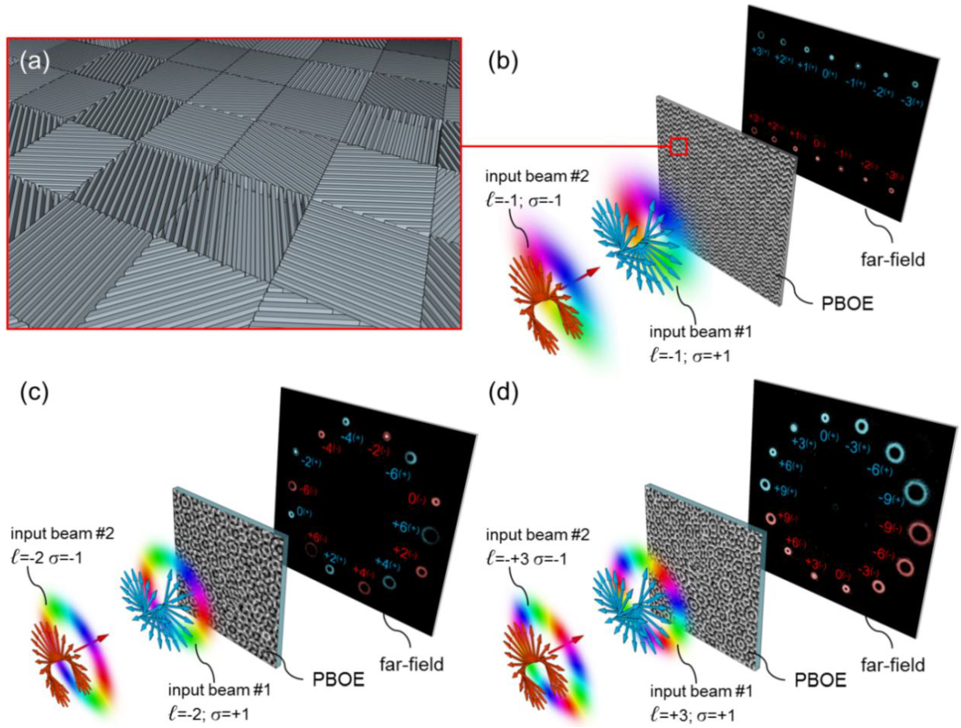
An alternative method for phase-fronts manipulation is provided by Pancharatnam–Berry optical elements (PBOE) acting on the geometric phase of light. Unlike refractive and diffractive optics, in PBOEs the phase change is not produced by means of an optical path difference, but is the result of a space-variant modification of the polarization state of light [
30]. This is achieved by realizing an artificial material, i.e., a metasurface, which is both inhomogeneous and anisotropic, in order to create an effective anisotropic medium whose extraordinary axis orientation is spatially variant. The phase transferred to the input beam is equal to twice the value of the fast-axis orientation, therefore by properly engineering the anisotropy pattern it is possible to reshape the input phase-front in the desired way. With respect to conventional optics, the approach with metasurfaces can offer greater advantages owing to their digital profile and fixed thickness. In comparison with diffractive optics, metasurfaces show a broader band [
31], since the wave-front is tailored by the geometric pattern of the optical element. In addition, since the optical response becomes inherently dependent on the input polarization [
32], polarization-division multiplexing (PDM) can be easily implemented without the need of additional optics [
33].
In this paper, we present the design and realization of sorting optics for OAM-MDM, in the form of Pancharatnam–Berry optical elements in silicon for the telecom wavelength of 1310 nm. We considered the demultiplexing method based on OAM-mode projection and we computed and realized different metasurfaces in silicon, performing both OAM-MDM and PDM. Despite its lower efficiency with respect to other methods, this technique allows to customize the channel constellation and the sorting OAM range, depending on the desired application. Different OAM sets and far-field channel configurations have been selected and presented, in order to demonstrate the versatility offered by this demultiplexing method.
The birefringence of the single PBOE subunit has been achieved artificially by structuring the silicon substrate with a digital subwavelength grating, which is experienced by the impinging wave as a uniaxial crystal whose fast axis is perpendicular to the grating ridges [
34]. The resist mask fabricated on the silicon surface with high-resolution electron-beam lithography (EBL) was transferred to the substrate by a finely-tuned inductively coupled plasma—reactive plasma etching (ICP-RIE) process. The optical tests at the wavelength of 1310 nm, in the telecom O-band, confirm the expected capability of the designed optics to detect correctly input beams with different circular-polarization states and orbital angular momentum values.
2. Materials and Methods
2.1. Phase Pattern Calculation
A diffractive optical element designed to analyze the OAM spectrum in the set of OAM values {
ℓj} presents a phase pattern Ω(
u,
v) which is given by the linear superposition of
n orthogonal OAM modes {
ψj} as follows [
35]:
being {
ψj =
Rj(
ρ,
ϑ)exp(
iℓjϑ)}, where
ϑ = arctan(
v/
u),
, {
Rj(
ρ,
ϑ)} describe the field spatial distributions and depend on the family of modes. {(
αj,
βj)} are the
n vectors of carriers spatial frequencies in Cartesian coordinates, and {
cj} are complex coefficients whose modulus is usually unitary, and the phases are fitted so that Equation (1) is an exact equality [
23]. The set of parameters {
cj} is calculated with the following integral:
The diffractive element is basically a computer-generated hologram originated from the linear combination of
n fork-holograms. Each term in Equation (1) is given by the interference pattern of the
jth OAM-mode with azimuthal phase term exp(
iℓjϑ) with the tilted plane-wave exp(
iαju + iβjv) defined by the corresponding carrier frequency. In the Fourier plane, the carrier frequencies manifest as separate spatial coordinates {(
xj,
yj)} given by:
being
f the focal length of the lens which is used for far-field reconstruction in
f-
f configuration, and
k = 2π/
λ, where
λ is the working wavelength. When the optical element is illuminated with an integer OAM beam, the projection of the beam is optically performed over the selected OAM set, and a bright spot appears at the position corresponding to the input OAM value in far field (
Figure 1) [
23].
In a metasurface realization of the optical element, the phase pattern Ω(
u,
v) is obtained by fabricating an inhomogeneous and anisotropic effective medium, whose extraordinary-axis orientation
θ(
u,
v) changes point-by-point and is equal to half the local phase value Ω(
u,
v). The two orthogonal circular polarizations exhibit a different behavior, as it follows [
32]:
being
T the transmission matrix of the optical element,
δ the phase delay between the ordinary and extraordinary axes of the metasurface effective medium, [1, +
i] and [1, −
i] the vectors of right-handed and left-handed circular polarizations in Jones matrix formalism, respectively (the normalization factor
has been omitted). In particular, when the metasurface is engineered in order to achieve the condition
δ = π (π-delay between the two optical axes), the zero-order term is cancelled out and a total polarization conversion is obtained:
In this case, the two orthogonal circular polarizations experience opposite phase patterns:
and their corresponding sets of intensity spots appear at symmetric coordinates in far field:
where the subscripts (+) and (−) stand for right-handed and left-handed circular polarizations, respectively.
As expressed by Equation (7), a beam carrying OAM equal to ℓ and right-handed circular polarization generates a bright spot at a position which is center-symmetric to the spot formed by the left-handed circularly-polarized state with opposite value of OAM. Hence, during the design of a metasurface performing demultiplexing over a properly-designed set of modes, particular attention should be paid to carefully choosing the spatial frequency carriers in order to prevent different channels from overlapping.
A custom code has been developed in MATLAB
® in order to compute the phase patterns for the selected set {
ℓj} of OAM values and the corresponding carriers frequencies {(
αj,
βj)}. The implemented algorithm is based on a successive computation of the integrals in Equation (2) and of the sum in Equation (1), implementing the fast Fourier transform algorithm and applying precise constrains, as explained in [
5,
23], in particular phase quantization into 16 equally-spaced values in the range [0, 2π).
In the following, three different configurations are presented and described. Each phase pattern performs the demultiplexing of circularly-polarized beams over 7 OAM values, for a total of 14 channels, with different OAM separation and far-field channel constellation: Linear array, regular polygon, semicircle.
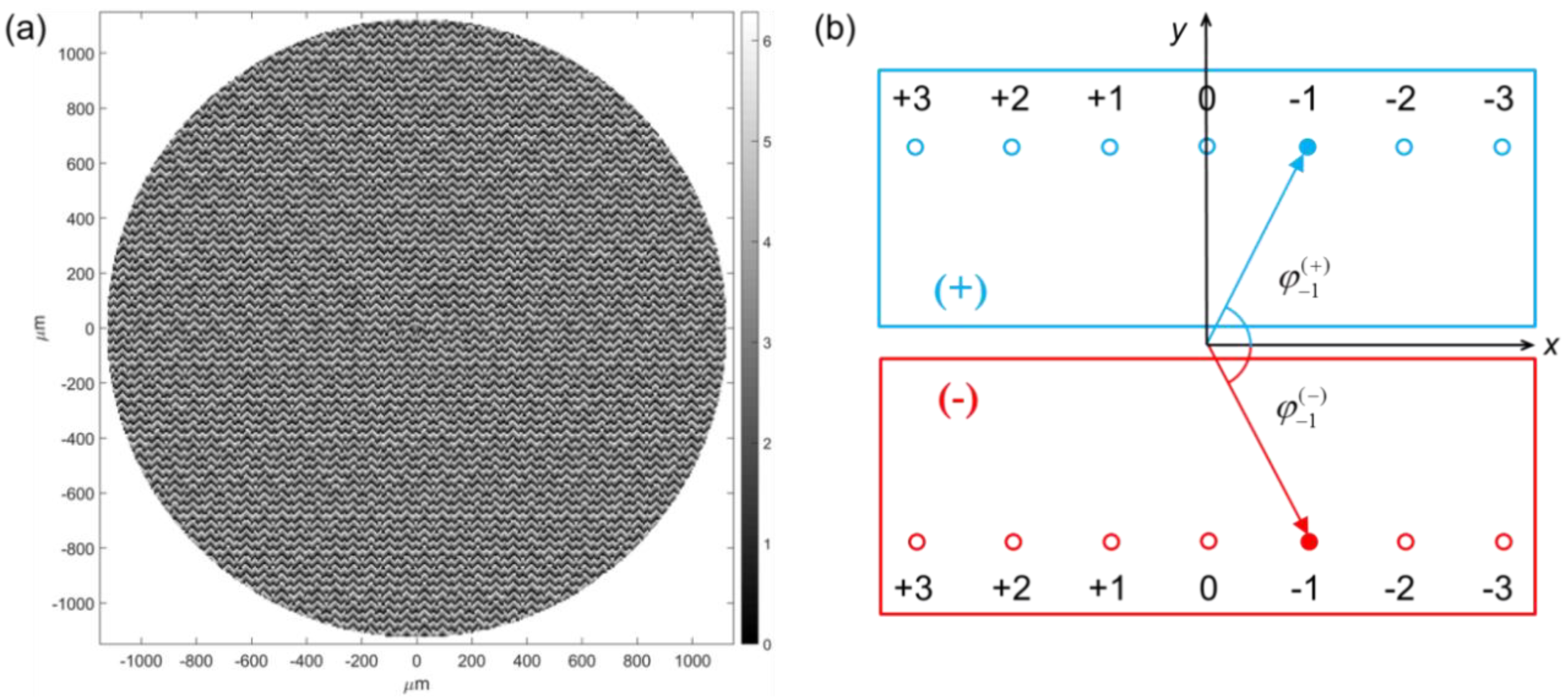
2.1.1. Linear Array
We limited the choice to OAM values in the set from
ℓ = −3 to
ℓ = +3 for a total of 7 OAM values (
n = 7). The spatial frequencies have been fixed in such a way that the far-field peaks were arranged along a line at equally spaced
x-positions (see
Figure 2b):
where
j = 1, …7. Considering Equation (7) and the symmetry of the far-field channels constellation, it results that:
The two orthogonal polarizations are therefore sorted over two distinct linear arrays without overlapping, as depicted in
Figure 2b.
2.1.2. Regular Polygonal Configuration
We considered the OAM values in the set {−6, −4, −2, 0, +2, +4, +6} for a total of 7 OAM channels. We fixed the carrier spatial frequencies in order to arrange the far-field peaks at the vertices of a regular polygon, in the specific case a heptagon. In polar coordinates, the spatial frequencies are given by {(
ρj,
θj)} = {(
γ,
j2π
/7)},
j = 1, …7. Therefore, the far-field points appear at equally-spaced angular positions, specified as follows:
where
j = 1, …7, being
r the radius of the circumscribed circle. According to Equation (7), we have:
that is
The two orthogonal polarizations are sorted over two overlapping heptagons, as shown in the scheme in
Figure 3b. According to Equation (12), the far-field intensity peaks are expected to be at the following angular positions for the left-handed beams:
As shown in
Figure 3b, for increasing OAM values, the corresponding spots appear counterclockwise (clockwise) for incident right-handed (left-handed) circular polarization.
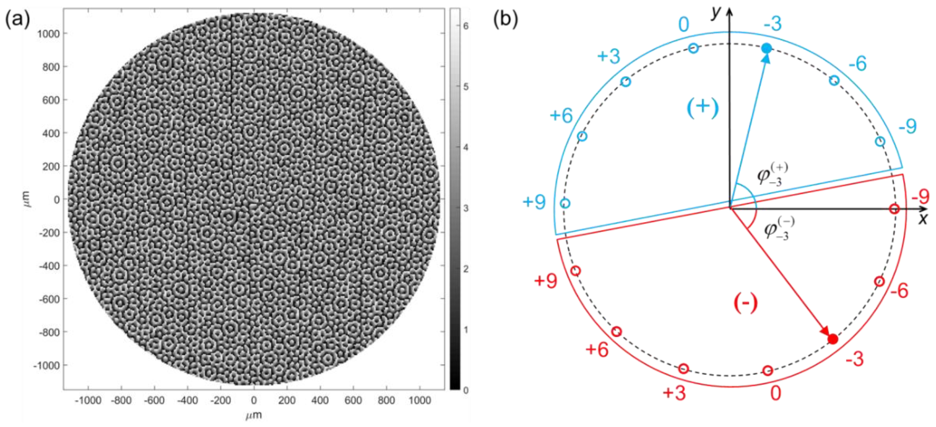
2.1.3. Equally-Spaced Hemi-Circular Configuration
In order to arrange the far-field channel at equally-spaced angular positions without overlap, a semicircle configuration appears to be the best choice. In this case we considered the set {−9, −6, −3, 0, +3, +6, +9} and we fixed the carrier spatial frequencies in such a way that the far-field peaks were arranged over a semicircle of constant radius
r at equally-spaced angular positions (see
Figure 4b), specified as follows:
where
j = 1, …7. According to Equation (7), the far-field intensity peaks are expected to be at the following angular positions:
The two orthogonal polarizations are therefore sorted over two complementary semicircles without overlapping, as shown in the scheme in
Figure 4b.
2.2. Subwavelength Grating Design
The metasurface version of the computed optical elements has been realized in the form of spatially-variant subwavelength gratings, whose ridges orientation is rotated pixel-by-pixel introducing a spatially-dependent form birefringence. The key element of the metasurface is represented by the subwavelength linear grating cell, whose local orientation
θ(
u,
v) is fixed in order to transfer the desired geometric-phase Ω(
u,
v) to the input wavefront, according to Reference [
36]:
being (
u,
v) the coordinates of the reference frame on the optical element plane. The phase-patterns of the designed optical elements have been calculated as 4-bit grayscale images (16 phase levels) and converted into subwavelength grating metasurfaces with custom MATLAB
® codes. The gray level
j, in the range from 0 to 15, has been associated to the rotation angle
j2π/32 of the corresponding subwavelength grating vector. For a given grating thickness, numerical simulations must be performed in order to identify the optimal profile, in terms of duty-cycle and period, providing the maximum conversion efficiency, i.e., π-delay between ordinary and extraordinary axes. In Reference [
36], a numerical study was performed implementing Rigorous Coupled-Wave Analysis (RCWA) [
37,
38] for a binary silicon grating in air at 1310 nm, in order to extract the optimal configurations of period and duty-cycle which provide π-retardation. For a thickness of 535 nm with a duty-cycle around 0.5, the grating period providing a π-delay is around 290 nm. This configuration was chosen for the design and fabrication of the silicon PBOEs presented in this study.
2.3. Fabrication
For the fabrication of subwavelength gratings with high aspect ratio a three-step stamp process was considered. Electron-beam lithography (EBL) provides the ideal method to transfer the computational patterns from a digitally-stored format to a physical layer with high-resolution profiles. The original EBL pattern was transformed into an imprinting mold for subsequent imprinting replica and inductively coupled plasma—reactive ion etching (ICP-RIE) to achieve the final sample.
Electron-beam lithography was performed with a JBX-6300FS EBL machine (JEOL, Tokyo, Japan) 12 MHz, 5 nm resolution, working at 100 kV with a current of 100 pA. A thin layer of positive resist (AR-P 672.03, ALLRESIST GmbH, Strausberg, Germany) was spun at 4000 rpm obtaining a thickness around 130 nm, followed by a hot plate soft-baking process at 150 °C for 3 min. Afterwards, the sample was developed in an isopropyl alcohol (IPA):deionized water 7:3 solution for 60 s, in order to remove the exposed areas.
To achieve the transfer from the EBL-patterned resist to the Silicon substrate, a 7-seconds stripping process in O2 plasma was performed, followed by a 72-seconds etching in fluorine-based plasma with STS MESC MULTIPLEX ICP (SemiStar Corp, Morgan Hill, CA, USA).
Next, a Thermal-NanoImprint Lithography (T-NIL) was performed with a Paul-Otto Weber hydraulic press with heating/cooling plates, for high-resolution replica [
39,
40]. The process was conducted using the previously-etched EBL master as cast after a silanization process with Trichloro(1H,1H,2H,2H-perfluorooctyl)silane PFOTS (Thermo Fisher (Kandel) GmbH, Karlsruhe, Germany) [
41,
42]. A layer of MR-I 7010E was deposited on a silicon wafer at 1750 rpm, achieving a thickness around 120 nm, followed by a 2-min soft bake at 140 °C. The sample was placed in contact with the master within a system of compliances in order to homogenize the temperature and pressure on the entire surface. The T-NIL process was performed at 100 °C for 10 min at 100-bar pressure. At the end of the imprinting step, a temperature decrease down to 35 °C occurred, maintaining the pressure fixed at 100 bar.
After a 13-second O
2 treatment to remove the residual layer, a 10-nm Cr hard mask was deposited by
e-gun evaporation and the transfer of the resist pattern was carried out by a lift-off process in a sonicated acetone bath for 180 s. Finally, an ICP-RIE etching was performed to remove the residual layer and hence obtain the required grating thickness. The etching time was finely adjusted to reach a final depth around 535 nm, as recommended by numerical simulations. In
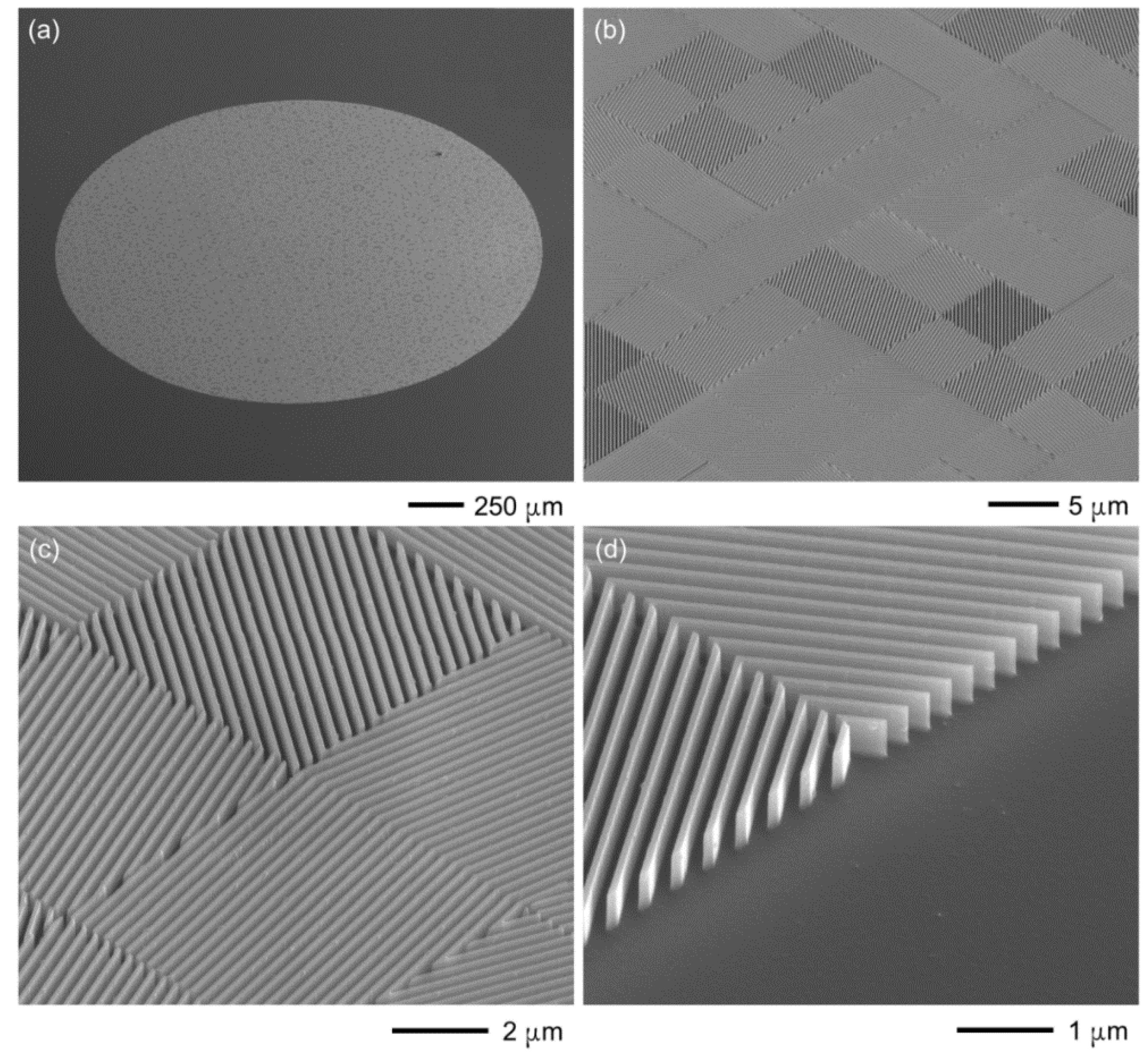
Figure 5, inspections at scanning electron microscopy (SEM) of the final sample are shown. In particular, the well-defined line profile is evidence of the suitability of the nanofabrication recipe for pattern transfer onto the silicon substrate.
2.4. Optical Characterization Setup
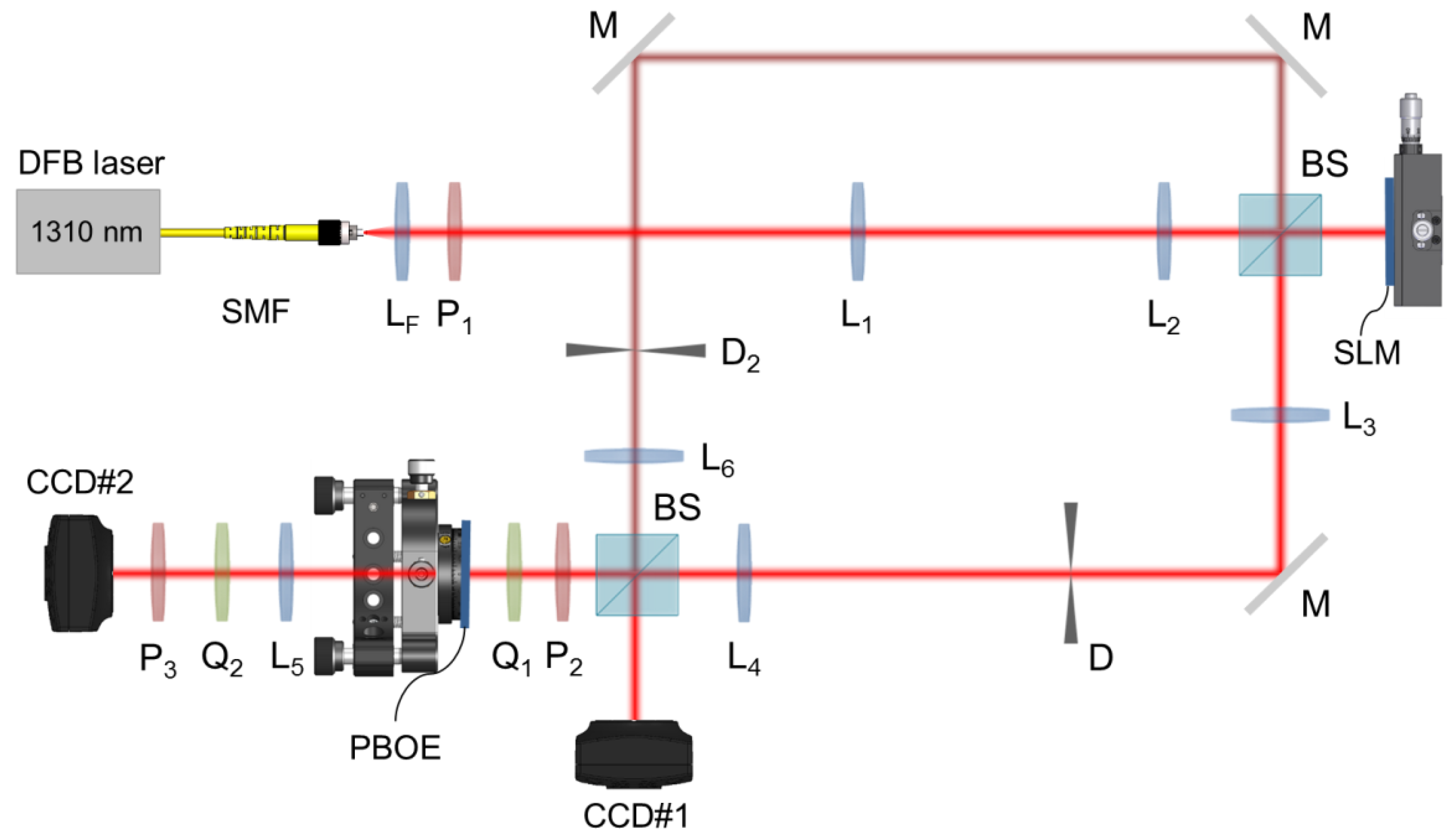
The experimental setup for the optical analysis of the fabricated samples is depicted in
Figure 6. The performance of the metasurfaces has been analyzed with input optical beams endowed with integer orbital angular momentum, generated by uploading the proper phase patterns on a LCoS spatial light modulator (SLM) (X13267-08, Hamamatsu, Shizuoka, Japan) with amplitude/phase modulation [
43]. An aspheric lens with focal length
fF = 7.5 mm (A375TM-C, Thorlabs, Newton, NJ, USA) was used to collimate the output of a DFB laser (
λ = 1310 nm) emerging at the end of a single mode fiber. Then the output beam was linearly polarized and expanded with a first telescope (
f1 = 3.5 cm,
f2 = 10.0 cm) before illuminating the display of the SLM. A beam-splitter (50:50) was inserted after the telescope in order to produce a second coherent Gaussian beam for interferometric analysis. A second telescope (
f3 = 20.0 cm,
f4 = 12.5 cm) with an aperture in the Fourier plane was used to isolate and image the first-order encoded mode onto the sorter. A second beam-splitter (50:50) was used to split the beam and check the input beam profile with a first camera (WiDy SWIR 640U-S, NIT, Verrières-le-Buisson, France). A Mach–Zehnder interferometric bench was added, as shown in
Figure 6, in order to analyze the phase pattern of the modes generated with the SLM. Afterwards, the OAM beam illuminated the silicon sample, mounted on a 6-axis kinematic mount with micrometer drives (K6XS, Thorlabs, Newton, NJ, USA). Finally, a second camera (WiDy SWIR 640U-S, NIT, Verrières-le-Buisson, France) was used to collect the far field at the back-focal plane of a lens with focal length
f5 = 7.5 cm. A sequence of linear polarizer (LPIREA100-C, Thorlabs, Newton, NJ, USA) and quarter-wave plate (WPQ10M-1310, Thorlabs, Newton, NJ, USA) was placed before and after the sorter, in reverse order, to control and select the circular polarization state of the input and output beams.
3. Results
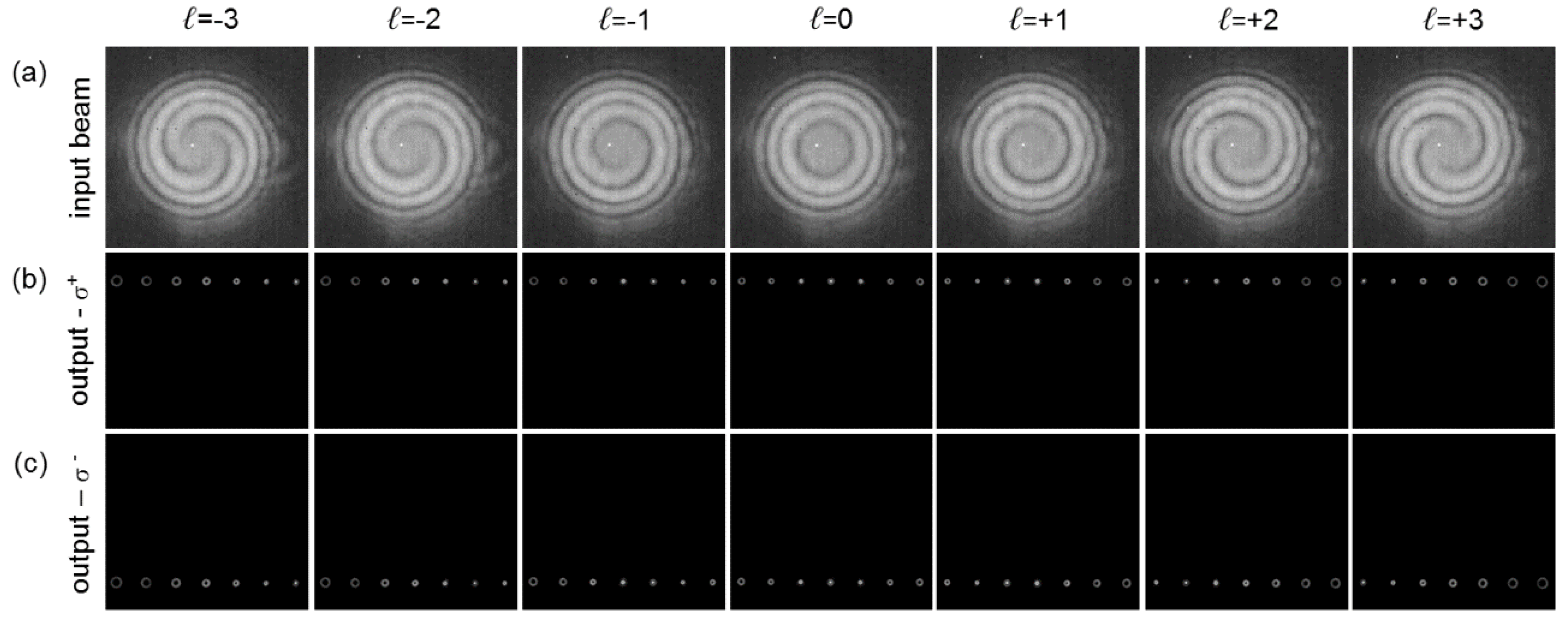
The output of the fabricated PBOEs has been analyzed and recorded for input circularly-polarized beams with well-defined OAM. For each PBOE, beams carrying OAM in the sorting set of the selected metasurface have been produced, in sequence, and circularly polarized before impinging on the optical element, according to the scheme in
Figure 6. Using a Mach–Zehnder interferometric bench, as shown in
Figure 6, the interference pattern between the generated OAM beam and a reference Gaussian beam was generated and collected in order to check the input OAM value. As a matter of fact, since the phase structure of an integer-OAM beam presents
ℓ intertwined helical phase fronts, being
ℓ the amount of OAM, the interference with a coaxial Gaussian beam generates a fringe pattern of
ℓ spirals, whose helicity is given by the sign of
ℓ [
44] (
Figure 7a,
Figure 8a, and
Figure 9a).
When a beam carrying OAM illuminates the demultiplexer, the optical element performs the projection over the mode set for which the phase pattern has been calculated. Next, a bright spot is detected in correspondence of the input OAM value, when it is present, at the coordinates given by corresponding far-field channel scheme. Otherwise, a non-null OAM beam is generated, i.e., an annular intensity profile with a central dark singularity.
In
Figure 7, the optical characterization is reported for the PBOE performing OAM sorting in the range {−3, …, +3} with OAM step Δ
ℓ = 1 (
Figure 7a). In
Figure 7b,c, the far field is shown for input beams with right-handed and left-handed circular polarizations, respectively. As expected, the demultiplexer can sort the orthogonal polarization states onto two different linear arrays, while the OAM value is detected correctly according to the scheme in
Figure 2b. A similar analysis is reported in
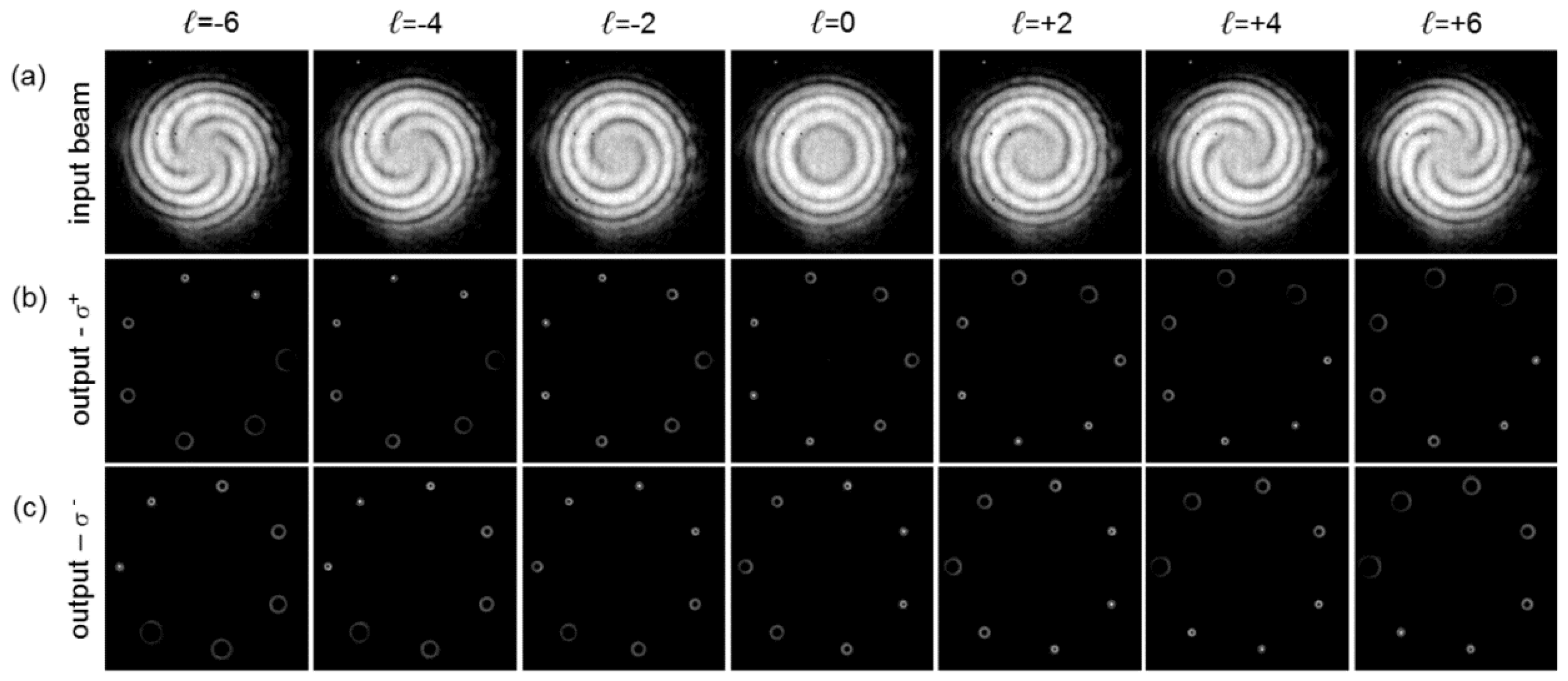
Figure 8, for the PBOE performing OAM demultiplexing in the range {−6, …, +6}, step Δ
ℓ = 2, according to the scheme in
Figure 3b. In
Figure 8b,c, the far field is shown for input optical vortices with right-handed and left-handed circular polarizations, respectively. The demultiplexer separates the orthogonal polarization states onto two heptagons, while the OAM content is detected correctly.
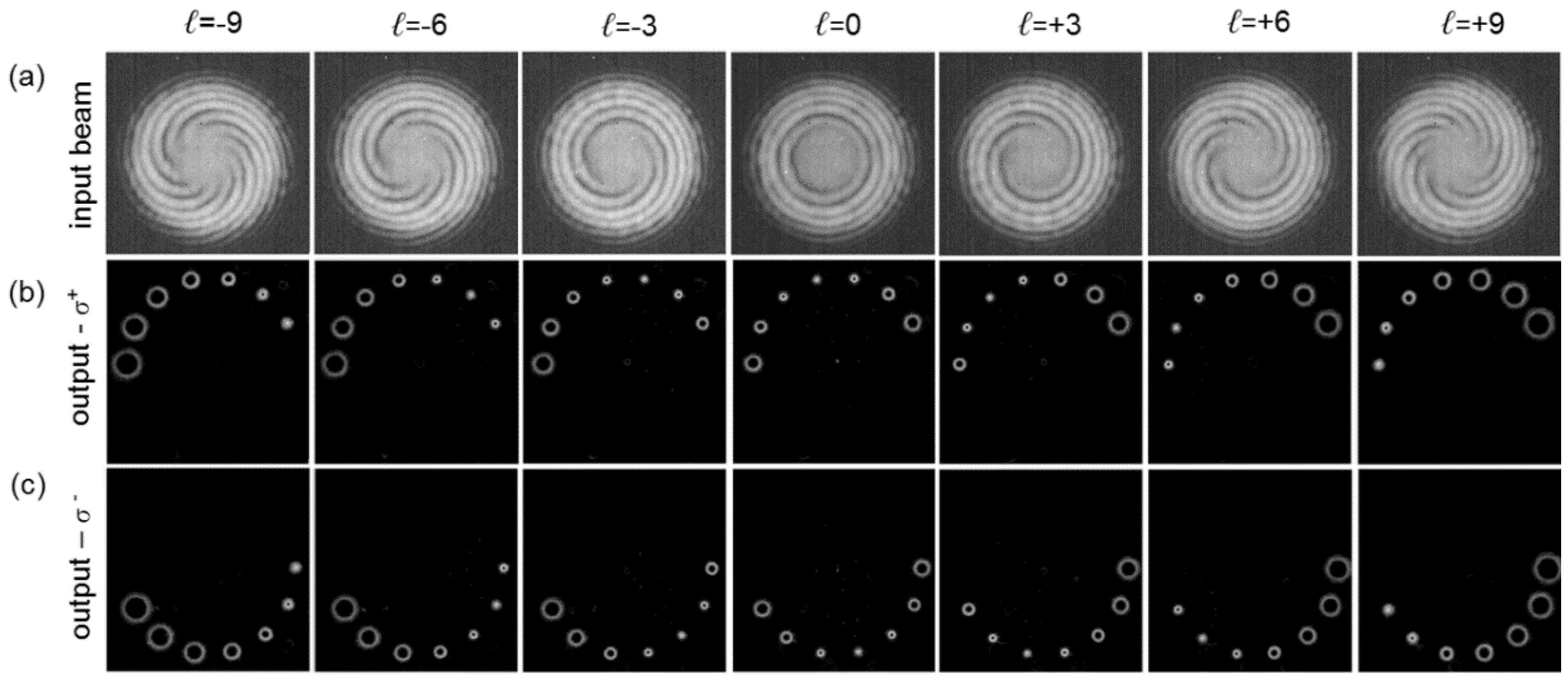
Figure 9 reports the optical analysis of the PBOE performing sorting in the OAM range {−9, …, +9}, step Δ
ℓ = 3, over a circular configuration, as depicted in the scheme in
Figure 4b. In
Figure 9b,c, the far field is shown for input vortices with right-handed and left-handed circular polarization, respectively. As expected, the demultiplexer can distinguish between orthogonal polarization states, by projecting them onto two complementary, i.e., non-overlapping, semicircles.
4. Discussion
In this work, we described the design, nanofabrication, and optical characterization of silicon metasurfaces for the parallel sorting of orbital angular momentum and polarization using the method of optical-mode projection. The samples were fabricated in the form of dielectric Pancharatnam–Berry optics, whose inhomogeneous anisotropy imparts a spatially-variant phase-change due to a local control of the input polarization. In particular, the phase is geometric in nature and equal to twice the rotation angle of the local extraordinary axis, corresponding to the direction of the subwavelength grating vector. Three different sorters have been designed and fabricated, performing combined PDM and OAM-MDM over different OAM sets and channel configurations, with the aim to exhibit the versatility of the demultiplexing method in terms of channels geometry and OAM values. In particular, we demonstrated the possibility to sort a symmetric range of OAM beams over a linear array and over 2D regular distributions, specifically a regular polygon and a semicircle. By properly designing the far-field channel scheme, fixed by the spatial frequency carriers in the phase pattern definition of the sorter, it was possible to originate two non-overlapping channel geometries for the two orthogonal polarizations. The optical characterization has been reported at the wavelength of 1310 nm, in the telecom O-band, showing the expected capability to distinguish between modes with different orbital angular momentum and spin values by using a single element. With respect to the diffractive counterpart [
23], the number of available channels is redoubled without the need of additional optical elements.
Metasurfaces have become one of the most rapidly expanding frontiers of nanophotonics to revolutionize optics by substituting refractive and diffractive optics in many widespread applications and introducing entirely altogether novel functionalities [
45,
46]. In particular, the possibility to use silicon as optical material has promoted the flourishing of a new framework in which optics design and silicon photonics merge to create a new generation of optical elements with unprecedented levels of integration. In comparison with plasmonic metamaterials, the importance of silicon in optics design and fabrication is based not only on its optical properties, low-cost, and well-established nanofabrication techniques, but also on the peculiar and promising prospects that silicon nanostructures can provide in terms of integration into existing photonic architectures and complementary metal-oxide semiconductor (CMOS) compatibility [
47,
48].
By including optics design and silicon photonics, the presented metasurfaces pave the way to novel optical devices for combined polarization- and OAM-mode division multiplexing with an unprecedented combination of miniaturization and integration.


