
Compact SOI Dual-Mode (De)multiplexer Based on the Level Set Method

Abstract
:1. Introduction
2. Design Principle
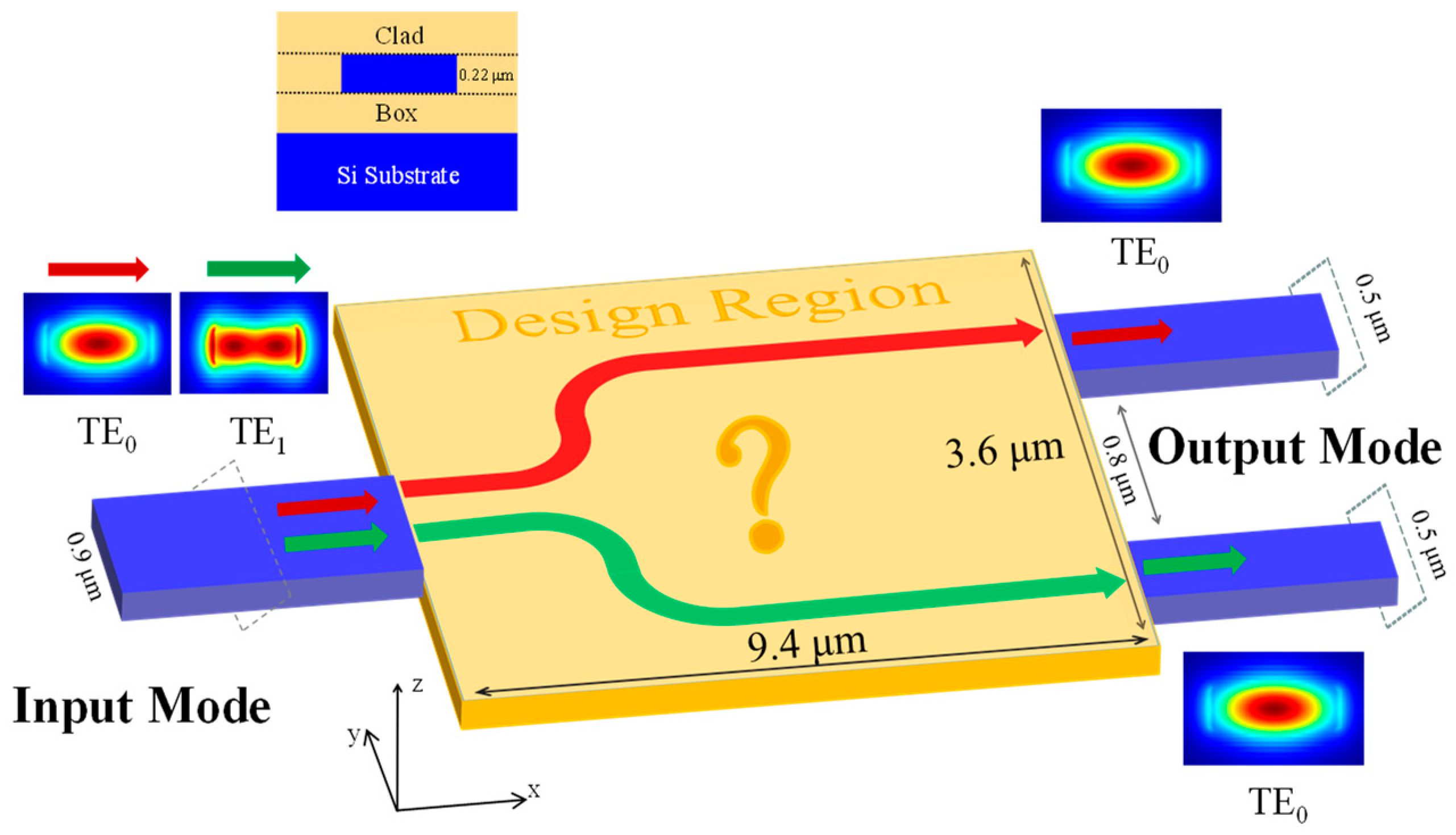
2.1. Design Target
2.2. Adjoint Method
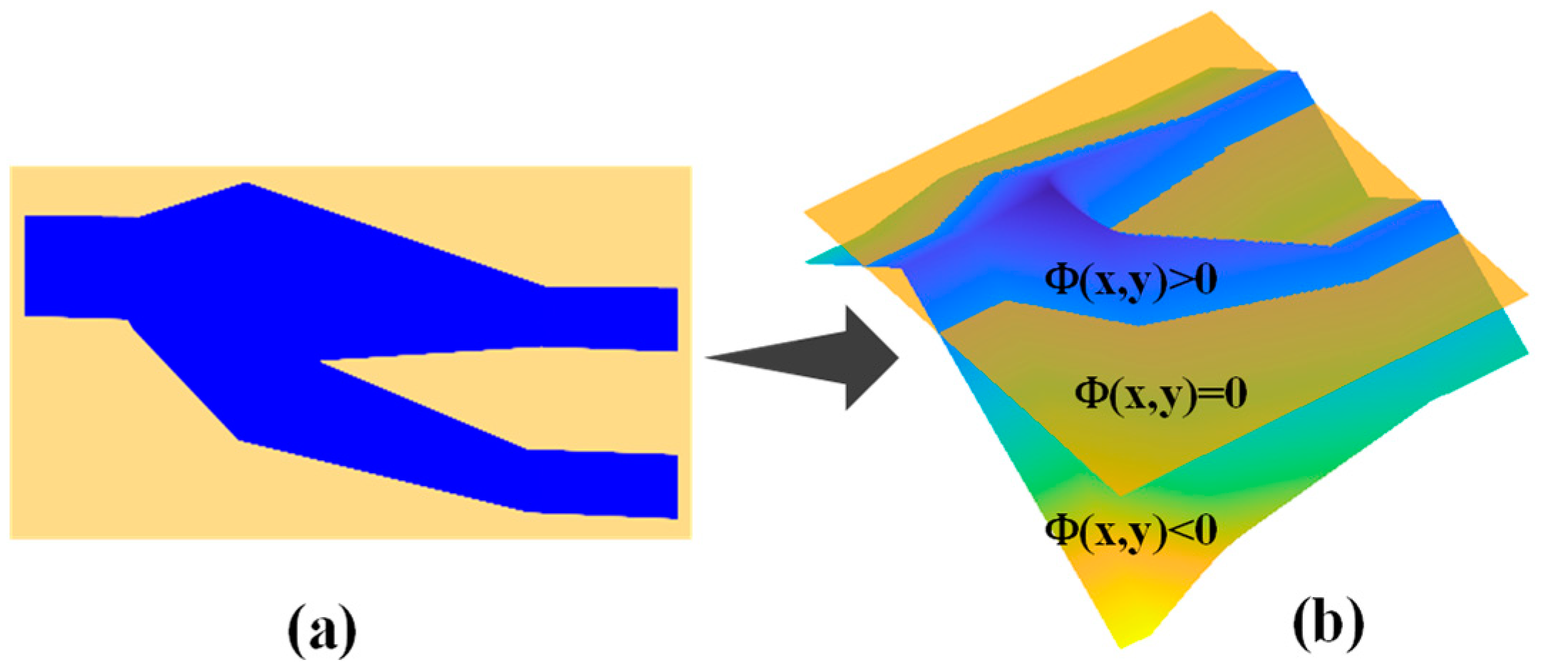
2.3. Level Set Method
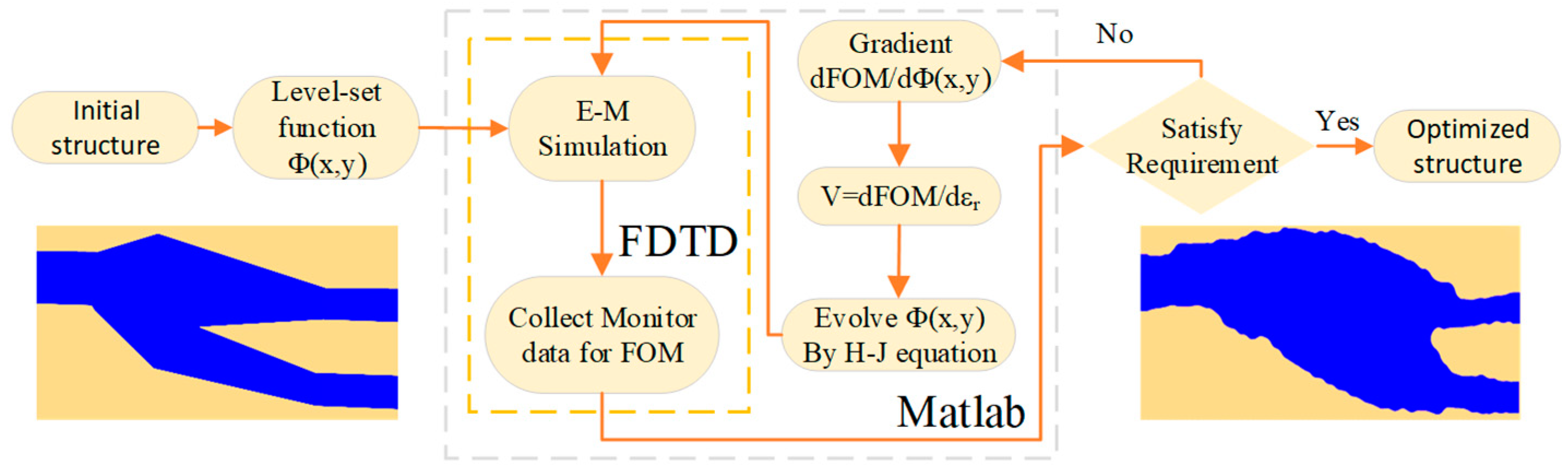
2.4. Optimization Process
3. Results
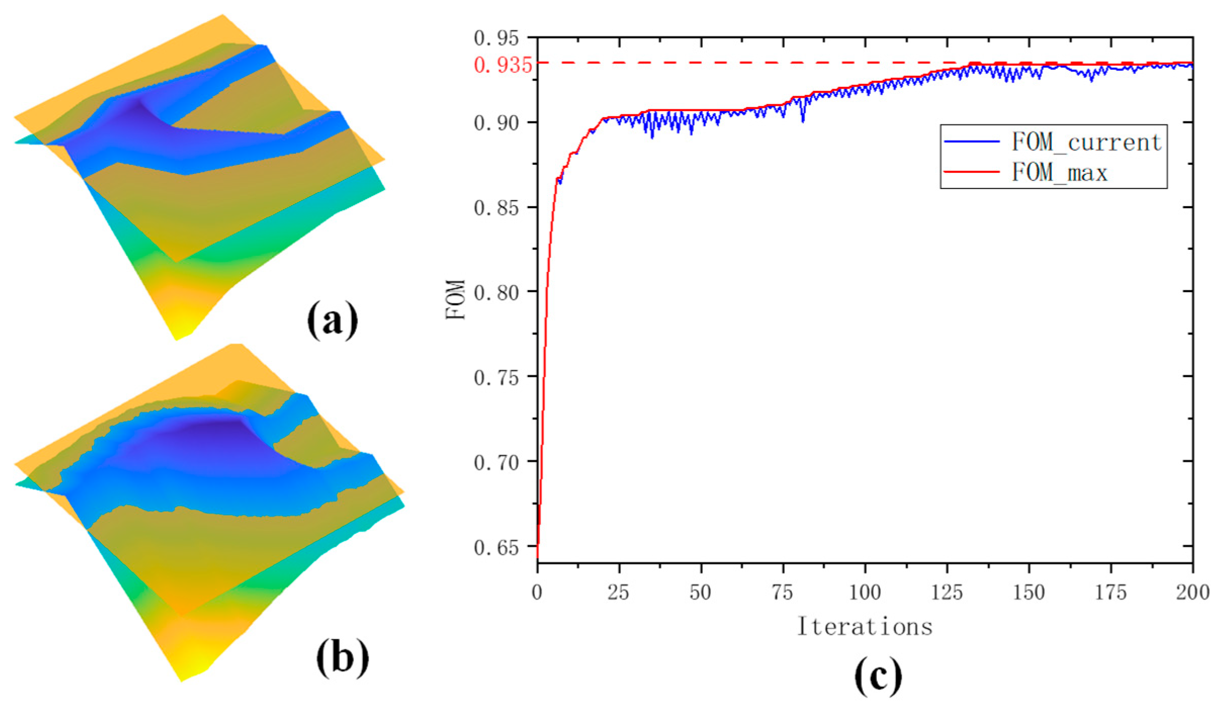
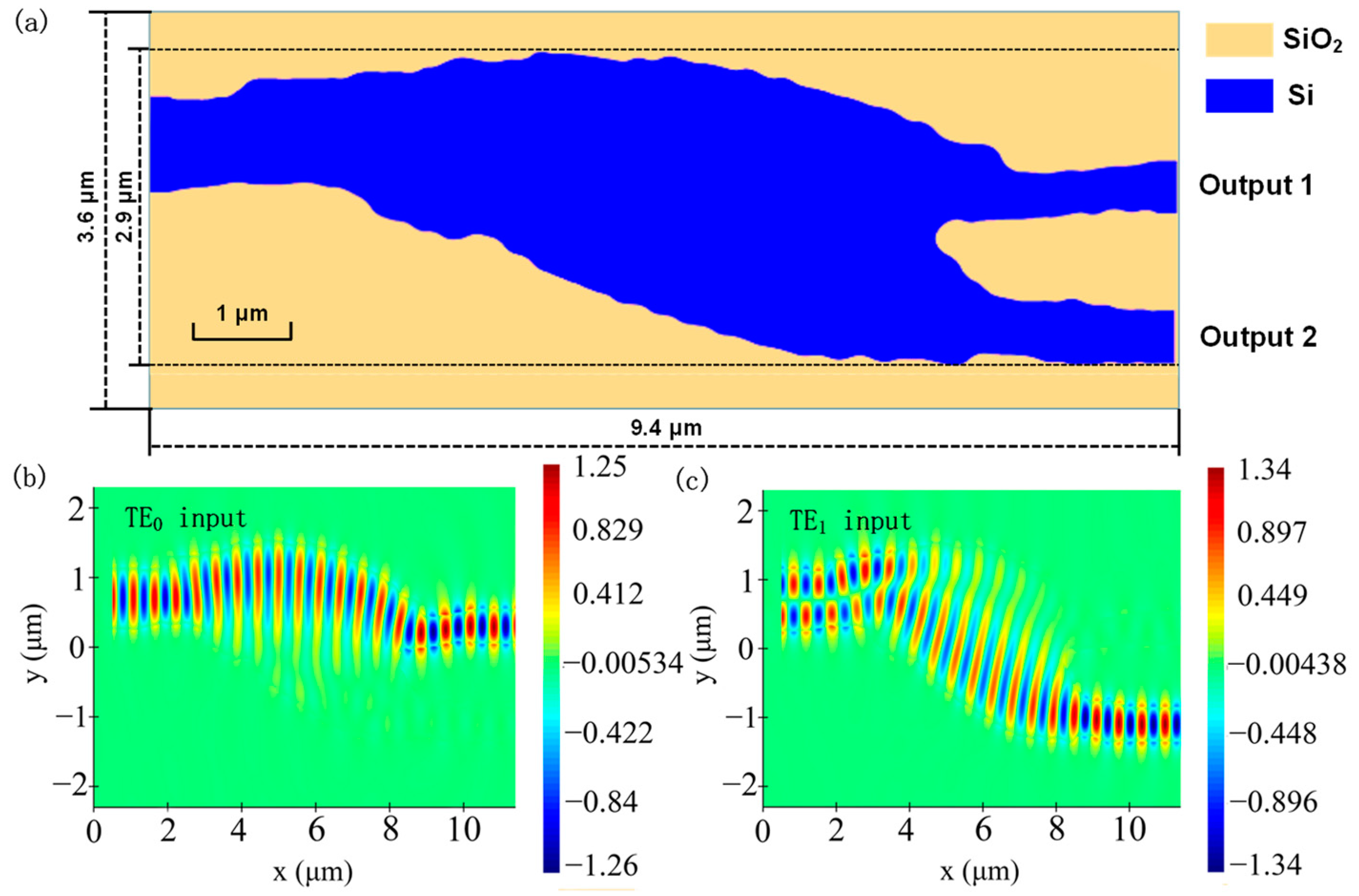
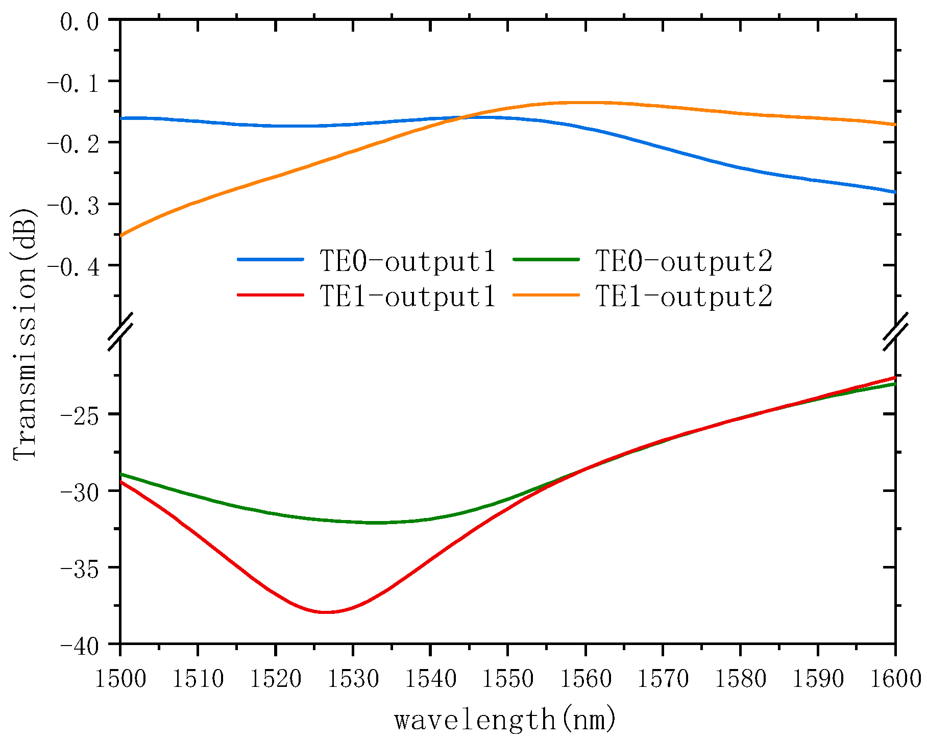
3.1. Simulation
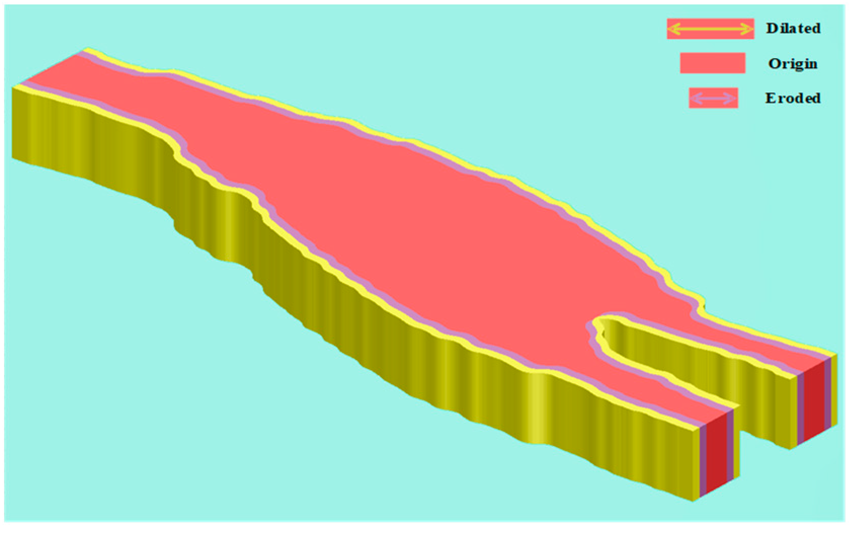
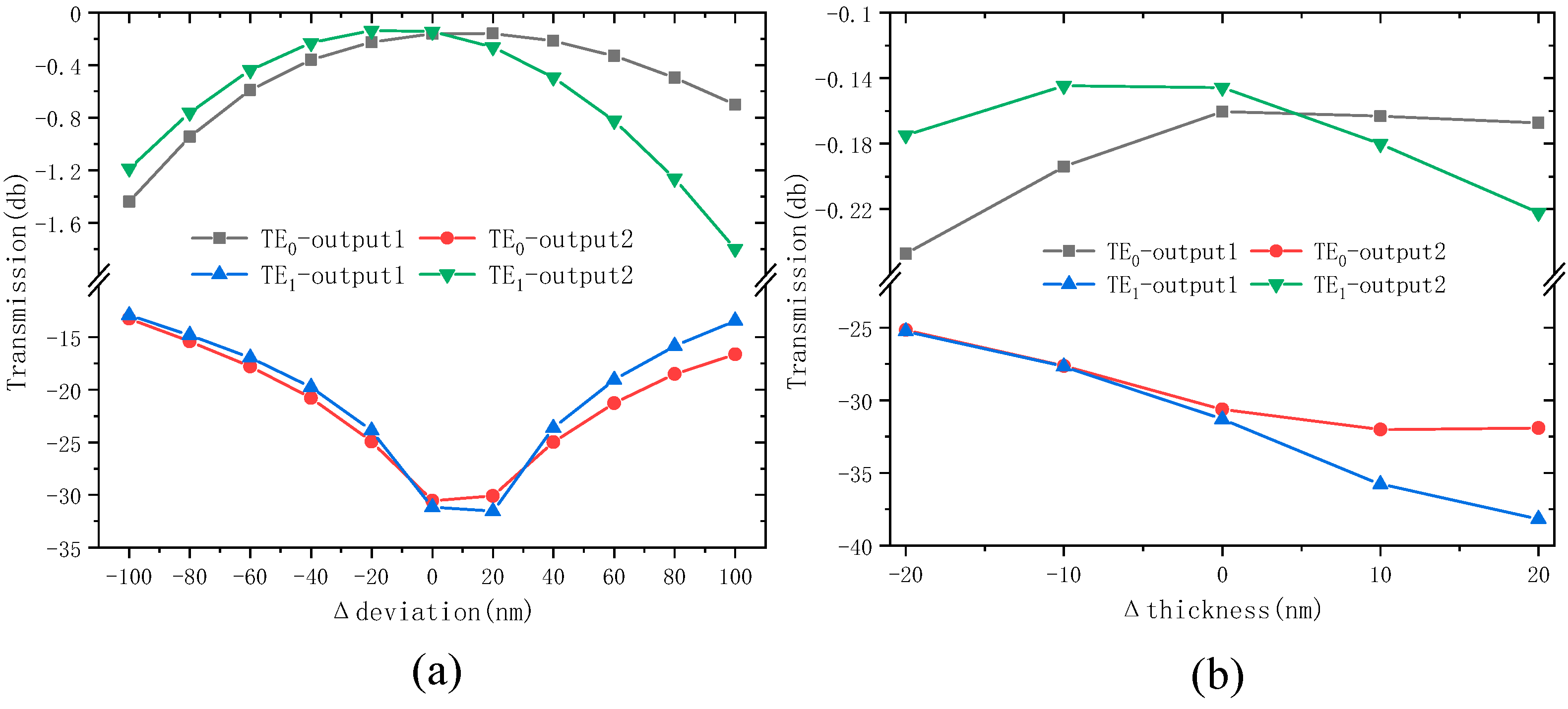
3.2. Fabrication Tolerance
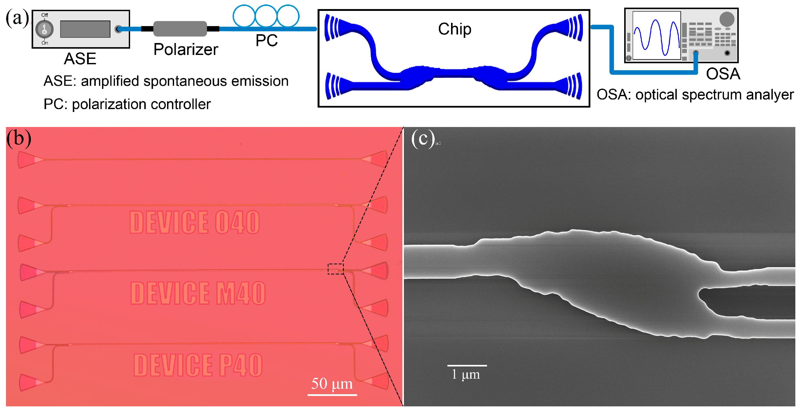
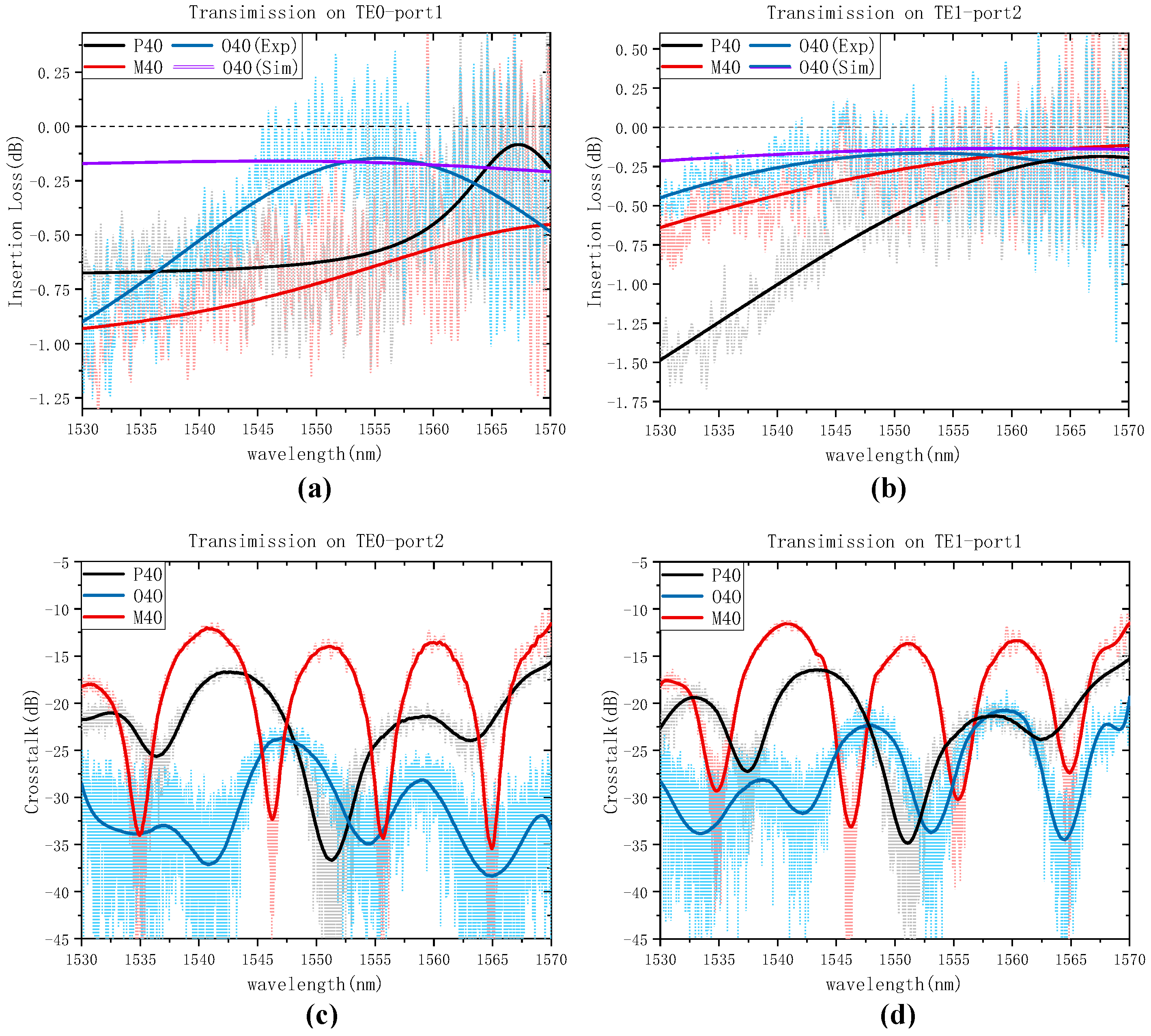
3.3. Experiment
4. Discussion
5. Conclusions
Author Contributions
Funding
Institutional Review Board Statement
Informed Consent Statement
Data Availability Statement
Conflicts of Interest
References
- Rahim, A.; Spuesens, T.; Baets, R.; Bogaerts, W. Open-Access Silicon Photonics: Current Status and Emerging Initiatives. Proc. IEEE 2018, 106, 2313–2330. [Google Scholar] [CrossRef]
- Bogaerts, W.; Chrostowski, L. Silicon Photonics Circuit Design: Methods, Tools and Challenges. Laser Photon. Rev. 2018, 12, 29. [Google Scholar] [CrossRef]
- Jin, M.; Wei, Z.Y.; Meng, Y.F.; Shu, H.W.; Tao, Y.S.; Bai, B.W.; Wang, X.J. Silicon-Based Graphene Electro-Optical Modulators. Photonics 2022, 9, 19. [Google Scholar] [CrossRef]
- Wang, S.; Chen, B.; Liang, R.; Liu, L.; Gao, M.; Wu, J.; Ho, P.-H. Energy-Efficient Resource Sharing Offloading Schemes for Collaborative Edge-Cloud Computing in Optical-Wireless Networks. In Proceedings of the 2022 27th OptoElectronics and Communications Conference (OECC) and 2022 International Conference on Photonics in Switching and Computing (PSC), Toyama, Japan, 3–6 July 2022; pp. 1–3. [Google Scholar]
- Brown, K.A.; Brittman, S.; Maccaferri, N.; Jariwala, D.; Ceano, U. Machine Learning in Nanoscience: Big Data at Small Scales. Nano Lett. 2020, 20, 2–10. [Google Scholar] [CrossRef] [PubMed]
- Piggott, A.Y.; Lu, J.; Lagoudakis, K.G.; Petykiewicz, J.; Babinec, T.M.; Vuckovic, J. Inverse design and demonstration of a compact and broadband on-chip wavelength demultiplexer. Nat. Photonics 2015, 9, 374–377. [Google Scholar] [CrossRef]
- Su, L.; Piggott, A.Y.; Sapra, N.V.; Petykiewicz, J.; Vuckovic, J. Inverse Design and Demonstration of a Compact on-Chip Narrowband Three-Channel Wavelength Demultiplexer. ACS Photonics 2018, 5, 301–305. [Google Scholar] [CrossRef]
- Muhieddine, K.; Lupu, A.; Cassan, E.; Lourtioz, J.M. Proposal and analysis of narrow band transmission asymmetric directional couplers with Bragg grating induced phase matching. Opt. Express 2010, 18, 23183–23195. [Google Scholar] [CrossRef] [PubMed]
- Paredes, B.; Mohammed, Z.; Villegas, J.; Rasras, M. Dual-Band (O & C-Bands) Two-Mode Multiplexer on the SOI Platform. IEEE Photonics J. 2021, 13, 9. [Google Scholar] [CrossRef]
- Jia, H.; Fu, X.; Zhou, T.; Zhang, L.; Yang, S.L.; Yang, L. Mode-selective modulation by silicon microring resonators and mode multiplexers for on-chip optical interconnect. Opt. Express 2019, 27, 2915–2925. [Google Scholar] [CrossRef]
- Gao, Y.; Xu, Y.; Ji, L.T.; Sun, X.Q.; Wang, F.; Wang, X.B.; Wu, Y.D.; Zhang, D.M. Scalable compact mode (de)multiplexer based on asymmetric Y-junctions. Opt. Commun. 2019, 438, 34–38. [Google Scholar] [CrossRef]
- Guo, F.; Lu, D.; Zhang, R.K.; Wang, H.T.; Liu, S.T.; Sun, M.D.; Kan, Q.; Ji, C. An MMI-Based Mode (DE)MUX by Varying the Waveguide Thickness of the Phase Shifter. IEEE Photonics Technol. Lett. 2016, 28, 2443–2446. [Google Scholar] [CrossRef]
- Tran, A.T.; Truong, D.C.; Nguyen, H.T.; Vu, Y.V. A new simulation design of three-mode division (de)multiplexer based on a trident coupler and two cascaded 3 × 3 MMI silicon waveguides. Opt. Quantum Electron. 2018, 50, 15. [Google Scholar] [CrossRef]
- Jafari, Z.; Zarifkar, A.; Miri, M. Compact fabrication-tolerant subwavelength-grating-basedtwo-mode division (de)multiplexer. Appl. Opt. 2017, 56, 7311–7319. [Google Scholar] [CrossRef] [PubMed]
- Molesky, S.; Lin, Z.; Piggott, A.Y.; Jin, W.L.; Vuckovic, J.; Rodriguez, A.W. Inverse design in nanophotonics. Nat. Photonics 2018, 12, 659–670. [Google Scholar] [CrossRef]
- Christiansen, R.E.; Sigmund, O. Inverse design in photonics by topology optimization: Tutorial. J. Opt. Soc. Am. B Opt. Phys. 2021, 38, 496–509. [Google Scholar] [CrossRef]
- Chen, W.W.; Li, H.X.; Zhang, B.H.; Wang, P.J.; Dai, S.X.; Liu, Y.X.; Li, J.; Li, Y.; Fu, Q.; Dai, T.G.; et al. Silicon Mode (de)Multiplexer Based on Cascaded Particle-Swarm-Optimized Counter-Tapered Couplers. IEEE Photonics J. 2021, 13, 11. [Google Scholar] [CrossRef]
- Chang, W.J.; Lu, L.L.Z.; Ren, X.S.; Li, D.Y.; Pan, Z.P.; Cheng, M.F.; Liu, D.M.; Zhang, M.M. Ultra-compact mode (de) multiplexer based on subwavelength asymmetric Y-junction. Opt. Express 2018, 26, 8162–8170. [Google Scholar] [CrossRef]
- Jiang, W.; Mao, S.; Hu, J. Inverse-designed counter-tapered coupler based broadband and compact silicon mode multiplexer/demultiplexer. Opt. Express 2023, 31, 33253–33263. [Google Scholar] [CrossRef]
- Mao, S.Q.; Hu, J.Z.; Jiang, W.F. Inverse Designed Silicon Mode Converters Based on the Direct Binary Search Algorithm. In Proceedings of the 14th IEEE International Conference on Advanced Infocomm Technology (ICAIT), Chongqing, China, 8–11 July 2022; pp. 243–246. [Google Scholar]
- Fujisawa, T.; Mitarai, T.; Okimoto, T.; Kono, N.; Fujiwara, N.; Sato, T.; Yagi, H.; Saitoh, K. Bayesian design of mosaic-based mode multiplexers for various wavelength bands. Opt. Express 2023, 31, 26842–26853. [Google Scholar] [CrossRef]
- Chang, W.; Zhang, M.; Lu, L.; Zhou, F.; Li, D.; Pan, Z.; Liu, D. Inverse design of an ultra-compact mode (de) multiplexer based on subwavelength structure. In Proceedings of the CLEO: Science and Innovations, San Jose, CA, USA, 14–19 May 2017; p. SF1J. 8. [Google Scholar]
- Frellsen, L.F.; Ding, Y.H.; Sigmund, O.; Frandsen, L.H. Topology optimized mode multiplexing in silicon-on-insulator photonic wire waveguides. Opt. Express 2016, 24, 16866–16873. [Google Scholar] [CrossRef]
- Wang, Y.R.; Li, J.; Wang, M.C.; Zhang, S.H.; Liu, Y.M.; Ye, H. Waveguide-integrated digital metamaterials for wavelength, mode and polarization demultiplexing. Opt. Mater. 2021, 122, 8. [Google Scholar] [CrossRef]
- Yang, S.L.; Jia, H.; Zhang, L.; Dai, J.C.; Fu, X.; Zhou, T.; Zhang, G.L.; Yang, L. Gradient-probability-driven discrete search algorithm for on-chip photonics inverse design. Opt. Express 2021, 29, 28751–28766. [Google Scholar] [CrossRef] [PubMed]
- Wang, K.; Ren, X.; Chang, W.; Lu, L.; Liu, D.; Zhang, M.J.P.R. Inverse design of digital nanophotonic devices using the adjoint method. Photon. Res. 2020, 8, 528–533. [Google Scholar] [CrossRef]
- Ruan, X.K.; Li, H.; Chu, T. Inverse-Designed Ultra-Compact Polarization Splitter-Rotator in Standard Silicon Photonic Platforms With Large Fabrication Tolerance. J. Light. Technol. 2022, 40, 7142–7149. [Google Scholar] [CrossRef]
- Ambrosio, L.; Dal Maso, G. A general chain rule for distributional derivatives. Proc. Math. Am. Soc. 1990, 108, 691–702. [Google Scholar] [CrossRef]
- Lalau-Keraly, C.M.; Bhargava, S.; Miller, O.D.; Yablonovitch, E. Adjoint shape optimization applied to electromagnetic design. Opt. Express 2013, 21, 21693–21701. [Google Scholar] [CrossRef]
- Van Dijk, N.P.; Maute, K.; Langelaar, M.; van Keulen, F. Level-set methods for structural topology optimization: A review. Struct. Multidiscip. Optim. 2013, 48, 437–472. [Google Scholar] [CrossRef]
- Gostimirovic, D.; Masnad, M.M.; Xu, D.X.; Grinberg, Y.; Liboiron-Ladouceur, O. Pre-Fabrication Performance Verification of a Topologically Optimized Mode Demultiplexer using Deep Neural Networks. In Proceedings of the European Conference on Optical Communication (ECOC), Basel, Switzerland, 18–22 September 2022. [Google Scholar]


| Method | Modes | Simulation IL (dB) | Experiment IL (dB) | Experiment CT (dB) | Ref. |
|---|---|---|---|---|---|
| Direct binary search | TE0; TE1 | <0.47 (1530–1590 nm) | <1.0 (1530–1590 nm) | <−24 | [18] |
| TE0; TE1 | <1.53 (150 nm in C-band) | <3.0 (138 nm in C-band) | <−18.6 | [19] | |
| TE0; TE1 | <0.83 (1500–1630 nm) | <1.7 (1525–1565 nm) | <−10.91 | [20] | |
| Density topology optimization | TE0; TE1 | - | <1.5 (1530–1600 nm) | <−25 | [22] |
| TE0; TE1; TE2 | <1.2 (1520–1620 nm) | <3.0 (1520–1620 nm) | <−12 | [23] | |
| TE0; TE1 | <2.6 (1520–1580 nm) | - | - | [24] | |
| TE0; TE1 | <0.63 (the whole O-band) | - | - | [27] | |
| Bayesian DBS | TE0; TE1 | <0.9 (1270–1330 nm) <1.1 (1530–1570 nm) | <4.2 (1270–1330 nm) <3.4 (1530–1570 nm) | <−22 <−13 | [21] |
| Gradient-probability-driven search algorithm | TE0; TE1 | <1.0 (1525–1610 nm) | - | - | [25] |
| Digitized adjoint method | TE0; TE1 | Avg. 0.68 (1530–1570 nm) | <1.36 (1530–1570 nm) | <−20 | [26] |
| Adjoint and level set method | TE0; TE1 | <0.35 (1500–1600 nm) | <0.89 (1530–1570 nm) | <−24 | This work |
Disclaimer/Publisher’s Note: The statements, opinions and data contained in all publications are solely those of the individual author(s) and contributor(s) and not of MDPI and/or the editor(s). MDPI and/or the editor(s) disclaim responsibility for any injury to people or property resulting from any ideas, methods, instructions or products referred to in the content. |
© 2024 by the authors. Licensee MDPI, Basel, Switzerland. This article is an open access article distributed under the terms and conditions of the Creative Commons Attribution (CC BY) license (https://creativecommons.org/licenses/by/4.0/).
Share and Cite
Zheng, H.; Yang, S.; Yu, Y.; Zhang, L. Compact SOI Dual-Mode (De)multiplexer Based on the Level Set Method. Appl. Sci. 2024, 14, 426. https://doi.org/10.3390/app14010426
Zheng H, Yang S, Yu Y, Zhang L. Compact SOI Dual-Mode (De)multiplexer Based on the Level Set Method. Applied Sciences. 2024; 14(1):426. https://doi.org/10.3390/app14010426
Chicago/Turabian StyleZheng, Han, Shanglin Yang, Yue Yu, and Lei Zhang. 2024. "Compact SOI Dual-Mode (De)multiplexer Based on the Level Set Method" Applied Sciences 14, no. 1: 426. https://doi.org/10.3390/app14010426