1. Introduction
GaSb-based lasers are the most promising candidates among mid-infrared lasers owing to their high efficiency, small volume, and low cost, which are in high demand for gas detection [
1], pollution monitoring [
2], aesthetic surgery [
3], material processing [
4], and resonant pumping of the Ho-doped host [
5]. Radiation recombination in InGaAsSb/AlGaAsSb type-I quantum wells offers output radiation with wavelengths covering 2~3 μm and exhibits higher efficiency and temperature stability than that in InP-based quantum wells. To achieve high output power, a broad-area ridge waveguide is the normally used structure in electrically pumped diode lasers. Benefiting from the flexibility of the energy band design and precise MBE material growth techniques, both wide wavelength coverage and room-temperature continuous-wave operation have been achieved in GaSb-based broad-area lasers.
In order to achieve high-power, high-efficiency output performance, an optimized separate confinement heterostructure (SCH) design [
6], a narrow waveguide layer with an optimized doping profile [
7], an asymmetric waveguide layer with a carrier barrier [
8], and cascade type-I quantum wells [
9] have been attempted and resulted in a low threshold, low internal loss, and Watt-level high-output-power InGaAsSb/AlGaAsSb quantum-well lasers. Except for cascade type-I quantum-well lasers, the abovementioned schemes are made of composition-fixed functional layers, which limits the design flexibility of GaSb-based lasers.
The composition-graded layer was first proposed in the GaAs/AlGaAs system, which is known as a graded-index separate confinement heterostructure (GRIN SCH) and has been well developed in InP and GaN systems [
10,
11,
12,
13]. The composition-graded layer epitaxy technique provides more flexibility for semiconductor device designs, e.g., the modification of the built-in electric field, bandgap profile, and refractive index profile [
14,
15,
16]. Further improving the performance of GaSb-based lasers requires addressing the series resistance caused by the abrupt interface between the waveguide layer and cladding layer, which remains a severe problem. On the one hand, series resistance causes power dissipation, and on the other hand, it accelerates heat accumulation, which lowers efficiency. Inserting a composition-graded layer into lasers can reduce the series resistance induced by a discontinuous bandgap and enhance the built-in electric field to raise the carrier injection efficiency [
17].
For GaSb-based lasers, the composition-graded AlGaAsSb layer between the high-Al-content AlGaAsSb cladding layer and low-Al-content AlGaAsSb waveguide layer is supposed to maintain the lattice constant throughout the content regulation process. Composition-graded AlGaAsSb layer preparation is impeded by the two following facts: group V element competition makes the As incorporation behavior unclear, and the lattice constant is far more composition-dependent than GaAa/AlGaAs, whose lattice constant is almost independent of Al content. This difficulty also exists in InP-based devices with an InGaAsP composition-graded layer; conventional epitaxy processes divide the composition-graded region into thin sublayers, and each sublayer is grown with lattice-matched parameters to obtain the required composition profiles. However, such composition-graded epitaxy technology is more applicable to MOCVD, where source adjustment needs less response time, while GaSb-based device epitaxy is mainly accomplished in MBE systems. Growth interruption for changing and stabilizing the cell temperature may cause residual impurity incorporation for MBE [
18]. A more competitive alternative is dominating beam equivalent pressure by precisely controlling the cell temperature and valve position to implement continuous growth. A continuously graded parabolic quantum-well laser was produced with such a method in the GaAs/AlGaAs system [
19,
20]. Such a method has not been discussed in detail in GaSb-based systems.
In this work, we put forward a novel composition-graded AlGaAsSb layer growth method by precisely controlling the group Ⅲ cell temperature and group Ⅴ cell valve position. Based on the analysis of the AlGaAsSb preparation features and MBE cell characteristics, we prepared a composition-graded AlGaAsSb layer sample. AFM and HRXRD results indicate that the AlGaAsSb composition modulation difficulty is overcome, and GaSb-lattice-matched, high-quality composition-graded AlGaAsSb layer epitaxy is achieved. Lasers adopting the composition-graded layer exhibit a high output power of 1.8 W, with a maximum power conversion efficiency of 28%. A high internal quantum efficiency of 83% is also maintained even at 40 °C, and the low internal loss of 4~5 cm−1 shows little temperature dependence. A bar with the same epitaxial structure realized a record-high 18 W output power. Our research provides more flexibility for GaSb-based laser design.
2. Composition-Graded AlGaAsSb Layer Epitaxy
In this work, composition-graded AlGaAsSb layers were inserted between an Al0.25Ga0.75As0.02Sb0.98 waveguide layer and an Al0.5Ga0.5As0.04Sb0.96 cladding layer. There is a bandgap difference of ~0.3 eV between Al0.25Ga0.75As0.02Sb0.98 and Al0.5Ga0.5As0.04Sb0.96. The composition-graded AlGaAsSb layer is supposed to be beneficial to the electrical characteristics and efficiency of lasers.
According to Vegard’s law [
21], the AlGaAsSb lattice constant is expressed as:
where
is 5.6611 Å,
is 6.1355 Å,
is 5.6533 Å, and
is 6.0959 Å. Linear interpolation Equation (1) is visualized in
Figure 1. A 1% Al content deviation from the GaSb-lattice-matched condition will cause a 65 ppm lattice mismatch, and the same deviation for As content will lead to a 750 ppm lattice mismatch. A strict lattice match is unnecessary for thick-layer epitaxy. Maintaining a lattice mismatch within 1000 ppm is sufficient to effectively prevent dislocation generation. The line segment connecting Al
0.25Ga
0.75As
0.02Sb
0.98 and Al
0.5Ga
0.5As
0.04Sb
0.96 represents the ideal composition modulation process throughout composition-graded AlGaAsSb layer epitaxy, and the actual composition modulation process with a deviation within the marked acceptable region can also result in high-quality AlGaAsSb epitaxy. As
Figure 1 illuminates, the Al content fluctuation is acceptable on the condition that the deviation from the designed value is less than 16%, and the As content fluctuation within 1.3% is acceptable. Therefore, precise As content control is much more essential for GaSb-lattice-matched AlGaAsSb quaternary epitaxy.
While group Ⅲ elements with unit sticking coefficients are capable of being directly compositionally modified by adjusting the growth rate, the control of group V element incorporation is more complicated. Materials grown by MBE are usually in group V overpressure conditions, which means that group V elements are in excess of the available surface group V vacancies, causing their sticking coefficients to be less than one unit. The consequent group V competition for incorporation in mixed-anion semiconductor alloys causes difficulty in group V content control [
22]. Considering that group V element incorporation is sensitive to group V flux and growth temperature, we kept the growth temperature, group Ⅲ flux, and Sb flux constant and vary the As cell valve position to determine the GaSb-lattice-matched AlGaAsSb epitaxy condition in the following experiment.
A linear relationship between the As content of AlGaAsSb and the As beam equivalent pressure (BEP) in low-As-content conditions has been reported [
23]. An experiment was conducted to determine the As BEP dependence of As content in our equipment. The substrate temperature was calibrated by the 2 × 5 → 1 × 3 reconstruction transition of the GaSb surface, which is set as Tc, according to RHEED observations, and the growth temperature is 130 °C above Tc for high-quality AlGaAsSb epitaxy. The lattice mismatch was experimentally deduced from the HRXRD diffraction peak position difference of the epitaxial layer and substrate, according to Equation (2) [
24].
where
is the diffraction angle of the substrate, and
is the diffraction angle of the epitaxial layer.
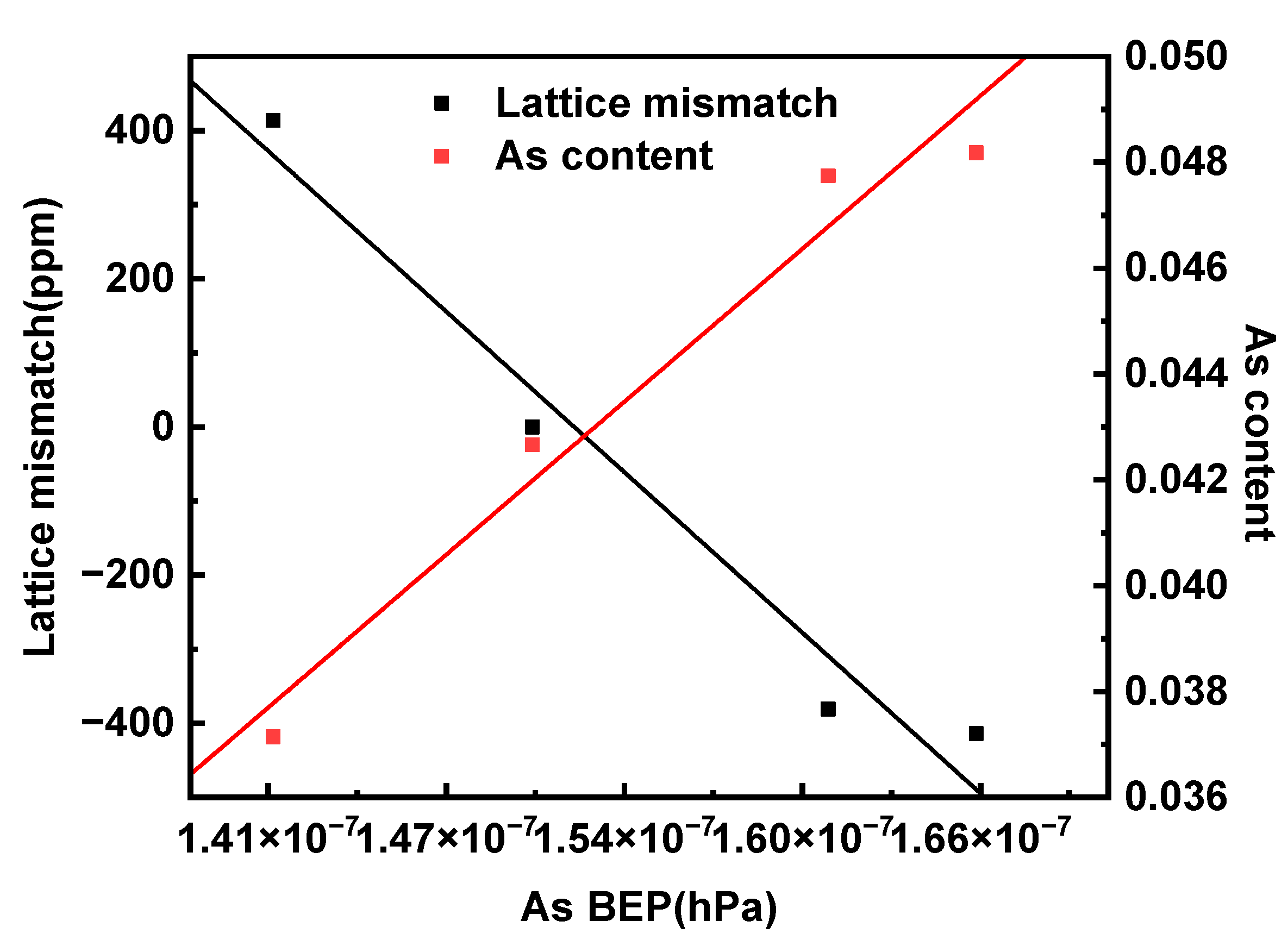
Figure 2 shows how the As BEP influences As incorporation when the Al and Ga growth rates are both 0.5 ML/s. When the As BEP varies from 1.40 × 10
−7 hPa to 1.67 × 10
−7 hPa, the lattice mismatch is maintained within ±500 ppm. A quasi-linear dependence of As content on the As BEP is observed, and the slope is about 0.0045/1 − 10
8 hPa, which reveals a constant As stacking coefficient within the researched As BEP range. The experiment was conducted under Sb overpressure (1.33 × 10
−6 hPa), where Sb BEP has little influence on the As content and group Ⅲ composition does not enhance As incorporation [
25]. Therefore, it is reasonable to assume a constant As stacking coefficient throughout the composition-graded AlGaAsSb layer epitaxy process.
Valved cracker cells overcome the flux instability by providing a large reservoir of group V element vapor and controlling the flux with a needle valve. Real-time As flux monitoring and feedback control have been demonstrated by taking advantage of the rapid and repeatable flux response to the valve position [
26]. In group V element composition-varying conditions, a step-like flux sequence is usually adopted to obtain the designed composition profile [
27]. In this work, As BEP quasi-linear variation was accomplished by ramping the As cracker valve position to prevent background impurity incorporation induced by growth interruption. The As BEP is monitored by an ion gauge installed in the growth chamber.
Figure 3 illustrates the As BEP profile obtained by ramping up the As valve position. The As BEP’s linearly ascending segment lasts for ~830 s, corresponding to the valve position ramp-up procedure. The valve position is fixed after the As BEP reaches the setpoint, and the As BEP is maintained for subsequent high-Al-content AlGaAsSb epitaxy. According to
Figure 2, an 800 ppm lattice mismatch is the outcome of a 2.67 × 10
−8 hPa As BEP deviation. Since an As BEP deviation within 2.67 × 10
−8 hPa is acceptable for lattice-matched epitaxy, the demonstrated As BEP profile can be considered a linear modulation procedure, which is functional for composition-graded AlGaAsSb layer epitaxy.
Group Ⅲ element diffusion cells show different operating characteristics from group V valved cracker cells: the group Ⅲ element flux is directly produced by metal evaporation, which causes an exponential flux–temperature dependence in the steady-state case, and flux transients occur when the cell operating condition changes. In addition, cell temperature ramping is not as rapid as valve position ramping. However, Rouel demonstrated linear Ga growth rate modulation with a rate of change of 12.4 (Å/h)/s by linearly ramping the Ga cell temperature [
28], indicating that the linear modification of group Ⅲ BEP is feasible by adopting a sufficiently slow ramping rate. A similar approach was taken in our experiment, and
Figure 4 shows the flux obtained in the Al temperature time-varying growth. The Al cell temperature ramp-up procedure lasts for ~830 s, and the cell temperatures of the starting and finishing points are calibrated in advance from the RHEED oscillation curve for the specified Al growth rate, namely, 0.16 ML/s for Al
0.25Ga
0.75As
0.02Sb
0.98 and 0.5 ML/s for Al
0.5Ga
0.5As
0.04Sb
0.96. Linear Al flux modulation followed by flux fluctuation as the cell temperature reaches the setpoint is observed. Therefore, the Al shutter should be closed as soon as the composition-graded layer growth is over to avoid the influence of an Al temperature overshoot, and an interruption is necessary for temperature stabilization.
Based on the abovementioned linear Al and As flux modulation experiment, we can estimate the thickness of the composition-graded layer by using Equation (3). The Al growth rate is assumed to vary linearly with time, and GaSb-lattice-matched growth is guaranteed by As BEP modulation.
where d is the thickness of the composition-graded layer,
T is the duration of the growth process,
A is a constant depending on the lattice of the GaSb substrate, and
a is the ramp rate of the Al growth rate. In our linear Al modulation experiment,
a was set to 4.4 (Å/h)/s to obtain quasi-equilibrium growth. A thickness of 210 nm and a growth duration of 827 s can be obtained, according to Equation (3), when the Ga growth rate is set to 0.5 ML/s and the Al growth rate ramps from 0.16 ML/s to 0.5 ML/s.
A composition-graded layer sample was grown by adopting linear As and Al BEP modification parameters. The sample consisted of a 210 nm composition-graded AlGaAsSb layer and a 10 nm GaSb cap layer. The Al content varied linearly from 0.25 to 0.5 in the composition-graded layer. The sample was characterized by AFM and HRXRD, the results are illustrated in
Figure 5. In the 10 μm × 10 μm AFM scanning result, clear atomic steps and 1.7 Å RMS surface roughness indicate high epitaxial quality. A single sharp HRXRD peak implies lattice-matching growth. Similar procedures were adopted to verify the Al
0.5Ga
0.5As
0.04Sb
0.96 to Al
0.25Ga
0.75As
0.02Sb
0.98 composition-graded layer. The AFM and HRXRD results also suggest high-quality and GaSb-lattice-matching growth.
3. Laser Performance
The verified composition-graded layer was then applied to InGaSb/AlGaAsSb quantum-well lasers. As
Figure 6 shows, the laser consists of a 1500 nm Al
0.5Ga
0.5As
0.04Sb
0.96: Te bottom cladding layer, a 210 nm Al
0.5Ga
0.5As
0.04Sb
0.96 to Al
0.25Ga
0.75As
0.02Sb
0.98 bottom composition-graded layer, a 270 nm Al
0.25Ga
0.75As
0.02Sb
0.98 bottom waveguide layer, a 40 nm active region, a 270 nm Al
0.25Ga
0.75As
0.02Sb
0.98 top waveguide layer, a 210 nm Al
0.25Ga
0.75As
0.02Sb
0.98 to Al
0.5Ga
0.5As
0.04Sb
0.96 top composition-graded layer, a 2000 nm Al
0.5Ga
0.5As
0.04Sb
0.96: Be top cladding layer, and a 250 nm GaSb: Be contact layer. The active region includes two 10 nm In
0.2Ga
0.8Sb quantum wells, which are separated by a 20 nm Al
0.25Ga
0.75As
0.02Sb
0.98 barrier.
GaSb-lattice-matched AlGaAsSb transforms from a direct bandgap semiconductor to an indirect bandgap semiconductor when the Al content is higher than 0.45. Electrons injected from the Al0.5Ga0.5As0.04Sb0.96 cladding layer first localize in the X valley and are then scattered into the Γ valley while being transported through the composition-graded AlGaAsSb layer, which is smoother than electrons crossing the abrupt Al0.5Ga0.5As0.04Sb0.96/Al0.25Ga0.75As0.02Sb0.98 interface. In addition, composition-graded AlGaAsSb layers flatten the potential barrier peak of the heterostructure, lower the series resistance, and suppress the rectification effect caused by the potential barrier peak.
A 200 μm wide ridge pattern was prepared via the photolithography process and then etched 2 μm deep in an inductively coupled plasma reactive-ion etching (ICP-RIE) system. A 250 nm thick SiO2 insulation layer was deposited on the ridge waveguide by plasma-enhanced chemical vapor deposition (PECVD), through which a 190 μm wide current injection window was etched by reactive-ion etching (RIE). The GaSb substrate was then thinned and polished to 120 μm thickness to reduce the series resistance. AuGeNi/Au and TiPtAu were sputtered as N contact metal and P contact metal, respectively. After the deposition of AuGeNi/Au, rapid thermal processing (RTP) was conducted to form Ohmic contact. A wafer was then cleaved into bars with different cavity lengths for subsequent experiments. Single emitters were p-side-down c-mounted on a copper heatsink with In solder, while bar lasers were mounted onto a microchannel heatsink for better heat dissipation performance. The tests were all conducted in CW or QCW (with a pulse duration of 100 μs at a 100 Hz repetition rate) operation.
For CW output performance characterization, bars with 1 mm cavity length were 5% anti-reflection- and 95% high-reflection-coated and then cleaved into 500 μm wide chips as single emitters. The CW performance at 15 °C of a single emitter is shown in
Figure 7. The turn-on voltage is 0.65 V. Since the wavelength of our laser is 2006 nm, the theoretical lowest turn-on voltage for population inversion is the quasi-Fermi energy difference corresponding to the lasing transition, which can be expressed as Equation (4) [
27]:
The difference between the turn-on voltage and this theoretical lowest value is the voltage penalty induced by heterojunction barriers [
29]. The low turn-on voltage demonstrates that the adoption of the composition-graded AlGaAsSb layer effectively reduces the voltage penalty and improves the performance of GaSb-based lasers. The threshold current is 230 mA, corresponding to a threshold current density of 121 A/cm
2. Excellent threshold parameters, e.g., a low turn-on voltage and a low threshold current density, ensure the high-efficiency operation of our lasers.
The potential barrier peak of the Al
0.5Ga
0.5As
0.04Sb
0.96/Al
0.25Ga
0.75As
0.02Sb
0.98 heterojunction is flattened after the introduction of the composition-graded AlGaAsSb layer, and a low series resistance of 0.144 Ω is obtained. The slope efficiency decreases from ~0.32 W/A with the increasing operation current, which is caused by heat accumulation in the active region when lasers are characterized in CW operation. As the actual temperature of the active region rises, the threshold current for lasering rises and the internal quantum efficiency is reduced, resulting in a low power conversion efficiency [
30]. Due to the optimized mounting process, the heat generated in the lasers is dispersed quickly, ensuring a high slope efficiency in a wide operating current range and delaying output power saturation caused by thermal rollover. As a result, a high output power of 1.8 W is achieved at 8 A, while a high PCE of 28% is obtained at 1.1 A. Though PCE decreases with a higher current, it remains more than 12% at 8 A. The wavelength and FWHM of the laser operating at 3A are 2006 nm and 6.15 nm, respectively, since no additional longitudinal mode selection structure is adopted in our FP laser.
A 0.95 cm laser bar containing 19,500 μm wide emitters was 5% anti-reflection- and 95% high-reflection-coated and then mounted on a microchannel heatsink. Since the emitters in the laser bar are in parallel, the laser bar exhibits low-voltage, high-current, and high-power output performance. Nineteen emitters operating in parallel generate massive heat, and the heat distribution causes horizontal and perpendicular thermal stress in the laser bar and a consequent “smile” [
31]. A microchannel heatsink with low thermal resistance and high heat flux is utilized to relieve heat accumulation and thermal stress. The laser bar with a 40% fill factor is characterized in CW operation at 15 °C. The CW performance is plotted in
Figure 8. A record-high CW output power of 18 W is achieved at 75 A.
As expressed in Equation (5) [
32], internal loss and internal quantum efficiency were determined with 1 mm, 1.5 mm, and 2 mm long uncoated lasers.
where
is the total slope efficiency, which is 2 times the slope efficiency measured from a single facet,
q is the electric charge of a single electron,
is the energy of a single emitted photon,
is the internal loss of the laser,
L is the cavity length of the laser, and
and
are the reflectivity of each facet, which is ~35% for uncoated GaSb-based lasers. In order to eliminate the interference of heat accumulation with the laser efficiency, the characterization of emitters was conducted in QCW operation, and
was calculated according to the linear interval of the power–current relation near the lasering threshold.
The linear dependence of 1/
and cavity length is illustrated in
Figure 9. The intercept of the linear fitted line is proportional to the internal quantum efficiency, and the internal loss can be deduced from the slope of the fitted line. With higher carrier injection efficiency benefiting from the built-in electric field of the composition-graded AlGaAsSb layer, the lasers exhibit 83% internal quantum efficiency and 3.9 cm
−1 internal loss even at 40 °C. A low and almost temperature-independent internal loss of 4~5 cm
−1 is observed as the heatsink temperature rises from 5 °C to 45 °C, which indicates that free carrier absorption is effectively reduced in our lasers. A 270 nm thick Al
0.25Ga
0.75As
0.02Sb
0.98 waveguide layer and a 210 nm thick composition-graded AlGaAsSb layer on both sides of the active region lower the optical confinement factor of cladding layers. The temperature insensitivity of internal loss also suggests low free carrier absorption at a higher current injection level, which maintains high efficiency at a high operation current.
The characteristic temperatures
T0 and
T1, signifying the exponential temperature dependence of the threshold current and efficiency, are determined by using the following expressions [
33]:
where
and
are the ideal threshold current and slope efficiency at 0 K.
An uncoated single emitter with a 3 mm cavity length was c-mounted on a copper heatsink for power–current performance characterization. The heatsink temperature was controlled and varied from 5 °C to 45 °C with a thermoelectric cooler (TEC). The data used for the threshold current and slope efficiency calculations were extracted from the linear interval of the power–current relation near the lasering threshold to minimize the error induced by active region heating.
Figure 10 plots the temperature dependence of
and
when lasers were characterized in CW operation.
T0 and
T1 deduced from the slopes of linear fitted lines are ~61 K and ~213 K, respectively, while
T0 and
T1 deduced in QCW operation are ~67 K and ~224 K, respectively. The increase in the characteristic temperature is the consequence of heat removal, and an even higher characteristic temperature is expected when the experiment is conducted in PW operation. Sufficient carrier confinement to hinder carrier leakage caused by thermal carrier emission is essential for high-efficiency laser operation, and a high characteristic temperature confirms our design is an efficient structure.

 ,
, 


