Article

All-Digital Computing-in-Memory Macro Supporting FP64-Based Fused Multiply-Add Operation

1
Beijing Smartchip Microelectronics Technology Co., Ltd., Beijing 102299, China
2
School of Integrated Circuit Science and Engineering, Beihang University, Beijing 100191, China
*
Author to whom correspondence should be addressed.
Appl. Sci. 2023, 13(7), 4085; https://doi.org/10.3390/app13074085
Submission received: 29 January 2023 / Revised: 15 March 2023 / Accepted: 18 March 2023 / Published: 23 March 2023
(This article belongs to the Special Issue Advanced Circuits and Systems for Emerging Applications)

Abstract

:
Recently, frequent data movement between computing units and memory during floating-point arithmetic has become a major problem for scientific computing. Computing-in-memory (CIM) is a novel computing paradigm that merges computing logic into memory, which can address the data movement problem with excellent power efficiency. However, the previous CIM paradigm failed to support double-precision floating-point format (FP64) due to its computing complexity. This paper presents a novel all-digital CIM macro-DCIM-FF to complete FP64 based fused multiply-add (FMA) operation for the first time. With 16 sub-CIM cells integrating digital multipliers to complete mantissa multiplication, DCIM-FF is able to provide correct rounded implementations for normalized/denormalized inputs in round-to-nearest-even mode and round-to-zero mode, respectively. To evaluate our design, we synthesized and tested the DCIM-FF macro in 55-nm CMOS technology. With a minimum power efficiency of 0.12 mW and a maximum computing efficiency of 26.9 TOPS/W, we successfully demonstrated that DCIM-FF can run the FP64-based FMA operation without error. Compared to related works, the proposed DCIM-FF macro shows significant power efficiency improvement and less area overhead based on CIM technology. This work paves a novel pathway for high-performance implementation of an FP64-based matrix-vector multiplication (MVM) operation, which is essential for hyperscale scientific computing.

1. Introduction

In the era of pervasive high-performance computing, supercomputers have ever-growing computation capability and network bandwidth. The power and computing efficiency issues have become two of the primary concerns of hyperscale scientific computing due to the increasing computing precision and complexity of supercomputers. Limited by the traditional Von Neumann computing architecture, frequent data movement between computing units and memory during high-precision calculation has become a major problem for scientific computing, and a significant amount of time and energy is spent during the data movement. This computing architecture has become one of the main bottlenecks for high-performance low-power computing systems in hyperscale scientific computing [1,2,3].
The computing-in-memory (CIM) technology is a novel computing paradigm that merges computing logic into memory and can completely eliminate the bottleneck of Von Neumann computing architecture [4,5,6,7]. CIM accelerators can be broadly classified into analog and digital categories. The analog CIMs accumulate their operands in either charge domain or current domain, while digital CIMs use digital arithmetic units (AUs) to perform logic operations [8,9,10]. Therefore, analog CIMs require the analog-to-digital converter (ADC) and digital-to-analog converter (DAC) for data domain conversion.
The CIM accelerators have shown significant potential to speed up matrix-vector multiplication (MVM) operation, which is a fundamental integrant for solving linear equations in high-performance scientific computing. For example, [11] presented a CIM macro that supports MVM operation of 64 × 4b inputs with 16 × 4b weights in a single computation cycle. The proposed CIM macro was built with a standard two-port compiler using foundry’s 8T SRAM bit-cell. The number of read word-line pulses is used to represent the 4b input, while 4b weight is realized by charge sharing among binary-weighted computation capacitors. The chosen 8T SRAM bit-cell provides sufficient noise margin compared to 6T SRAM and ensures stable multi-word activation for CIM operation at the expense of 30% bit-cell area overhead. Ref. [12] presented a hardware-efficient CIM accelerator with improved activation reusability and bit-scalable MVM for convolutional neural network acceleration. The cyclic-shift weight duplication exploits a third dimension of receptive field depth for sliding-window weight mapping to reduce the memory access for activations, improving the array utilization. The parasitic-capacitance charge sharing is employed to realize high-precision analog MVM in order to reduce the ADC cost. Compared with conventional designs, this CIM accelerator with parallel processing of nine sliding window operations achieves 56.6~58.8% alleviation of memory access pressure. Meanwhile, when configured with 8-bit ADC, it saves 92.53~94.53% ADC energy consumption.
However, the research methods proposed by [11,12] are not suitable for applications requiring floating-point precision due to the limited precision of ADC/DAC. In fact, most of the existing analog CIM accelerators are not suitable for accelerating high-precision floating-point MVM in scientific computing [13,14,15]. On the other hand, digital CIMs that directly integrate bitwise digital multiply-accumulate (MAC) units into memory arrays so that all rows and columns are activated to develop parallel computing can meet the precision requirements.
Compared with analog CIMs, digital CIMs can make full use of the memory array without loss of accuracy, and have higher power and area efficiency, as well as better process and voltage scalability [16,17,18,19]. For example, ref. [20] presented the Neural Cache architecture, which repurposes cache structures to transform them into massively parallel computing units capable of running inferences for deep neural networks. Techniques for performing in-situ arithmetic in SRAM arrays create efficient data mapping and reduce data movement. The Neural Cache architecture is capable of fully executing convolutional, fully connected, and pooling layers in-cache, which reduces power consumption by 50% over CPU. Ref. [21] presented an energy-efficient ping-pong CIM macro enabling simultaneous computing and weight update operations. The digital-predictor-assisted adaptive 0/2/4b ADC is employed to support accurate inference on practical datasets. A set-associate block-wise zero-skipping architecture is adopted, which skips zero-valued activations and weights to reduce power, storage, and execution time. Ref. [22] presented a 64 kb digital CIM macro using a one-read and one-write (1R1W) 12T bit-cell. The digital CIM macro can realize simultaneous MAC and write operations and wide- range dynamic voltage-frequency scaling due to the 12T cell’s 1R1W functionality and low-voltage operation. By optimizing the circuit architecture and layout topology, this macro obtains further improvements in power-performance-area (PPA).
Recently, digital CIM-based floating-point (FP32) arithmetic has received wide attention. Ref. [23] presented a 28 nm reconfigurable floating-point/integer digital CIM processor, which is designed based on an in-memory alignment-free floating-point MAC pipeline that interleaves exponent alignment and integer mantissa. Both inputs and weights are pre-aligned to their local maximum exponents, which makes CIM focus on only MAC acceleration. A bitwise in-memory booth multiplication architecture is designed with partial-product recoding in the CIM processor to reduce cycle counts and bitwise multiplications by nearly 50%. The CIM processor implements hierarchical and reconfigurable in-memory accumulators to enable flexible support of brain floating-point (BF16)/single-precision floating-point (FP32), and integer 8/16 (INT8/16) in the same CIM processor. The results of [23] proved that the digital CIM supporting floating-point arithmetic is competent in MVM accelerators for hyperscale scientific computing. However, there is currently no digital CIM accelerator that can support FP64 arithmetic due to its computing complexity. Targeting the above limitations, this work proposes an all-digital CIM macro DCIM-FF. Different from the analog circuit structure of [11,12], DCIM-FF adopts a digital circuit structure without extra overhead caused by ADC/DAC, and thus has a higher signal-to-noise ratio. Moreover, [22] can only support multiplication and addition operations of fixed-point numbers, while DCIM-FF can support floating-point fused multiply-add operation with a wider range of calculations. Compared with [23], DCIM-FF can support floating-point arithmetic with higher precision, and the feature of supporting complicated floating-point operations combined with the low power consumption characteristics of CIM makes DCIM-FF more suitable for scientific computing.
This paper presents a novel all-digital CIM macro DCIM-FF to complete a FP64-based fused multiply-add (FMA) operation for the first time. The power consumption of floating-point FMA operation is mainly determined by the multiplication of integer mantissa. This work proposes an improved FMA algorithm that can match the CIM macro perfectly to accelerate the integer mantissa multiplication in FP64-based FMA operation. DCIM-FF is able to provide correct rounded implementations for normalized/denormalized inputs in round-to-nearest-even mode and round-to-zero mode, respectively.

2. Overview

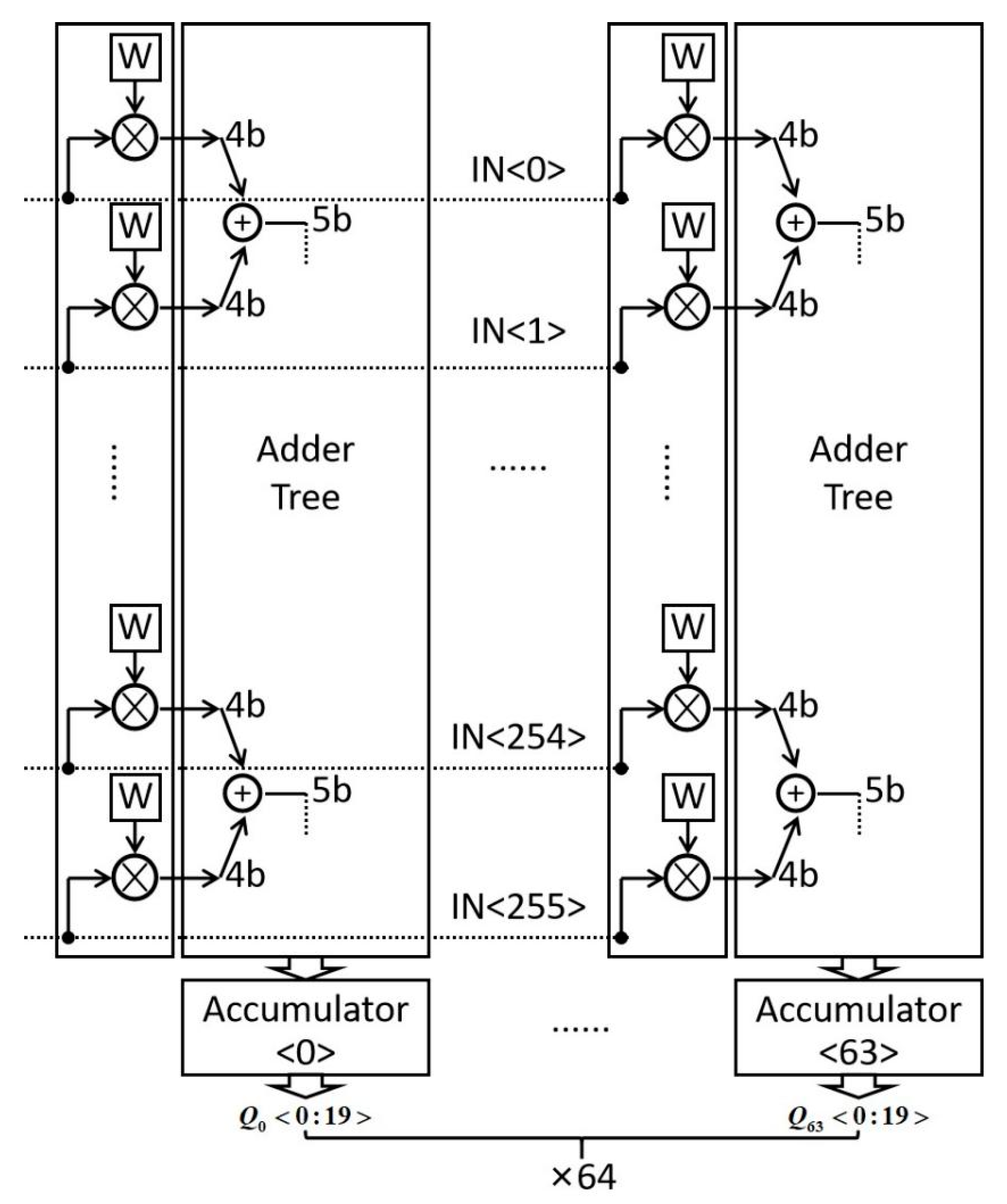
2.1. Digital CIM Macro

The digital CIM macro is typically constituted by a memory array, a parallel adder tree, and a partial-sum accumulator, as shown in Figure 1. The memory array contains memory units and logic operation gates. The parallel adder tree is a full-adder array that aims to add several narrow bit-width numbers to obtain a wider bit-width number. The partial-sum accumulator contains a shifter and a full adder. Taking the multiplication of unsigned 64 × 64 × 4b weights and 64 × 4b input activations as an example, the operation of the digital CIM macro will be introduced and detailed as follows. This macro contains 64 columns of sub-CIM units; each unit consists of a memory array that contains 64 × 4b weights and 64 × 4 bit-wise multipliers, a 6-stage parallel adder tree, and a partial-sum accumulator. In CIM operation, 64 × 4b input activations are simultaneously fed into the memory array in a bit-serial manner. The memory array performs 64 multiplications of 1b input activation and 4b weight in one computation cycle, while the results of multiplications are fed into the 6-stage parallel adder tree to generate a 10b partial sum. A partial-sum accumulator is required to accumulate the partial sums of each computation cycle, after the above four computation cycles, the partial-sum accumulator shifts and adds four 10b results to get a 14b result. Therefore, an extra computation cycle is required to output the accumulated result, and a total of 5 computation cycles are required to complete the MVM for input activations with 4b precision [24].

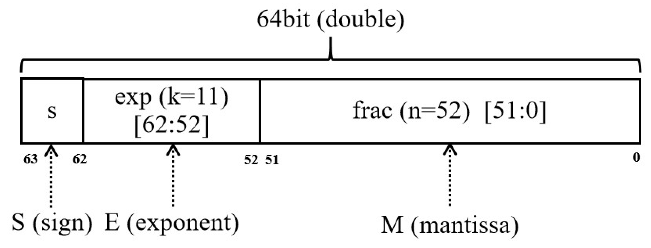
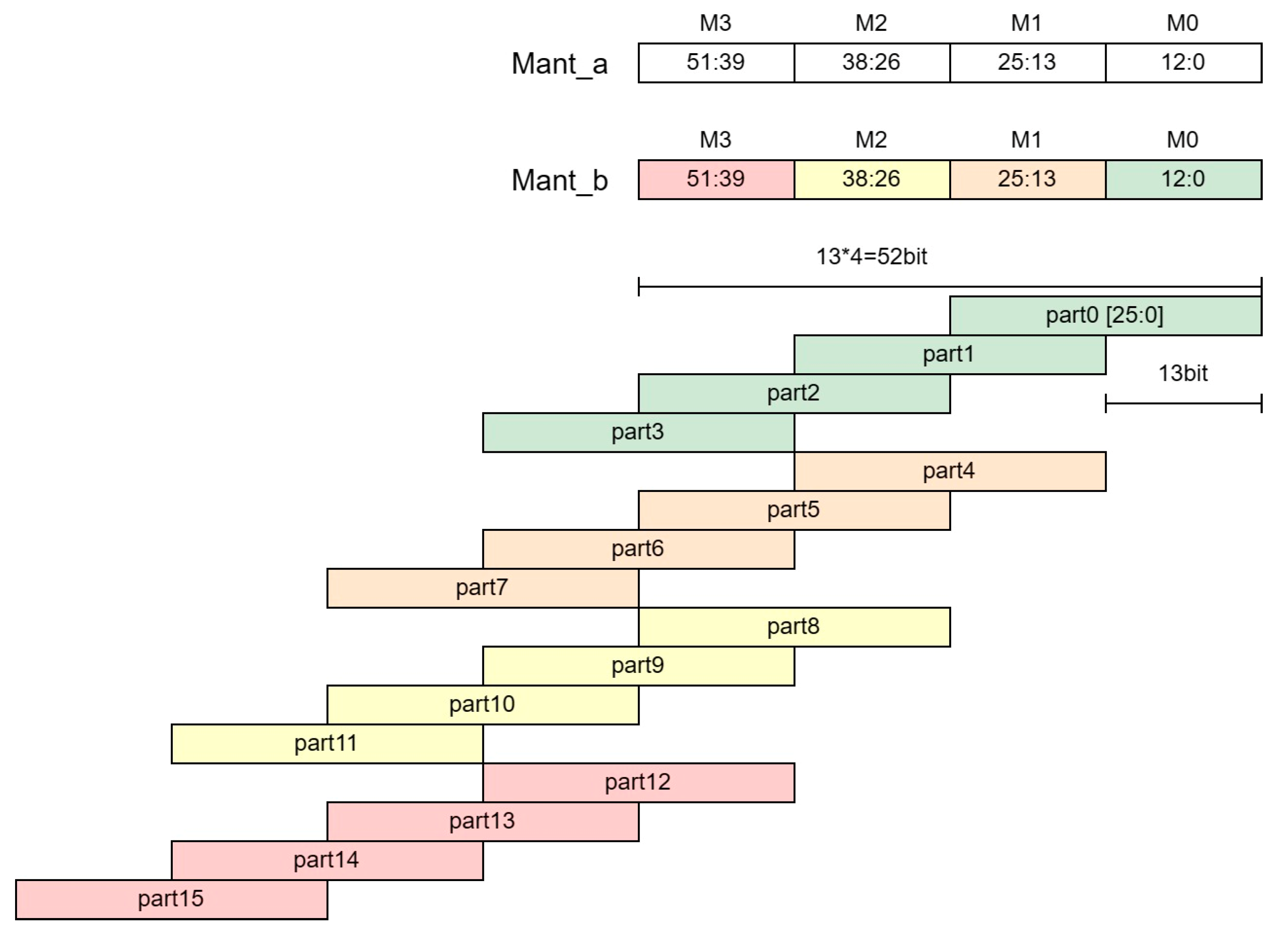
2.2. FP64 Data Format

According to the definition of IEEE binary floating-point arithmetic standard (IEEE 754), FP64 represents a data format that uses 8 bytes, in total, for encoding and storage. The storage space of FP64 is divided into three parts, as shown in Figure 2. The highest bit that expresses sign is abbreviated to S. The middle 11 bits, which express exponent, are abbreviated as E, while the lowest 52 bits, which express fraction, are abbreviated as M. The actual value of a normalized FP64 number N can be expressed as follows:
N = (−1)S × 2E−1023 × (1 × M)
The actual exponent value is equal to the difference between E represented in floating-point format and an exponential bias. With this representation, all exponent values can be represented by unsigned integers, which makes it easier to compare the exponent sizes of two floating-point numbers. If the value of the exponential part in FP64 is between 0 and 211–2, the most significant bit (integer bit) of the fractional part is 1, and N will be called normalized number. If the value of the exponential part in FP64 is 0 and the fractional part is non-zero, N will be called denormalized number. Generally, the denormalized number is used to represent numbers that are quite close to zero. IEEE 754 stipulates that the exponential bias of denormalized floating-point numbers is 1 less than that of normalized floating-point numbers [25,26].

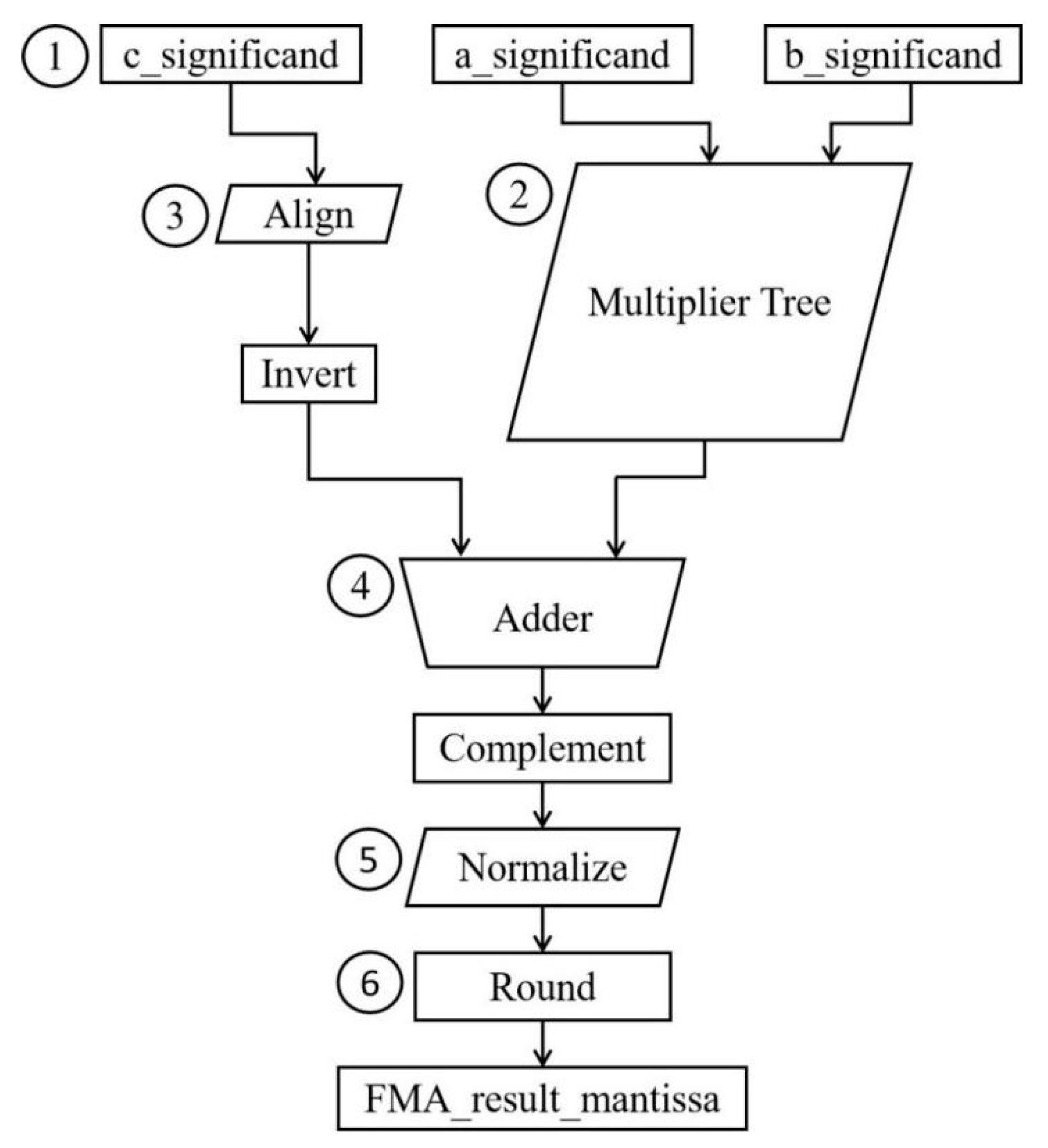
2.3. The Algorithm of FMA Operator

The operation a × b + c is often required in engineering applications and completed in two steps with two rounding operations. The FMA operator is introduced for the single instruction execution of this operation with single- or double-precision floating-point operands. This operator is designed to reduce the latency and provide greater floating-point arithmetic precision since only a single rounding operation is performed with an FMA operator on the combined full-precision product and sum.
The algorithm process of the FMA operator is shown in Figure 3. There are six serial steps to complete the execution of a FMA operation on traditional architecture [27,28,29]:
① Obtain the significands of a, b, and c, that is, add the integer bit and mantissa to obtain the significand.
② Add the exponents and multiply the significands of input a and b to complete the operation a × b.
③ Align the exponents of a × b and c, that is, shift the significands of the number with the smaller exponent to the right to increase the exponent until it equals the exponent of another number.
④ Add the significands of a × b and c.
⑤ Normalize the result, that is, shift the significand of the result to the left to reduce the exponent until the most significand bit is 1.
⑥ Round the result; due to the length of the result exceeding that of the data stored by the physical device in the computer, the lower bits need to be rounded to ensure that the result can be stored in the computer with relative accuracy, and the common method is to round to the nearest even number.

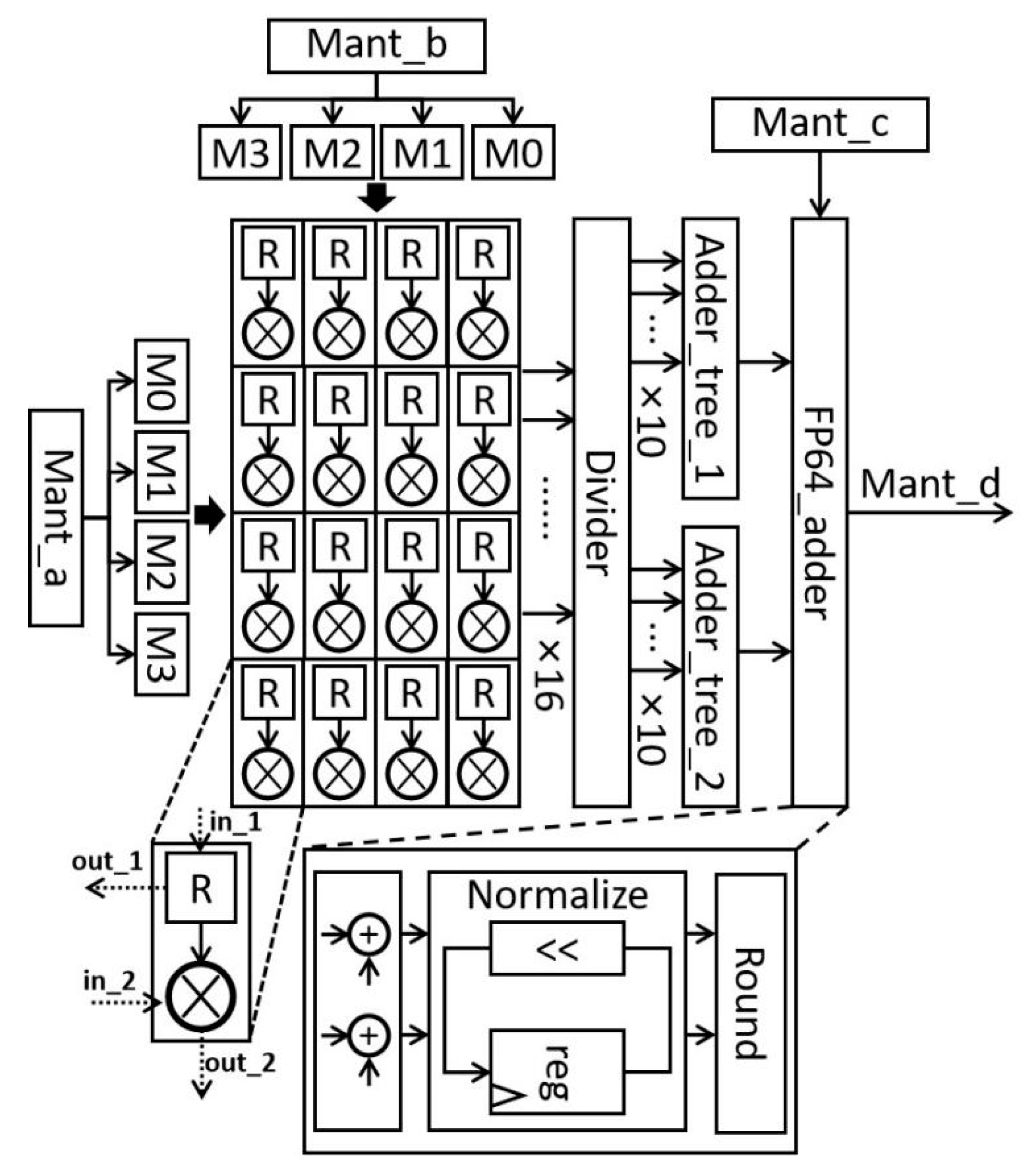
3. The Proposed Architecture of DCIM-FF

As shown in Figure 4, the DCIM-FF macro contains a 16 × 13b memory array, a divider module, two parallel adder trees (adder_tree_1 and adder_tree_2) and a FP64 adder module. The mantissas of inputs (a, b, and c) are represented by Mant_a, Mant_b, and Mant_c, and the mantissa of output (d) is represented by Mant_d. R represents the 13b register, while operands a, b, c, and d meet the equation:
a × b + c = d
FMA is the single-instruction execution of the formula a × b + c. In order to map the FP64-based FMA algorithm to the digital CIM circuit, some improvements were made to this algorithm, that is, splitting the operation of a × b into 16 multiplications and 15 additions, as shown in Figure 5; part0~part16 represent the 16 multiplication results from memory array. The 52b mantissas of inputs (a and b) are split into 13b in four parts: M0, M1, M2, and M3, respectively. A multiplication of 4 × 4 = 16 times is required due to the multiplication of 4 split mantissa parts of input a and b. As each split mantissa part is used 4 times in the 16 multiplications, each part is stored twice in a sub-CIM cell that is composed of a 13b register and a digital multiplier and is transmitted twice in the memory array, which contains 16 sub-CIM cells, to complete the 16 multiplications. Each sub-CIM cell obtains the split mantissa part as the multiplier from input a/b through the in_1 port connecting the 13b register and obtains the split mantissa part as the multiplicand from the other sub-CIM cell through the input_2 port connecting the digital multiplier. This cell outputs the split mantissa part from the 13b register to the other sub-CIM cells through the out_1 port and outputs part0~part16 to the divider module through out_2 port. In order to make the 16 outputs of the memory array meet the bit-width requirements of adder trees for input data, a divider module is placed to split 16 groups of data into 20 groups, which transforms the original required 15 additions into 18 additions.
Moreover, an n × 13b left shift is required for part0~part16 before being split in the divider module, as shown in Figure 5; a 13b left shift is required for part1; a 26b left shift is required for part2; a 39b left shift is required for part3; a 13b left shift is required for part4; a 26b left shift is required for part5; a 39b left shift is required for part6; a 52b left shift is required for part7; a 26b left shift is required for part8; a 39b left shift is required for part9; 52b left shift is required for part10; a 65b left shift is required for part11; a 39b left shift is required for part12; a 52b left shift is required for part13; a 65b left shift is required for part14; and a 78b left shift is required for part15. These shifted data will become partial products. The bit-width of the longest partial product reaches 104, and large bit-width adders will be required in the adder tree if these partial products are summed directly, which consumes a lot of area. Instead, we divide each partial product into two segments (high 52b and low 52b) from the middle line, and the actual bit-width of each segment will be no more than 52. In that way, the smaller area adders are adopted to combine these partial products, and two adder trees are required to add the two sets of partial products that come from high bits and low bits, respectively. The results of that divider module are fed into two parallel adder trees, which perform those 18 additions above. Each adder tree adopts a 4-stage pipelined structure to add 10 small bit-width data into a large bit-width partial mantissa in 4 computation cycles. The mantissa of a × b consists of the highest 56 bits and lowest 52 bits from those two adder trees, respectively. The mantissas of a × b and c are fed into the FP64 adder module to complete the addition of a × b and c. As described in the FMA algorithm, these steps will be performed in the FP64 adder module: the alignment of the exponents of a × b and c, the addition of the mantissas of a × b and d, normalization, and rounding. In contrast to the normalization model, the most significand bit of the result can be 0 in that model of DCIM-FF to support possible denormalized results. Once the exponent of the result is less than the minimum exponent value that FP64 can represent, the shifting of the significand in the result will stop and DCIM-FF will output a denormalized floating-point result.

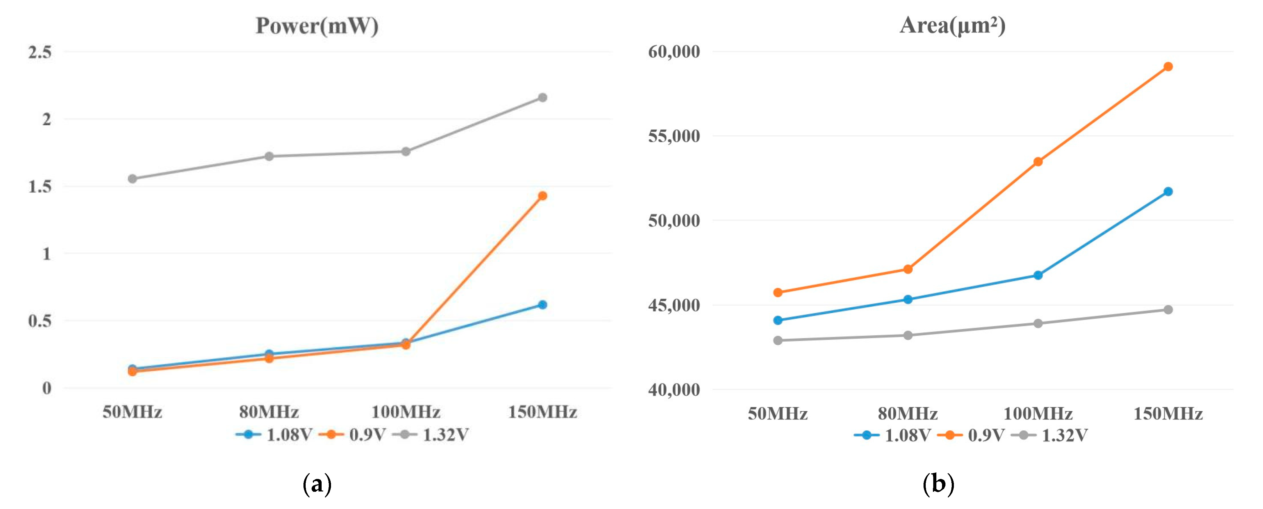
4. Simulation and Discussion

The model of the proposed DCIM-FF macro was implemented using Verilog. Simulations with extensive testing data were performed to verify the functionality of the proposed design. DCIM-FF was tested by the testbench, which produces a large number of random FP64s as incentives, and the corresponding codes were tested by a hardware description language (HDL) compiled simulation tool, where we verify the functionality of DCIM-FF by observing the waveform of each signal over time. We have verified that the DCIM-FF macro can provide the correct rounded implementations for normalized/denormalized inputs in round-to-nearest-even mode and round-to-zero mode, respectively. In order to show the accuracy of the DCIM-FF operating FMA, several complicated FP64 numbers were adopted as inputs to verify the correctness of the results. The srand and rand functions of the C99 stdlib library and the time function of C99 time library were used to generate the random FP64. In order to make the number of random FP64s reach millions in magnitude, the malloc function of the C99 stdlib library was used to allocate a specified amount of memory space for a large number of random data in the heap area. The FMA function in the C99 math library was used as the standard reference during the verification process. In addition, the model of DCIM-FF was built using C language at software level, which runs faster than the HDL-based hardware model. The C model will also be taken as a comparative reference for the simulation results of DCIM-FF at hardware level. Two million sets of complicated FP64 input data were tested through the random-number-testing device, and the results were consistent with the standard reference. As shown in Table 1, the 4 representative sets of tested results were extracted for display; we use hexadecimal numbers starting with 0x to represent 64b operands. At the set of normalized numbers, a is 0x405676f4ede9dbd4, which is approximately 89.8586993011 in decimal representation; b is 0x40340aa015402a80, which is approximately 20.0415051729 in decimal representation; c is 0x407726f04de09bc1, which is approximately 370.4336680197 in decimal representation; and d is 0x40a0f6acacac57ff, which is approximately 2171.337254892 in decimal representation. At the set of denormalized numbers, a is 0xac7e15859290f, which is approximately 1.4992522965 × 10−308 (scientific notation) in decimal representation; the value of the exponential part in FP64 is 0 for number a, which is quite close to zero; b is 0x3fdf9fbf3f7e7efd, which is approximately 0.4941251869 in decimal representation; the value of the exponential part in FP64 is non-zero for number b; c is 0xd375c9a74d3d, which is approximately 1.1487166967 × 10−309 (scientific notation) in decimal representation; the value of the exponential part in FP64 is 0 for number c, which is quite close to zero; d is 0x6272fbb808f07, which is approximately 8.5568999093 × 10−309 (scientific notation) in decimal representation; the value of the exponential part in FP64 is 0 for number d, which is quite close to zero. Equation (2) can be verified from decimal arithmetic.
The guard bit, round bit, and sticky bit are used to determine whether to carry when removing some trailing bits from the binary number. The guard bit is the least significant of the valuable bits. The first two of the bits to be removed are the round bit and sticky bit, respectively. The remaining bits are the bits to be removed except for the round bit. In round-to-zero mode, the available bits are kept and the rest are thrown away, which has the effect of making the value represented closer to 0.0. Compared with round-up mode, round-to-nearest-even mode works differently when the calculated value is exactly half- way between the two possible final results. For example, in round-to-nearest-even mode, the action depends on the relationship of the remaining bits to zero if the round bit equals 1. If the remaining bits are greater than zero, then the calculated values need to be increased. If the remaining bits are equal to zero, the calculated values will be rounded to the closest even number, specifically, the calculated values need to be increased when the sticky bit is equal to 1. Moreover, the calculated value will be truncated to obtain the final result if the round bit is equal to 0 in both round-to-nearest-even mode and round-to-zero mode. To verify the rounding functionality of DCIM-FF, we use the same set of input data in both round-to-nearest-even mode and round-to-zero mode. At the set of input data in the two rounding modes, a is 0x404a084410882110, which is approximately 52.0645771661 in decimal representation; b is 0xc0510df41be837d0, which is approximately −68.2180242317 in decimal representation; the value of the sign bit in FP64 is 1 for number b, which is a negative number; c is 0xc08603ab87570eae, which is approximately −704.4587542344 in decimal representation; the value of the sign bit in FP64 is 1 for number c, which is negative number. For the mantissa calculated result using the above input data, the guard bit is 0; the round bit is 1; and the remaining bits are greater than zero. According to the above theory, the calculated value needs to be increased in round-to-nearest-even mode and truncated in round-to-zero mode. At the set of output data, d is equal to 0xc0b0a0338b14cb85 in round-to-nearest-even mode and 0xc0b0a0338b14cb84 in round-to-zero mode, which are both approximately −4256.2013409612 in decimal representation; the value of the sign bit in FP64 is 1 for number d, which is a negative number. The results from those two modes shows a 1-bit difference from each other due to different rounding methods, which is consistent with the theory above. Due to the huge amount of data tested in the simulation (2 million groups), it is difficult to show all of them in this article, and only some samples can be used for display. More sampled test results can be found in Table 2, where the numbers in parentheses indicate approximately the decimal value corresponding to the 64b operand. Equation (2) (a × b + c = d) can be verified from decimal arithmetic.
The DCIM-FF was synthesized with CMOS-55 nm technology with normal case parameters using related software. As shown in Figure 6, it dissipates 0.12–2.16 mW at 50–150 MHz operating frequency with 0.9–1.32 V supply voltage. The power efficiency of DCIM-FF can reach up to 26.9 TOPS/W. Compared to previous FMA designs, the proposed DCIM-FF macro achieves FMA functionality with significant power efficiency improvement and less area overhead, based on CIM technology. The comparison of DCIM-FF with some other FMA works that support FP64 arithmetic is shown in Table 3 [30,31,32,33,34]. DCIM-FF completes a FMA operation for a total of nine computation cycles, which causes a delay of 60 ns at 150 MHz operating frequency. There are four computation cycles of DCIM-FF consumed in the pipeline architecture of adder trees and five computation cycles consumed in the normalization operation of the FP64_adder module. The throughput of DCIM-FF can be obtained by calculating the reciprocal of the delay, which is approximately 16.7 MOPS and represents the number of operations that can be completed by the macro per second. As can be seen from Table 3, the comprehensive performance of the proposed design in [33] is optimal among all references. Ref. [33] presented a three-stage, eight-level, pipelined, dual-precision FMA design that can perform operations either at one double-precision or at two single-precisions in parallel. In terms of area and power consumption, DCIM-FF takes over 65% less area and improves power efficiency by more than 50% compared to the previous FMA design in [33].

5. Conclusions

This paper presents a novel all-digital CIM macro-DCIM-FF to complete FP64-based fused multiply-add (FMA) operations for the first time, which can provide correct rounded implementations for normalized/denormalized inputs in round-to-nearest-even mode and round-to-zero mode, respectively. We have verified the functionality of DCIM-FF through pre-production simulation, and we have synthesized the DCIM-FF macro with a 55 nm technology development kit. The power efficiency of DCIM-FF can reach up to 26.9 TOPS/W with 0.12–2.16 mW at 50–150 MHz operating frequency. Circuit-level simulation results show that DCIM-FF achieves significant power efficiency improvement and less area overhead compared with previous FMA designs. This work completes FP64 arithmetic based on the digital CIM technology and proposes a novel architecture for accelerating FMA operation, which exhibits approximately a 15-fold increase in power efficiency compared with the previous FMA design (1.64 TOPS/W) [35]. While DCIM-FF is insufficient in terms of throughput, in future work, we can reduce the computation cycles of DCIM in the normalization operation and adopt the pipeline architecture in the adder trees for other long-stage logical operation modules to achieve a higher operating frequency and throughput. Moreover, DCIM-FF paves a novel pathway for subsequent implementation of FP64-based MVM operation by CIM. DCIM-FF can be used as a MVM computing unit, since MVM is essentially a repeated multiply-add operation. The use of CIM to achieve FP64-based MVM operation will be conducive to the application of CIM technology for hyperscale scientific computing.

Author Contributions

Conceptualization, D.L., K.M. and B.P.; methodology, K.M. and B.P.; software, K.M.; validation, D.L. and K.M.; formal analysis, K.M.; investigation, K.M.; resources, B.P. and W.L.; data curation, K.M. and L.L. (Lei Li); writing—original draft, K.M., L.L. (Liang Liu) and B.P.; writing—review and editing, K.M., L.L. (Liang Liu), B.P. and L.L. (Lei Li); visualization, K.M. and W.L.; supervision, B.P. and W.K.; project administration, B.P.; funding acquisition, B.P. All authors have read and agreed to the published version of the manuscript.

Funding

This research was supported partly by The Laboratory Open Fund of Beijing Smart-Chip Microelectronics Technology Co., Ltd., and partly by the National Natural Science Foundation of China (62001019).

Data Availability Statement

We currently have no data supporting results.

Conflicts of Interest

The authors declare no conflict of interest.

References

  1. Tan, L.; Kothapalli, S.; Chen, L.; Hussaini, O.; Bissiri, R.; Chen, Z. A survey of power and energy efficient techniques for high performance numerical linear algebra operations. Parallel Comput. 2014, 40, 559–573. [Google Scholar] [CrossRef]
  2. Chen, J.; Li, J.; Li, Y.; Miao, X. Multiply accumulate operations in memristor crossbar arrays for analog computing. J. Semicond. 2021, 42, 013104. [Google Scholar] [CrossRef]
  3. Feinberg, B.; Vengalam UK, R.; Whitehair, N.; Wang, S.; Ipek, E. Enabling scientific computing on memristive accelerators. In Proceedings of the 2018 ACM/IEEE 45th Annual International Symposium on Computer Architecture (ISCA), Los Angeles, CA, USA, 1–6 June 2018. [Google Scholar]
  4. Kautz, W.H. Cellular logic-in-memory arrays. IEEE Trans. Comput. 1969, 100, 719–727. [Google Scholar] [CrossRef]
  5. Stone, H.S. A logic-in-memory computer. IEEE Trans. Comput. 1970, 100, 73–78. [Google Scholar] [CrossRef]
  6. Ahn, J.; Yoo, S.; Mutlu, O.; Choi, K. PIM-enabled instructions: A low-overhead, locality-aware processing-in-memory architecture. ACM SIGARCH Comput. Archit. News 2015, 43, 336–348. [Google Scholar] [CrossRef]
  7. Elliott, D.G.; Stumm, M.; Snelgrove, W.M.; Cojocaru, C.; McKenzie, R. Computational RAM: Implementing processors in memory. IEEE Des. Test Comput. 1999, 16, 32–41. [Google Scholar] [CrossRef]
  8. Li, S.; Niu, D.; Malladi, K.T.; Zheng, H.; Brennan, B.; Xie, Y. Drisa: A dram-based reconfigurable in-situ accelerator. In Proceedings of the 2017 50th Annual IEEE/ACM International Symposium on Microarchitecture (MICRO), Cambridge, MA, USA, 14–18 October 2017. [Google Scholar]
  9. Wong HS, P.; Salahuddin, S. Memory leads the way to better computing. Nat. Nanotechnol. 2015, 10, 191–194. [Google Scholar] [CrossRef] [PubMed] [Green Version]
  10. Heo, J.; Kim, J.; Lim, S.; Han, W.; Kim, J.Y. T-PIM: An Energy-Efficient Processing-in-Memory Accelerator for End-to-End On-Device Training. IEEE J. Solid-State Circuits 2022, 58, 600–613. [Google Scholar] [CrossRef]
  11. Dong, Q.; Sinangil, M.E.; Erbagci, B.; Sun, D.; Khwa, W.S.; Liao, H.J.; Wang, Y.; Chang, J. 15.3 A 351TOPS/W and 372.4 GOPS compute-in-memory SRAM macro in 7nm FinFET CMOS for machine-learning applications. In Proceedings of the 2020 IEEE International Solid-State Circuits Conference-(ISSCC), San Francisco, CA, USA, 16–20 February 2020. [Google Scholar]
  12. Zhao, C.; Fang, J.; Jiang, J.; Xue, X.; Zeng, X. ARBiS: A Hardware-Efficient SRAM CIM CNN Accelerator With Cyclic-Shift Weight Duplication and Parasitic-Capacitance Charge Sharing for AI Edge Application. IEEE Trans. Circuits Syst. I Regul. Pap. 2022, 70, 364–377. [Google Scholar] [CrossRef]
  13. Seshadri, V.; Lee, D.; Mullins, T.; Hassan, H.; Boroumand, A.; Kim, J.; Mowry, T.C. Ambit: In-memory accelerator for bulk bitwise operations using commodity DRAM technology. In Proceedings of the 2017 50th Annual IEEE/ACM International Symposium on Microarchitecture (MICRO), Cambridge, MA, USA, 14–18 October 2017. [Google Scholar]
  14. Sebastian, A.; Le Gallo, M.; Khaddam-Aljameh, R.; Eleftheriou, E. Memory devices and applications for in-memory computing. Nat. Nanotechnol. 2020, 15, 529–544. [Google Scholar] [CrossRef] [PubMed]
  15. Li, S.; Xu, C.; Zou, Q.; Zhao, J.; Lu, Y.; Xie, Y. Pinatubo: A processing-in-memory architecture for bulk bitwise operations in emerging non-volatile memories. In Proceedings of the 53rd Annual Design Automation Conference, Austin, TX, USA, 5–9 June 2016. [Google Scholar]
  16. Si, X.; Tu, Y.N.; Huang, W.H.; Su, J.W.; Lu, P.J.; Wang, J.H.; Liu, T.W.; Wu, S.Y.; Liu, R.; Chou, Y.C.; et al. 15.5 A 28nm 64Kb 6T SRAM computing-in-memory macro with 8b MAC operation for AI edge chips. In Proceedings of the 2020 IEEE International Solid-State Circuits Conference-(ISSCC), San Francisco, CA, USA, 16–20 February 2020. [Google Scholar]
  17. Su, J.W.; Si, X.; Chou, Y.C.; Chang, T.W.; Huang, W.H.; Tu, Y.N.; Liu, R.; Lu, P.J.; Liu, T.W.; Wang, J.H.; et al. 15.2 a 28nm 64Kb inference-training two-way transpose multibit 6T SRAM Compute-in-Memory macro for AI edge chips. In Proceedings of the 2020 IEEE International Solid-State Circuits Conference-(ISSCC), San Francisco, CA, USA, 16–20 February 2020. [Google Scholar]
  18. Su, J.W.; Chou, Y.C.; Liu, R.; Liu, T.W.; Lu, P.J.; Wu, P.C.; Chung, Y.L.; Hung, L.Y.; Ren, J.S.; Pan, T.; et al. 16.3 a 28nm 384kb 6t-sram computation-in-memory macro with 8b precision for ai edge chips. In Proceedings of the 2021 IEEE International Solid-State Circuits Conference (ISSCC), San Francisco, CA, USA, 13–22 February 2021; Volume 64. [Google Scholar]
  19. Yue, J.; Yuan, Z.; Feng, X.; He, Y.; Zhang, Z.; Si, X.; Liu, R.; Chang, M.F.; Li, X.; Yang, H.; et al. 14.3 a 65nm computing-in-memory-based cnn processor with 2.9-to-35.8 tops/w system energy efficiency using dynamic-sparsity performance-scaling architecture and energy-efficient inter/intra-macro data reuse. In Proceedings of the 2020 IEEE International Solid-State Circuits Conference-(ISSCC), San Francisco, CA, USA, 16–20 February 2020. [Google Scholar]
  20. Eckert, C.; Wang, X.; Wang, J.; Subramaniyan, A.; Iyer, R.; Sylvester, D.; Blaaauw, D.; Das, R. Neural cache: Bit-serial in-cache acceleration of deep neural networks. In Proceedings of the 2018 ACM/IEEE 45Th Annual International Symposium on Computer Architecture (ISCA), Los Angeles, CA, USA, 1–6 June 2018. [Google Scholar]
  21. Yue, J.; Feng, X.; He, Y.; Huang, Y.; Wang, Y.; Yuan, Z.; Zhan, M.; Liu, J.; Su, J.W.; Chung, Y.L.; et al. 15.2 A 2.75-to-75.9 TOPS/W computing-in-memory NN processor supporting set-associate block-wise zero skipping and ping-pong CIM with simultaneous computation and weight updating. In Proceedings of the 2021 IEEE International Solid-State Circuits Conference (ISSCC), San Francisco, CA, USA, 13–22 February 2021; Volume 64. [Google Scholar]
  22. Fujiwara, H.; Mori, H.; Zhao, W.C.; Chuang, M.C.; Naous, R.; Chuang, C.K.; Hashizume, T.; Sun, D.; Lee, C.F.; Akarvardar, K.; et al. A 5-nm 254-TOPS/W 221-TOPS/mm 2 Fully-Digital Computing-in-Memory Macro Supporting Wide-Range Dynamic-Voltage-Frequency Scaling and Simultaneous MAC and Write Operations. In Proceedings of the 2022 IEEE International Solid-State Circuits Conference (ISSCC), San Francisco, CA, USA, 20–26 February 2022; Volume 65. [Google Scholar]
  23. Tu, F.; Wang, Y.; Wu, Z.; Liang, L.; Ding, Y.; Kim, B.; Liu, L.; Wei, S.; Xie, Y.; Yin, S. A 28nm 29.2 TFLOPS/W BF16 and 36.5 TOPS/W INT8 Reconfigurable Digital CIM Processor with Unified FP/INT Pipeline and Bitwise In-Memory Booth Multiplication for Cloud Deep Learning Acceleration. In Proceedings of the 2022 IEEE International Solid-State Circuits Conference (ISSCC), San Francisco, CA, USA, 20–26 February 2022; Volume 65. [Google Scholar]
  24. Chih, Y.D.; Lee, P.H.; Fujiwara, H.; Shih, Y.C.; Lee, C.F.; Naous, R.; Chen, Y.L.; Lo, C.P.; Lu, C.H.; Mori, H.; et al. 16.4 an 89tops/w and 16.3 tops/mm 2 all-digital sram-based full-precision compute-in memory macro in 22nm for machine-learning edge applications. In Proceedings of the 2021 IEEE International Solid-State Circuits Conference (ISSCC), San Francisco, CA, USA, 13–22 February 2021; Volume 64. [Google Scholar]
  25. Whitehead, N.; Fit-Florea, A. Precision & performance: Floating point and IEEE 754 compliance for NVIDIA GPUs. rn (A+ B) 2011, 21, 18749–19424. [Google Scholar]
  26. Szydzik, T.; Moloney, D. Precision refinement for media-processor SoCs: fp32-> fp64 on myriad. In Proceedings of the 2014 IEEE Hot Chips 26 Symposium (HCS), Las Palmas, Gran Canaria, Spain, 10–12 August 2014. [Google Scholar]
  27. Zhang, H.; Chen, D.; Ko, S.B. Efficient multiple-precision floating-point fused multiply-add with mixed-precision support. IEEE Trans. Comput. 2019, 68, 1035–1048. [Google Scholar] [CrossRef]
  28. Park, J.; Lee, S.; Jeon, D. A neural network training processor with 8-bit shared exponent bias floating point and multiple-way fused multiply-add trees. IEEE J. Solid-State Circuits 2021, 57, 965–977. [Google Scholar] [CrossRef]
  29. Stepchenkov, Y.; Stepchenkov, D.; Rogdestvenski, Y.; Shikunov, Y.; Diachenko, Y. Energy efficient speed-independent 64-bit fused multiply-add unit. In Proceedings of the 2019 IEEE Conference of Russian Young Researchers in Electrical and Electronic Engineering (EIConRus), Saint Petersburg and Moscow, Russia, 28–31 January 2019. [Google Scholar]
  30. Huang, L.; Shen, L.; Dai, K.; Wang, Z. A new architecture for multiple-precision floating-point multiply-add fused unit design. In Proceedings of the 18th IEEE Symposium on Computer Arithmetic (ARITH’07), Montpellier, France, 25–27 June 2007. [Google Scholar]
  31. Manolopoulos, K.; Reisis, D.; Chouliaras, V.A. An efficient dual-mode floating-point multiply-add fused unit. In Proceedings of the 2010 17th IEEE International Conference on Electronics, Circuits and Systems, Athens, Greece, 12–15 December 2010. [Google Scholar]
  32. Gök, M.; Özbilen, M.M. Multi-functional floating-point MAF designs with dot product support. Microelectron. J. 2008, 39, 30–43. [Google Scholar]
  33. Arunachalam, V.; Raj, A.N.J.; Hampannavar, N.; Bidul, C.B. Efficient dual-precision floating-point fused-multiply-add architecture. Microprocess. Microsyst. 2018, 57, 23–31. [Google Scholar]
  34. Quinnell, E.; Swartzlander, E.E.; Lemonds, C. Floating-point fused multiply-add architectures. In Proceedings of the 2007 Conference Record of the Forty-First Asilomar Conference on Signals, Systems and Computers, Pacific Grove, CA, USA, 4–7 November 2007. [Google Scholar]
  35. Hokenek, E.; Montoye, R.K.; Cook, P.W. Second-generation RISC floating point with multiply-add fused. IEEE J. Solid-State Circuits 1990, 25, 1207–1213. [Google Scholar] [CrossRef] [Green Version]
Figure 1. Illustration of the typical digital CIM design.
Applsci 13 04085 g001
Figure 2. The storage format of FP64 in computer.
Applsci 13 04085 g002
Figure 3. The algorithm diagram of FMA operator.
Applsci 13 04085 g003
Figure 4. Illustration of the DCIM-FF macro.
Applsci 13 04085 g004
Figure 5. The paradigm of the mantissa multiplication in DCIM-FF.
Applsci 13 04085 g005
Figure 6. Power consumption of DCIM-FF with various supply voltages (a). Area overhead of DCIM-FF with various supply voltage (b).
Applsci 13 04085 g006
Table 1. Sample 1 results of DCIM-FF.
Input/OutputData form
NormalizedDenormalized
Inputa0x405676f4ede9dbd40xac7e15859290f
b0x40340aa015402a800x3fdf9fbf3f7e7efd
c0x407726f04de09bc10xd375c9a74d3d
Outputd0x40a0f6acacac57ff0x6272fbb808f07
Input/OutputRounding mode
Round-to-Nearest-evenRound-to-Zero
Input a0x404a0844108821100x404a084410882110
b0xc0510df41be837d00xc0510df41be837d0
c0xc08603ab87570eae0xc08603ab87570eae
Outputd0xc0b0a0338b14cb850xc0b0a0338b14cb84
Table 2. Sample 2 results of DCIM-FF.
InputOutput
abcd
0x40485194a3294653
(48.64)
0x4043b7cf6f9edf3e
(39.44)
0x408c3336e66dccdc
(902.40)
0x40a608ee290e4081
(2820.47)
0x405676f4ede9dbd4
(89.86)
0x40340aa015402a80
(20.04)
0x407726f04de09bc1
(370.43)
0x40a0f6acacac57ff
(2171.34)
0x403d5982b305660b
(29.35)
0x4052a5f94bf297e5
(74.59)
0x4084a6c84d909b21
(660.85)
0x40a64445c82b8f97
(2850.14)
0x4053b5a96b52d6a6
(78.84)
0x403633c46788cf12
(22.20)
0x408507b58f6b1ed6
(672.96)
0x40a2eeb45c197595
(2423.35)
0x40580ec81d903b20
(96.23)
0x40585af4b5e96bd3
(97.42)
0x4077c61f8c3f187e
(380.38)
0x40c30da89eda44c6
(9755.32)
0x40224af495e92bd2
(9.15)
0x4056940f281e503d
(90.31)
0x408d1d98bb317663
(931.70)
0x409b76f7d9f00be1
(1757.74)
0x40182bb05760aec1
(6.04)
0x4051e68fcd1f9a3f
(71.60)
0x405128b6516ca2d9
(68.64)
0x407f54e634717e2c
(501.31)
0x4035cbdb97b72f6e
(21.80)
0x402e5dacbb5976b3
(15.18)
0x4085b413e827d050
(694.51)
0x409005c4f3053501
(1025.44)
0x4019d4b3a96752cf
(6.46)
0x404265e8cbd197a3
(36.80)
0x407edc24b8497093
(493.76)
0x4086db06849fa665
(731.38)
0x4050f2ffe5ffcc00
(67.80)
0x40574e329c6538ca
(93.22)
0x40882edcddb9bb73
(773.86)
0x40bbb601b2e4538b
(7094.01)
0x4055877f0efe1dfc
(86.12)
0x4058a97952f2a5e5
(98.65)
0x407146fc8df91bf2
(276.44)
0x40c121dc66dc7400
(8771.72)
0x40454d4a9a95352a
(42.60)
0x40425f44be897d13
(36.74)
0x408073cc6798cf32
(526.47)
0x40a057d8496a0647
(2091.92)
0x402b9cf739ee73dd
(13.81)
0x4045124e249c4939
(42.14)
0x4081a05840b08161
(564.04)
0x4091e7931bfbd1a3
(1145.89)
0x404ed729ae535ca7
(61.68)
0x402c429885310a62
(14.13)
0x40842ee7ddcfbb9f
(645.86)
0x4097b5ad8d59deb1
(1517.42)
0x3ffdeebbdd77baef
(1.87)
0x4042f095e12bc258
(37.88)
0x408d9f3d3e7a7cf5
(947.90)
0x408fd627ca73d130
(1018.77)
Table 3. Comparison of the proposed DCIM-FF with previous works.
FMA Designs Cycles Delay (ns) Area (μm2) Power (mW) Throughput (MOPS) Power Efficiency (TOPS/W)
[30]33.40708,590-294-
[31]33.34286,76635.22918.27
[32]43.611,803,624-277-
[33]83.24149,00017.830817.3
[34]11.08259,0054259262.18
This work96051,7030.6216.726.9
Disclaimer/Publisher’s Note: The statements, opinions and data contained in all publications are solely those of the individual author(s) and contributor(s) and not of MDPI and/or the editor(s). MDPI and/or the editor(s) disclaim responsibility for any injury to people or property resulting from any ideas, methods, instructions or products referred to in the content.

