
A New Control Scheme for the Buck Converter
 ,
, 
Abstract
:1. Introduction
2. Proposed Control Methodology
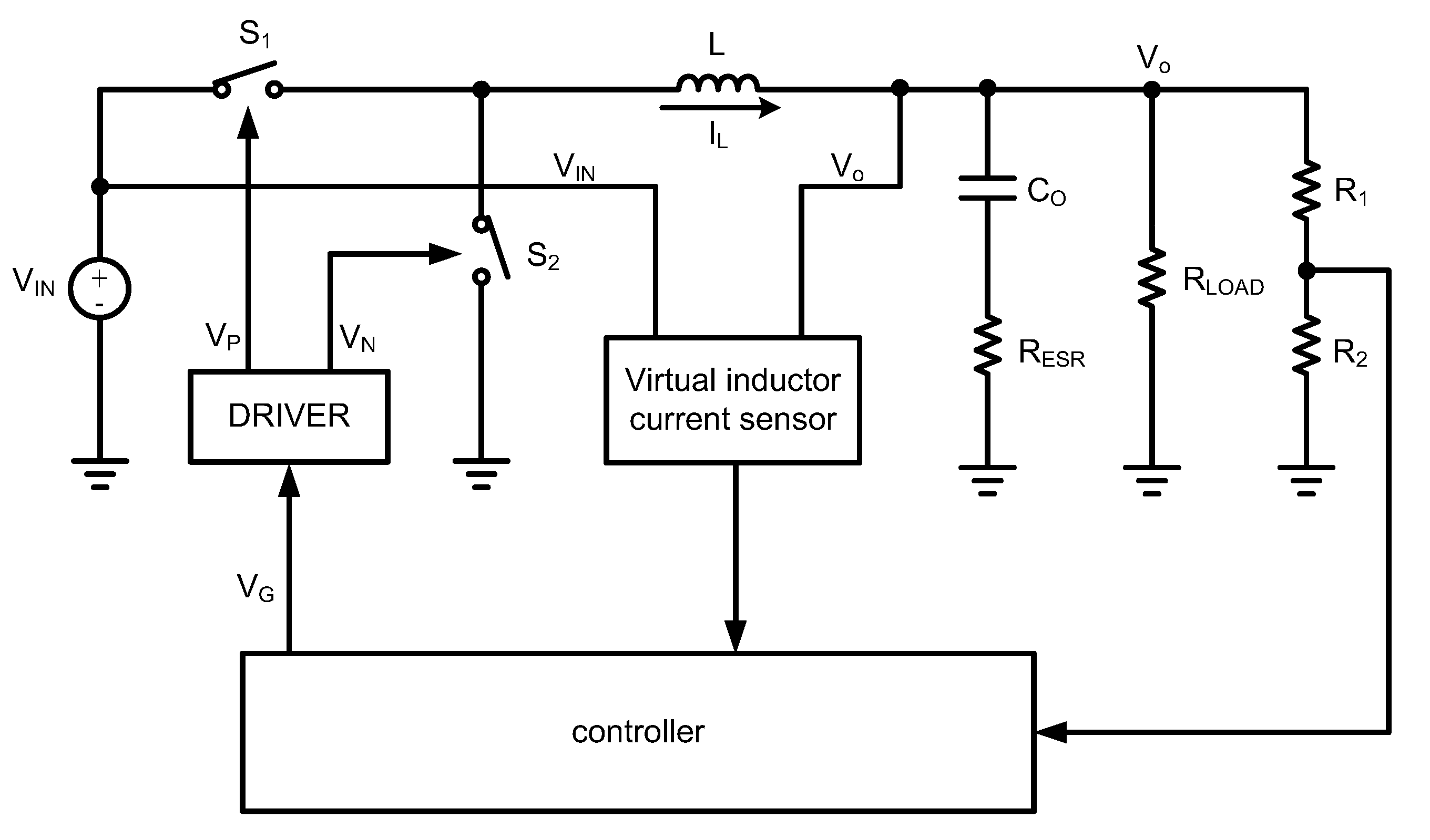
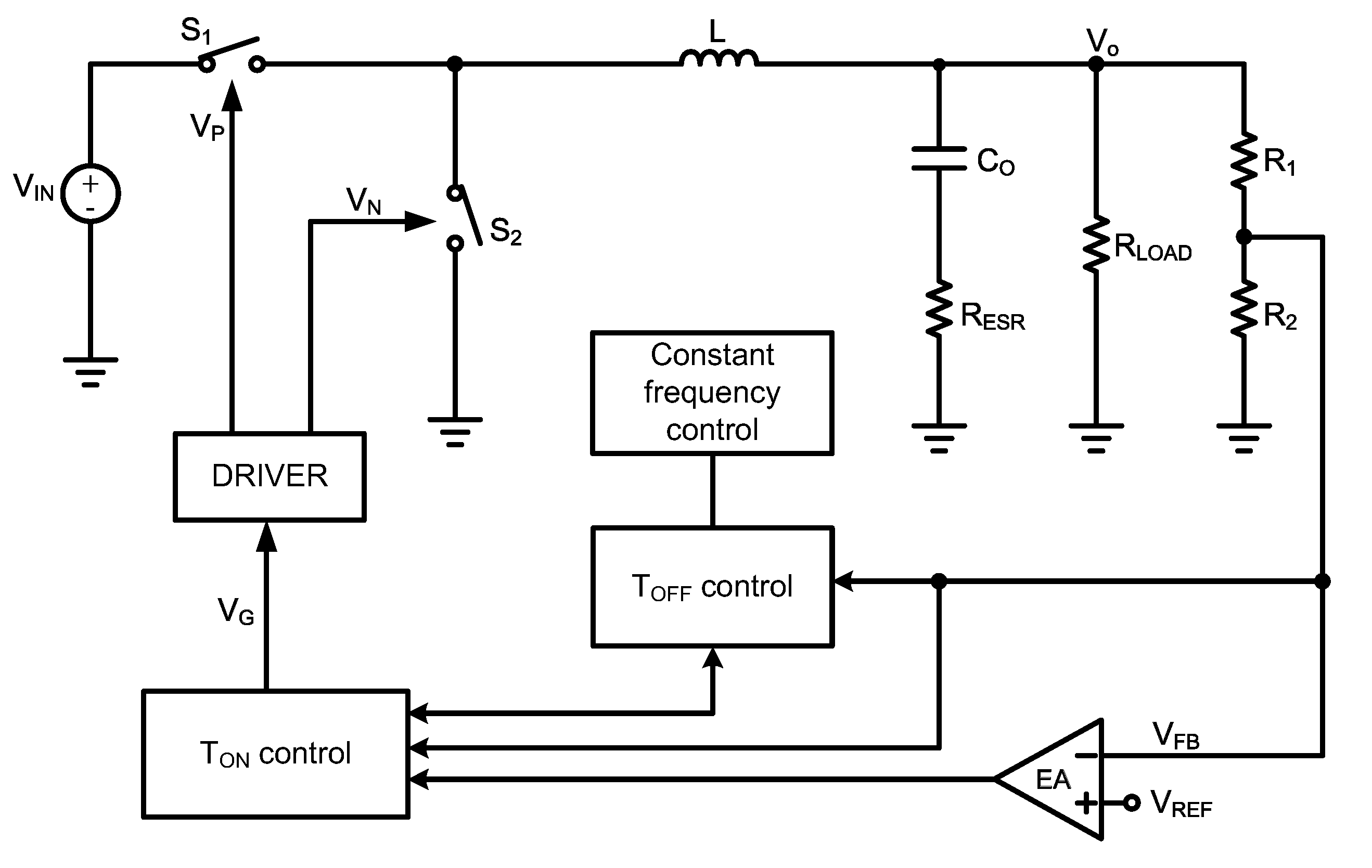
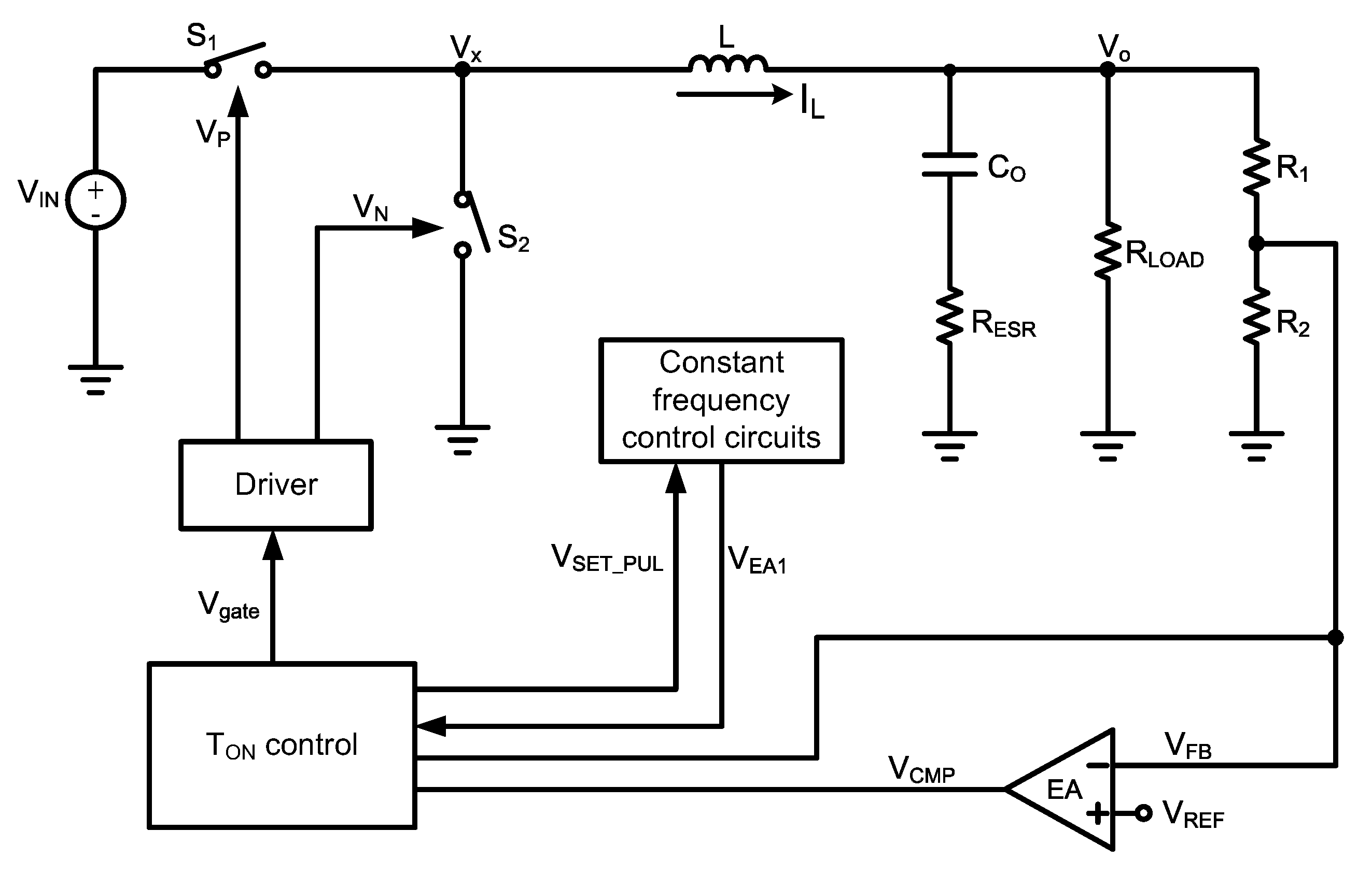
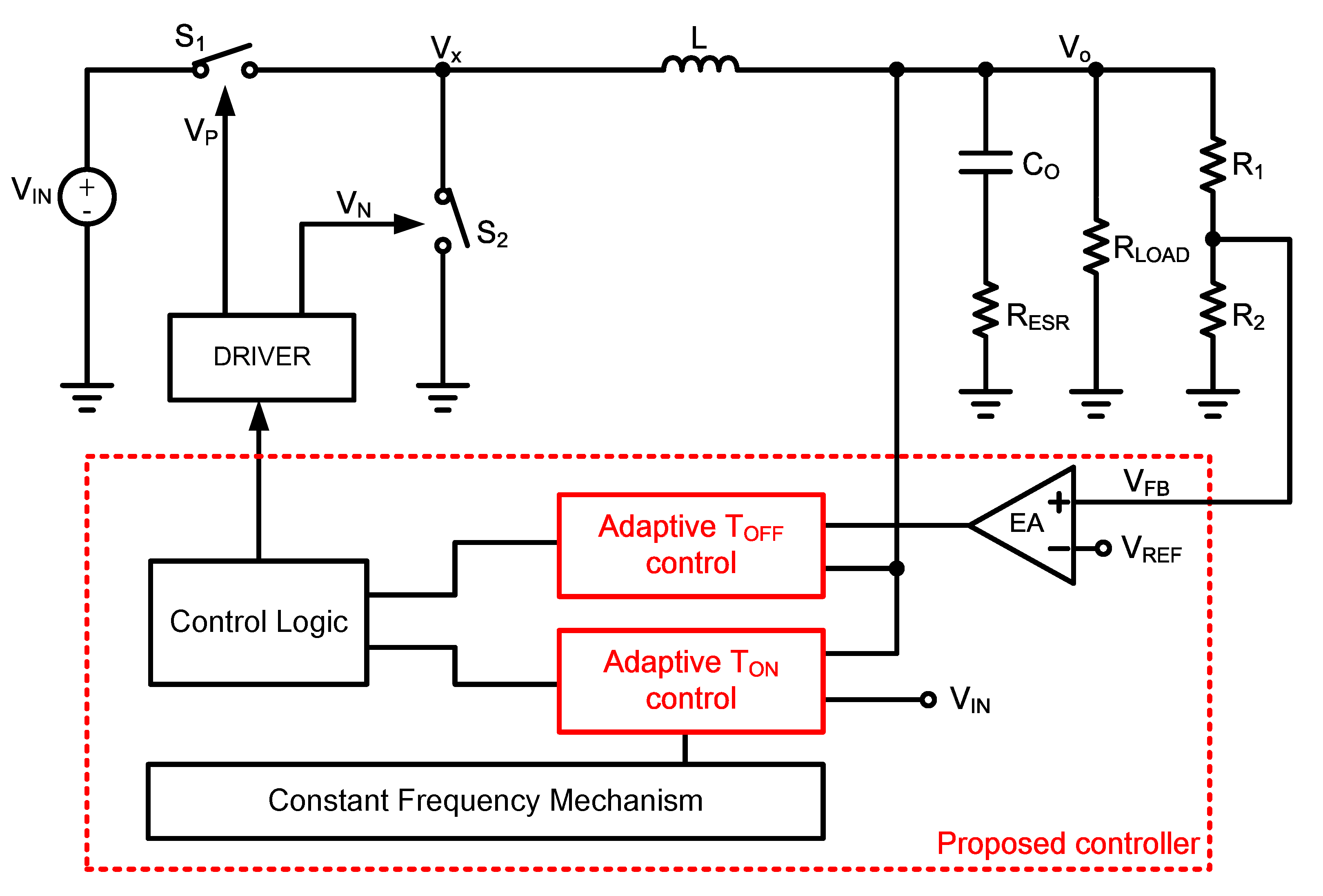
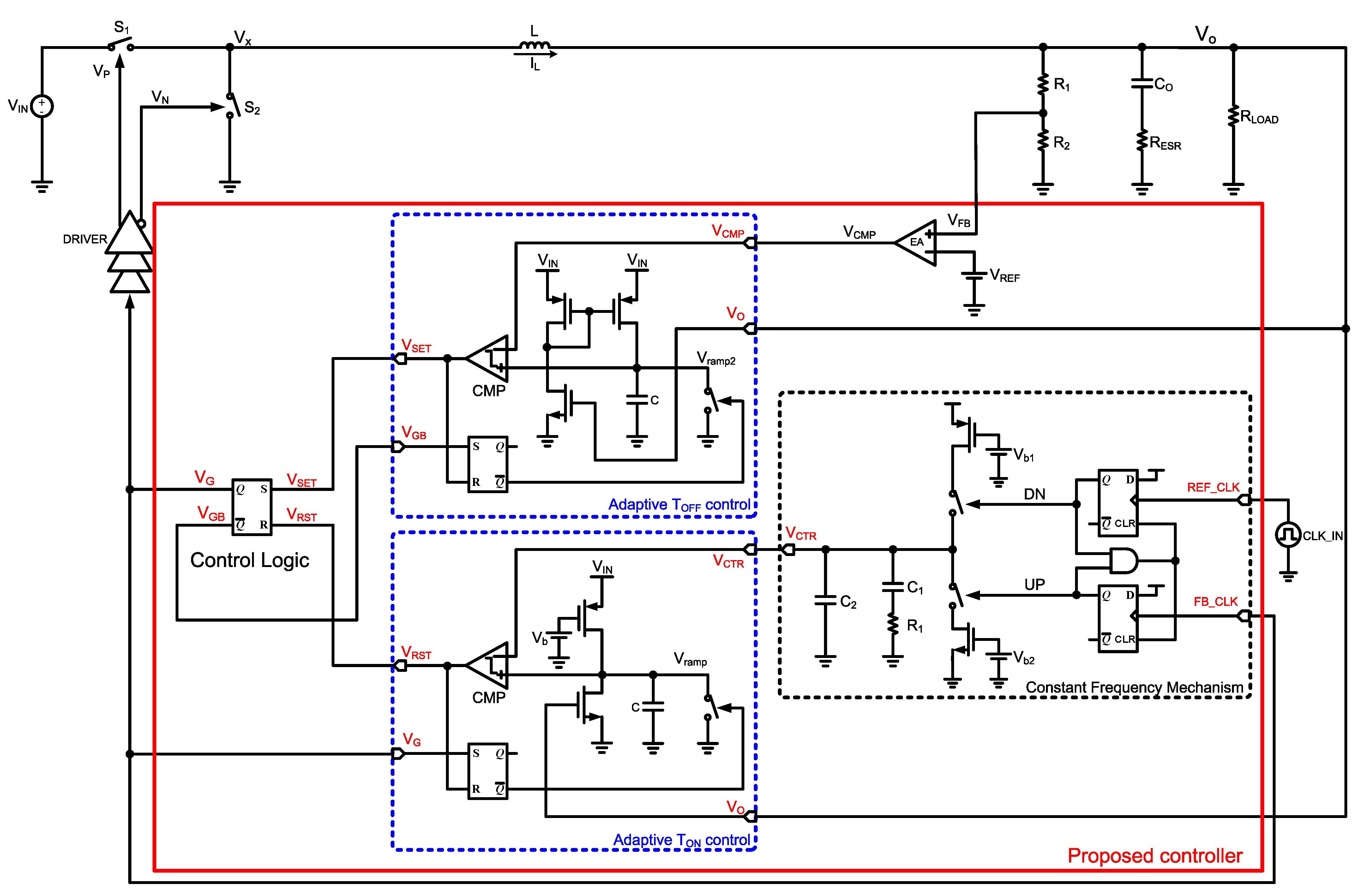
2.1. Scheme and Implementation
2.2. Operation Principle
- When the switch S1 is ON, and the other switch S2 is OFF.
- The inductor (L) is in the charging state, and the ON-time of S1 is controlled by the adaptive TON control block. In the adaptive TON control block, the ON-time is decided by Vramp and VCTR. The Vramp is the function of VIN and Vo, which replaces the conventional method that requires a current sensor to sense inductor current.
- When the switch S1 is OFF, and the other switch S2 is ON.
- The inductor (L) is in the discharging state, and the OFF-time of S1 is controlled by the adaptive TOFF control block. In the adaptive TOFF control block, the OFF-time is decided by Vramp2 and VCMP, both of which are the functions of the Vo. Since the Vo controls the OFF-time through two paths, the control scheme has good transient response.
- The operation of the constant frequency mechanism will make the REF_CLK and the FB_CLK equal. The REF_CLK can be set by the user. In this paper, the REF_CLK is set to 1 MHz.
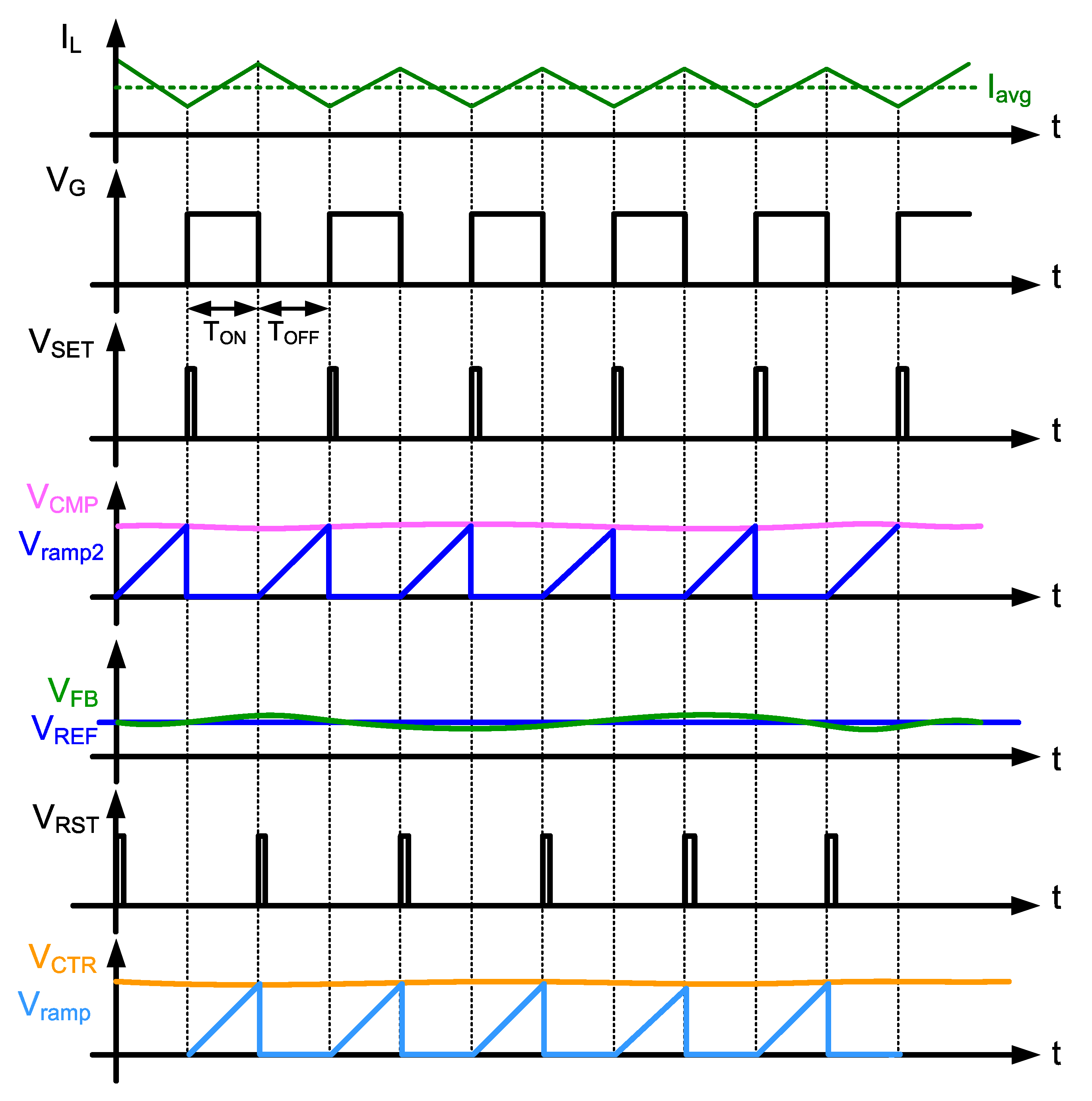
- In Figure 6, the IL is the inductor current. In the steady state, we can find that the IL is triangle wave, and the mean is Iavg. When the S1 is ON (i.e., VG is high), the IL is linearly rising and the inductor (L) is in the charging phase. On the contrary, the S1 is OFF (i.e., VG is low), the IL is linearly falling, and the inductor is in the discharging phase.
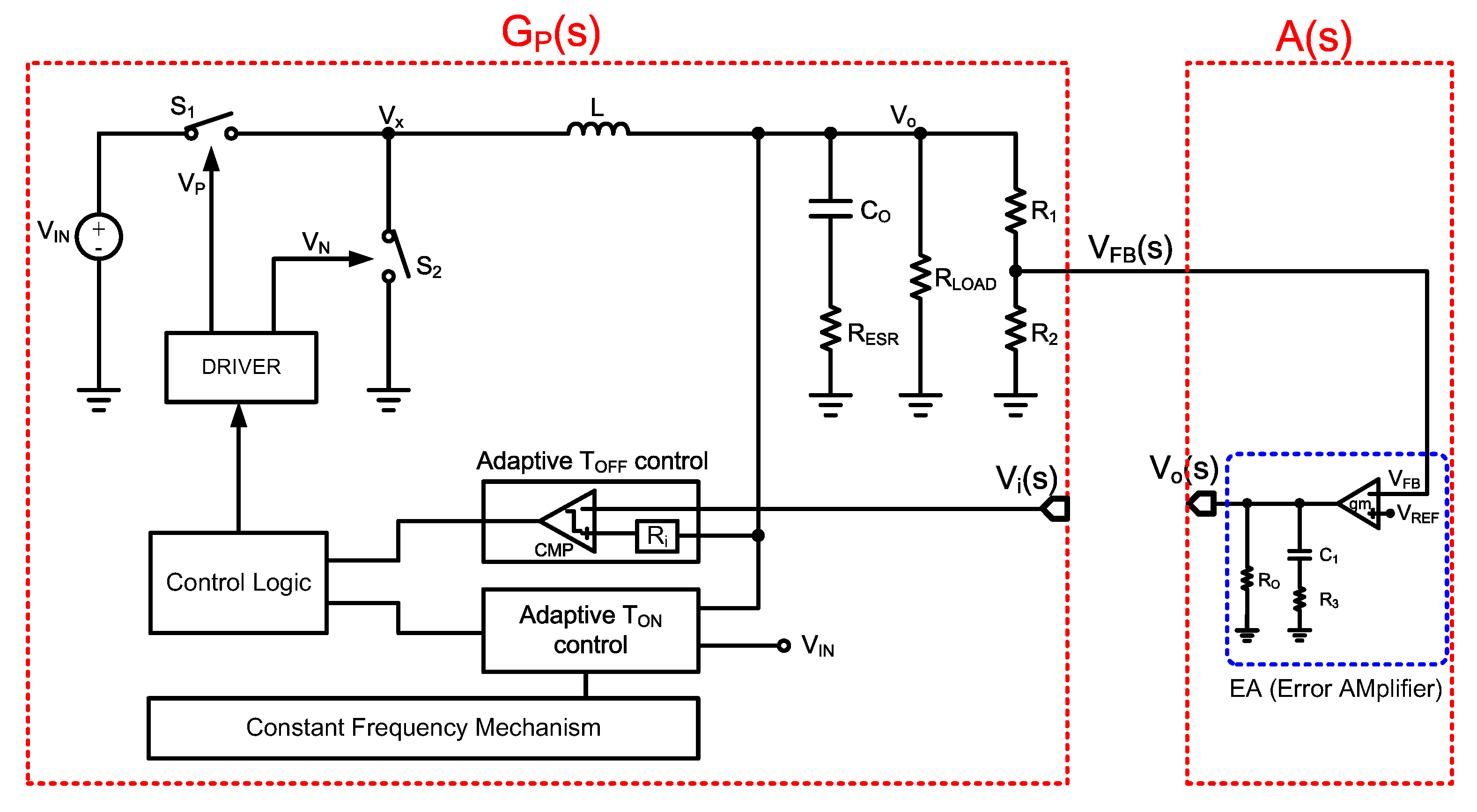
3. Mathematical Modeling and Components Selection
3.1. Mathematical Modeling
3.2. Components Selection
3.3. Implementation Processes
4. Simulation Results
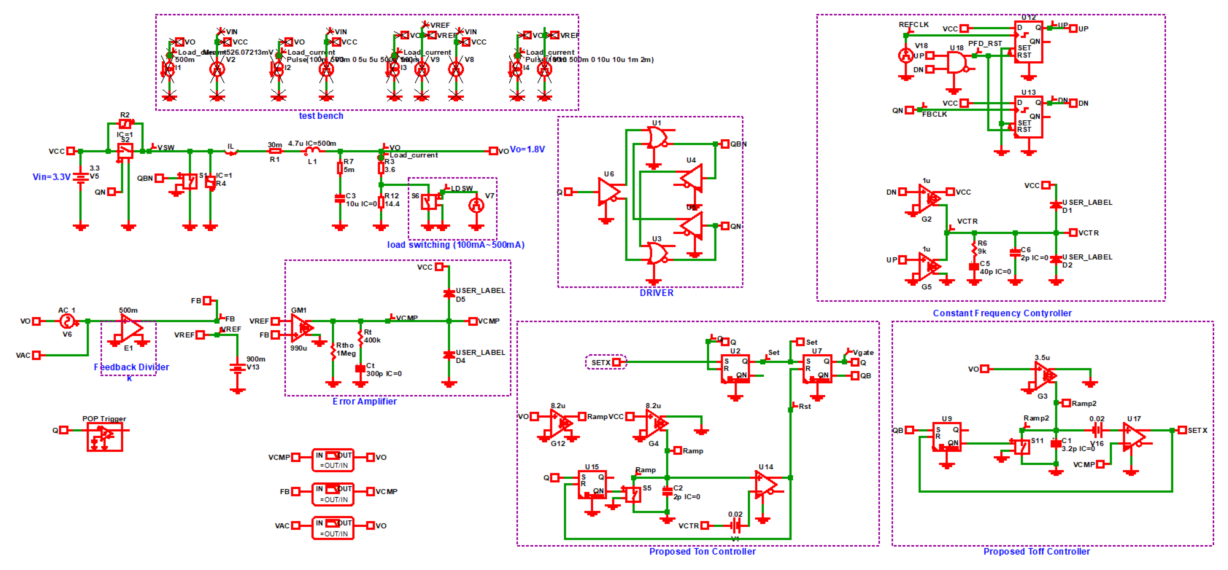
4.1. SIMPLIS Schematic
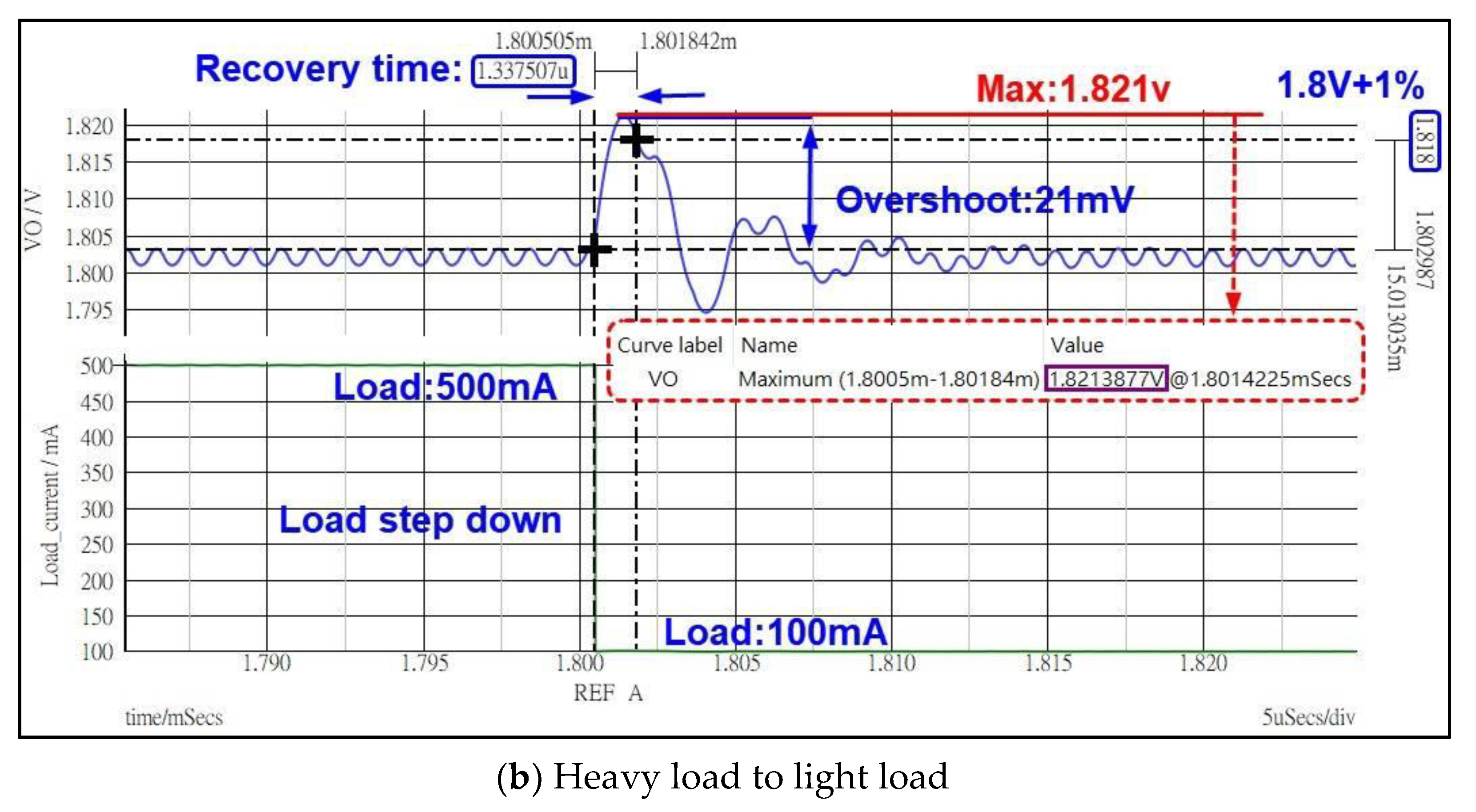
4.2. Transient Response
4.3. Load Regulation
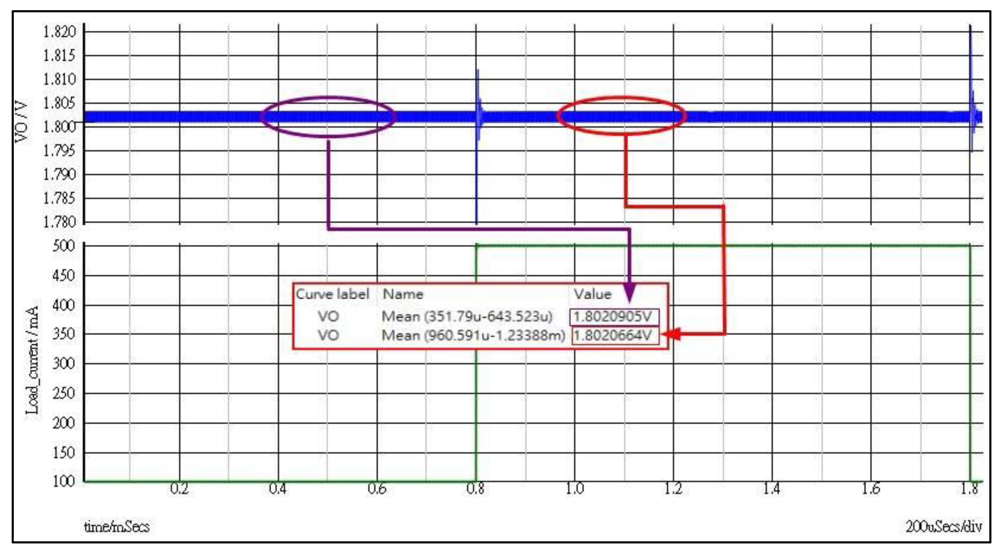
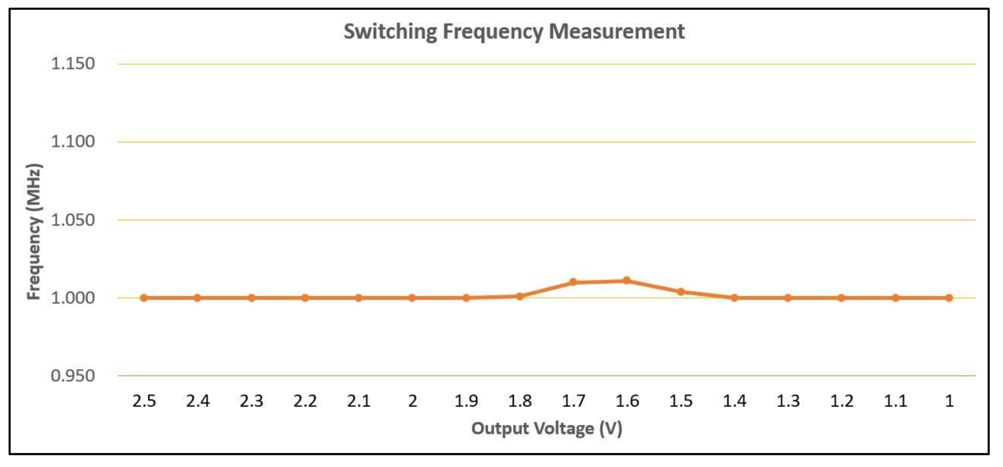
4.4. Switching Frequency Regulation
4.5. Performance Summary
- (a)
- For the parameter in recovery time, we can find that the proposed scheme is better than the simulation results of [15,21,22,23,24,25]. The measurement results of [11,26,27,28] are worse than the proposed scheme, and the numerical differences are large. For this purpose, one is the measurement result, and the other is the simulation result. This is the major difference.
- (b)
- For the parameter in undershoot/overshoot: this parameter is greatly affected by the load conditions and the output capacitor. For example, if the output capacitor is large, then the undershoot/overshoot is small. Or, if the load current step of the load conditions is small, then the undershoot/overshoot is small. Therefore, under the same test conditions, the performance of the proposed scheme is better than [15,21,22].
- (c)
- For the parameter in switching frequency, we can find that in most of the literature, the switching frequency is designed around 1 MHz.
- (d)

| References | 2018 [23] | 2020 [24] | 2021 [15] | 2021 [22] | 2022 [21] | This Work |
|---|---|---|---|---|---|---|
| Results | simulation | simulation | simulation | simulation | simulation | simulation |
| Control scheme | AOT | AOT | AOT | AOT | AOT | AOT |
| Process (μm) | 0.35 | 0.18 | 0.35 * | 0.18 * | 0.35 * | 0.18 * |
| Input voltage (V) | 12 | 3.3–5.0 | 3.0–3.6 | 3.0–3.6 | 3.0–3.6 | 3.0–3.6 |
| Output voltage (V) | 1.2 | 1.8 | 1.0–2.5 | 1.0–2.5 | 1.0–2.5 | 1.0–2.5 |
| Inductor (μH) | 1 | 1.5 | 4.7 | 4.7 | 4.7 | 4.7 |
| Output Capacitor (μF) | 47 | 20 | 10 | 10 | 10 | 10 |
| Switching Frequency (MHz) | 1 | 1 | 1 | 1 | 1 | 1 |
| Switching frequency variation (%) | N/A | N/A | N/A | 1 | 3.5 | 1.2 |
| Max. Load current (mA) | 5000 | 2000 | 500 | 500 | 500 | 500 |
| Load current step (mA) | 4000 | 800 | 400 | 400 | 400 | 400 |
| Undershoot/Overshoot (mV) | 20/26 | 13/14 | 23/26 | 20/24 | 21/30 | 21/21 |
| Recovery time (μs) (rise/fall) | <3 | 6/2 | 1.98/1.6 | 1.69/1.62 | 1.8/1.5 | 1.57/1.34 |
| References | 2019 [25] | 2021 [11] | 2021 [26] | 2021 [27] | 2022 [28] | |
| Results | measurement | measurement | measurement | measurement | measurement | |
| Control scheme | Current-Mode Hysteretic | Hysteretic PLL | COT | COT | AOT | |
| Process (μm) | 0.065 | 0.35 | 0.13 | 0.18 | 0.18 | |
| Input voltage (V) | 3.3 | 3.3–3.6 | 7–15 | 4.25–15 | 1.6–2.2 | |
| Output voltage (V) | 0.6–2.0 | 0.9–2.5 | 5–7 | 1.1 | 0.4–1.2 | |
| Inductor (μH) | 2.2 | 4.7 | 2.2 | 0.47 | 0.33 | |
| Output Capacitor (μF) | 10 | 10 | 10 | 47*3 | 10 | |
| Switching Frequency (MHz) | 1 | 1 | 2 | 0.5–1.25 | 3 | |
| Switching frequency variation (%) | N/A | 1 | N/A | 42 | N/A | |
| Max. Load current (mA) | 1500 | 600 | 2000 | 5000 | 500 | |
| Load current step (mA) | 900 | 400 | 2000 | 5000 | 450 | |
| Undershoot/Overshoot (mV) | 106/87 | 30/60 | 85/72 | 30/15.7 | 20/20 | |
| Recovery time (μs) (rise/fall) | 3.4/3.6 | 2.6/2.2 | 3/2.7 | 80/45 | 3.4/3.6 |
5. Conclusions
Author Contributions
Funding
Institutional Review Board Statement
Informed Consent Statement
Data Availability Statement
Conflicts of Interest
References
- Chen, J.-J.; Lu, M.-X.; Wu, T.-H.; Hwang, Y.-S. Sub-1-V Fast-Response Hysteresis-Controlled CMOS Buck Converter Using Adaptive Ramp Techniques. IEEE Trans. Very Large Scale Integr. (VLSI) Syst. 2012, 21, 1608–1618. [Google Scholar] [CrossRef]
- Chen, J.-J.; Hwang, Y.-S.; Chen, J.-H.; Ku, Y.-T.; Yu, C.-C. A New Fast-Response Current-Mode Buck Converter With Improved I2 -Controlled Techniques. IEEE Trans. Very Large Scale Integr. (VLSI) Syst. 2018, 26, 903–911. [Google Scholar] [CrossRef]
- Hwang, Y.S.; Chen, J.J.; Ku, Y.T.; Yang, J.Y. An Improved Optimum-Damping Current-Mode Buck Converter with Fast-Transient Response and Small-Transient Voltage using New Current Sensing Circuits. IEEE Trans. Ind. Electron. 2020, 68, 9505–9514. [Google Scholar] [CrossRef]
- Souza, A.F.; Tofoli, F.L.; Ribeiro, E.R. Switched Capacitor DC-DC Converters: A Survey on the Main Topologies, Design Characteristics, and Applications. Energies 2021, 14, 2231. [Google Scholar] [CrossRef]
- Seeman, M.D.; Sanders, S.R. Analysis and Optimization of Switched-Capacitor DC–DC Converters. IEEE Trans. Power Electron. 2008, 23, 841–851. [Google Scholar] [CrossRef]
- Deepa, K.; Saju, H.; Kumar, M. Soft switched flyback converter for smps applications. In Proceedings of the 2013 International Conference on Control Communication and Computing (ICCC), Thiruvananthapuram, India, 13–15 December 2013; pp. 475–478. [Google Scholar]
- Aharon, I.; Kuperman, A.; Aharon, I.; Shmilovitz, D. Analysis of Bi-Directional Buck-Boost Converter for Energy Storage Applications. In Proceedings of the IECON 2013—39th Annual Conference of the IEEE Industrial Electronics Society, Vienna, Austria, 10–13 November 2013; pp. 88–96. [Google Scholar]
- Gallo, C.A.; Tofoli, F.L.; Pinto, J.A.C. Two-Stage Isolated Switch-Mode Power Supply with High Efficiency and High Input Power Factor. IEEE Trans. Ind. Electron. 2010, 57, 3754–3766. [Google Scholar] [CrossRef]
- Seeman, M.D.; Ng, V.W.; Le, H.-P.; John, M.; Alon, E.; Sanders, S.R. A comparative analysis of Switched-Capacitor and inductor-based DC-DC conversion technologies. In Proceedings of the 2010 IEEE 12th Workshop on Control and Modeling for Power Electronics (COMPEL), Boulder, CO, USA, 28–30 June 2010. [Google Scholar]
- Huang, Q.; Zhan, C.; Burm, J. A 30-MHz Voltage-Mode Buck Converter Using Delay-Line-Based PWM Control. IEEE Trans. Circuits Syst. II Express Briefs 2018, 65, 1659–1663. [Google Scholar] [CrossRef]
- Chen, J.-J.; Hwang, Y.-S.; Ku, Y.-T.; Li, Y.-H.; Chen, J.-A. A Current-Mode-Hysteretic Buck Converter with Constant-Frequency-Controlled and New Active-Current-Sensing Techniques. IEEE Trans. Power Electron. 2020, 36, 3126–3134. [Google Scholar] [CrossRef]
- Chen, J.-J.; Hwang, Y.-S.; Lin, J.-Y.; Ku, Y. A Dead-Beat-Controlled Fast-Transient-Response Buck Converter With Active Pseudo-Current-Sensing Techniques. IEEE Trans. Very Large Scale Integr. (VLSI) Syst. 2019, 27, 1751–1759. [Google Scholar] [CrossRef]
- Chen, W.-W.; Chen, J.-F.; Liang, T.-J.; Wei, L.-C.; Ting, W.-Y. Designing a Dynamic Ramp With an Invariant Inductor in Current-Mode Control for an On-Chip Buck Converter. IEEE Trans. Power Electron. 2013, 29, 750–758. [Google Scholar] [CrossRef]
- Saini, D.K.; Reatti, A.; Kazimierczuk, M.K. Average Current-Mode Control of Buck DC-DC Converter with Reduced Control Voltage Ripple. In Proceedings of the 42nd Annual Conference of the IEEE Industrial Electronics Society, Florence, Italy, 23–26 October 2016; IECON: Florence, Italy, 2016. [Google Scholar]
- Chou, H.-H.; Chen, H.-L.; Fan, Y.-H.; Wang, S.-F. Adaptive On-Time Control Buck Converter with a Novel Virtual Inductor Current Circuit. Electronics 2021, 10, 2143. [Google Scholar] [CrossRef]
- Zhong, S.; Shen, Z. A Hybrid Constant On-Time Mode for Buck Circuits. Electronics 2021, 10, 930. [Google Scholar] [CrossRef]
- Nien, C.-F.; Chen, D.; Hsiao, S.-F.; Kong, L.; Chen, C.-J.; Chan, W.-H.; Lin, Y.-L. A Novel Adaptive Quasi-Constant On-Time Current-Mode Buck Converter. IEEE Trans. Power Electron. 2016, 32, 8124–8133. [Google Scholar] [CrossRef]
- Liu, P.-J.; Kuo, M.-H. Adaptive On-Time Buck Converter with Wave Tracking Reference Control for Output Regulation Accuracy. Energies 2021, 14, 3809. [Google Scholar] [CrossRef]
- Bari, S.; Li, Q.; Lee, F.C. A New Fast Adaptive On-Time Control for Transient Response Improvement in Constant On-Time Control. IEEE Trans. Power Electron. 2018, 33, 2680–2689. [Google Scholar] [CrossRef]
- Chou, H.-H.; Luo, W.-H.; Chen, H.-L.; Wang, S.-F. A Novel Buck Converter with Dual Loops Control Mechanism. Electronics 2022, 11, 1256. [Google Scholar] [CrossRef]
- Chou, H.-H.; Luo, W.-H.; Wang, S.-F. Design of the Buck Converter without Inductor Current Sensor. Electronics 2022, 11, 1484. [Google Scholar] [CrossRef]
- Chou, H.-H.; Chen, H.-L. A Novel Buck Converter with Constant Frequency Controlled Technique. Energies 2021, 14, 5911. [Google Scholar] [CrossRef]
- Zhen, S.; Zeng, P.; Chen, J.; Zhou, W.; Wang, J.; Luo, P.; Zhang, B. Transient Response Improvement of DC-DC Converter by Current Mode Variable on Time Control. In Proceedings of the 2018 IEEE 61st International Midwest Symposium on Circuits and Systems (MWSCAS), Windsor, ON, Canada, 5–8 August 2018. [Google Scholar]
- Jiang, C.R.; Chai, C.C.; Han, C.X.; Yang, Y.T. A high performance adaptive on-time controlled valley-current-mode DCDC buck converter. J. Semicond. 2020, 41, 062406. [Google Scholar] [CrossRef]
- Jeong, M.G.; Kang, J.G.; Park, J.; Yoo, C. A Current-Mode Hysteretic Buck Converter With Multiple-Reset RC-Based Inductor Current Sensor. IEEE Trans. Ind. Electron. 2019, 66, 8445–8453. [Google Scholar] [CrossRef]
- Ain, Q.; Khan, D.; Jang, B.G.; Basim, M.; Shehzad, K.; Asif, M. A High-Efficiency Fast Transient COT Control DC–DC Buck Converter With Current Reused Current Sensor. IEEE Trans. Power Electron. 2021, 36, 9521–9535. [Google Scholar] [CrossRef]
- Jeon, I.; Min, K.; Park, J.; Roh, J.; Moon, D.-J.; Kim, H.-R. A Constant On-Time Buck Converter with Fully Integrated Average Current Sensing Scheme. In Proceedings of the 2021 18th ISOCC, Jeju Island, Republic of Korea, 6–9 October 2021. [Google Scholar]
- Chen, J.-J.; Hwang, Y.-S.; Jiang, W.-M.; Lai, C.-H.; Ku, J. A New Improved Ultra-Fast-Response Low-Transient-Voltage Buck Converter With Transient-Acceleration Loops and V-Cubic Techniques. IEEE Access 2022, 10, 3601–3607. [Google Scholar] [CrossRef]


| Components | Value | Unit |
|---|---|---|
| Co | 10 | μF |
| L | 4.7 | μH |
| RESR | 5 | mΩ |
| RLOAD | 3.6/18 (for load switching) | Ω |
| R1 | 10 | MΩ |
| R2 | 10 | MΩ |
| Ro | 1 | MΩ |
| R3 | 400 | kΩ |
| C1 | 300 | pF |
| Parameter | Symbol | Conditions | Min | Typ | Max | Unit |
|---|---|---|---|---|---|---|
| Output capacitor | Co | ESR: 5 mΩ | 10 | μF | ||
| Inductor | L | DCR *: 30 mΩ | 4.7 | μH | ||
| Output voltage | Vo | 1.0 | 2.5 | V | ||
| Input supply voltage | Vin | 3.0 | 3.6 | V | ||
| Load current | Iload | 100 | 500 | mA | ||
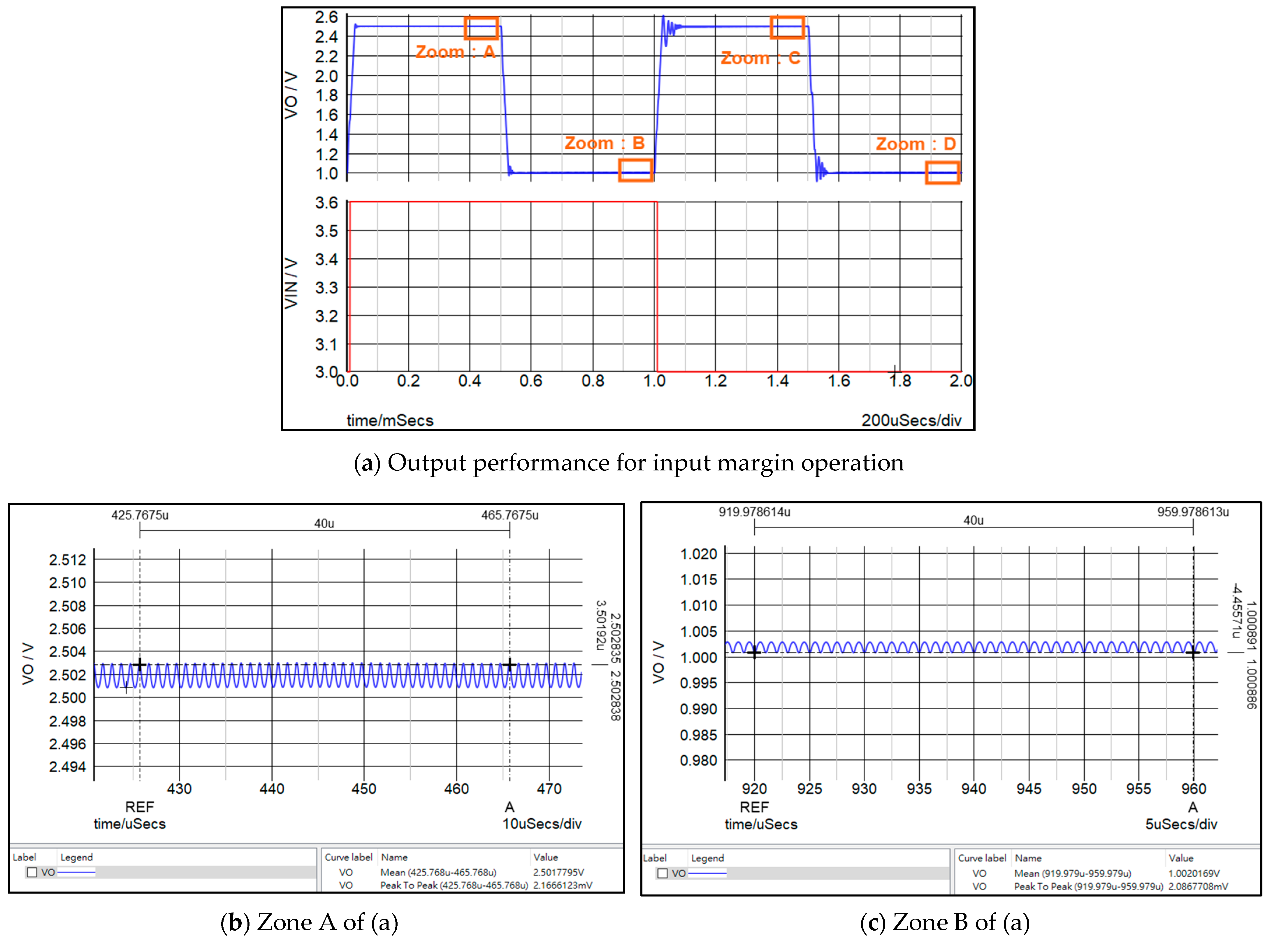
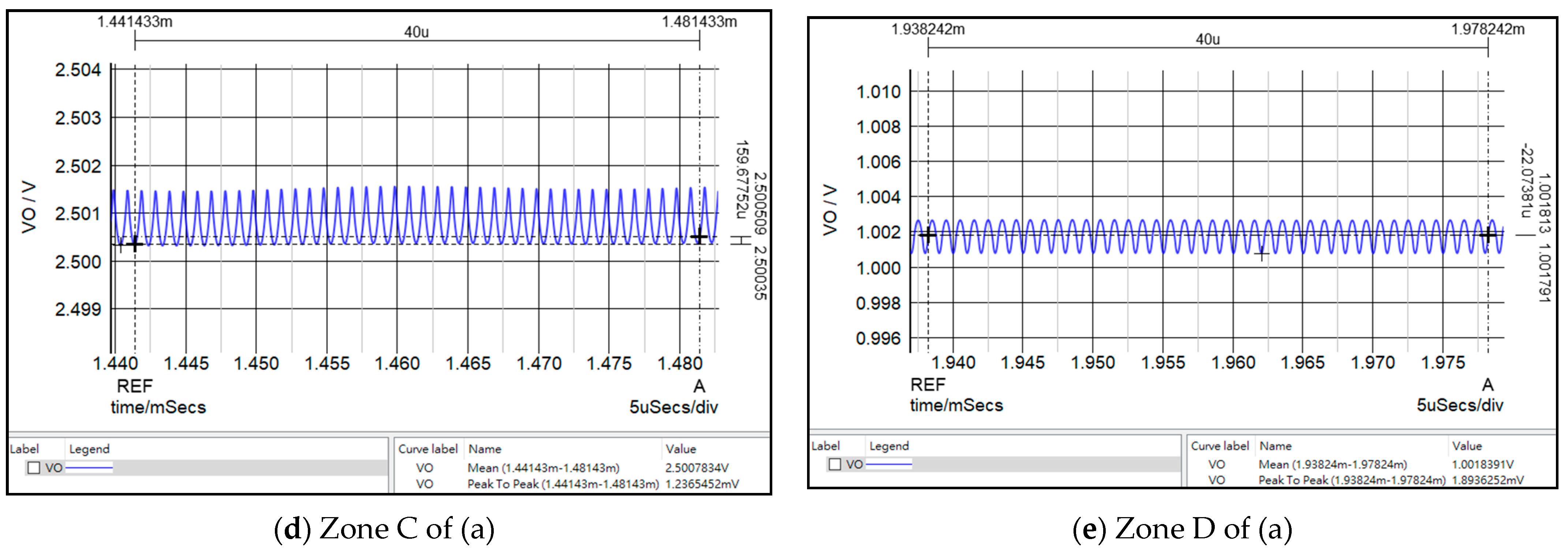
| Output ripple | Vpp | Vin = 3.6 V, Vo = 2.5 V | 2.2 | mV | ||
| Switching frequency | fsw | Load current: 500 mA @ Vin = 3.3 V, Vo = 1.0–2.5 V | 1 | MHz | ||
| Recovery time (step-up) | Tstep_up | Load current: 100 mA to 500 mA @ Vin = 3.3 V, Vo = 1.8 V | 1.57 | μs | ||
| Recovery time (step-down) | Tstep_dn | Load current: 500 mA to 100 mA @ Vin = 3.3 V, Vo = 1.8 V | 1.34 | μs | ||
| Overshoot | Vovshoot | Load current: 500 mA to 100 mA @ Vin = 3.3 V, Vo = 1.8 V | 21 | mV | ||
| Undershoot | Vunshoot | Load current: 100 mA to 500 mA @ Vin = 3.3 V, Vo = 1.8 V | 21 | mV |
Disclaimer/Publisher’s Note: The statements, opinions and data contained in all publications are solely those of the individual author(s) and contributor(s) and not of MDPI and/or the editor(s). MDPI and/or the editor(s) disclaim responsibility for any injury to people or property resulting from any ideas, methods, instructions or products referred to in the content. |
© 2023 by the authors. Licensee MDPI, Basel, Switzerland. This article is an open access article distributed under the terms and conditions of the Creative Commons Attribution (CC BY) license (https://creativecommons.org/licenses/by/4.0/).
Share and Cite
Chou, H.-H.; Chen, J.-Y.; Tseng, T.-H.; Yang, J.-Y.; Yang, X.; Wang, S.-F. A New Control Scheme for the Buck Converter. Appl. Sci. 2023, 13, 1991. https://doi.org/10.3390/app13031991
Chou H-H, Chen J-Y, Tseng T-H, Yang J-Y, Yang X, Wang S-F. A New Control Scheme for the Buck Converter. Applied Sciences. 2023; 13(3):1991. https://doi.org/10.3390/app13031991
Chicago/Turabian StyleChou, Hsiao-Hsing, Jian-Yu Chen, Tsung-Hu Tseng, Jun-Yi Yang, Xuan Yang, and San-Fu Wang. 2023. "A New Control Scheme for the Buck Converter" Applied Sciences 13, no. 3: 1991. https://doi.org/10.3390/app13031991