Article

Optimization Strategy for Output Voltage of CCM Flyback Converter Based on Linear Active Disturbance Rejection Control

1
Key Laboratory of Advanced Manufacturing and Automation Technology, Education Department of Guangxi Zhuang Autonomous Region, Guilin University of Technology, Guilin 541006, China
2
College of Mechanical and Control Engineering, Guilin University of Technology, Guilin 541006, China
*
Author to whom correspondence should be addressed.
Appl. Sci. 2023, 13(23), 12786; https://doi.org/10.3390/app132312786
Submission received: 23 October 2023 / Revised: 15 November 2023 / Accepted: 25 November 2023 / Published: 28 November 2023

Abstract

:
To solve the problem of system output voltage fluctuation caused by interferences such as load fluctuation and internal inductor parameter perturbation in a flyback converter, a second-order linear active disturbance rejection control (LADRC) strategy based on output voltage is proposed in this paper. A small-signal model of a CCM flyback converter is established, and the equivalent transfer function of voltage control based on second-order LADRC is derived. A second-order LADRC is constructed, and a parameter design method for the controller is proposed. The response characteristics of the output voltage of the converter under five internal and external disturbances of different control strategies are compared and studied using MATLAB R2022b/Simulink simulation software, and a CCM flyback converter experimental platform based on dSPACE is built to verify the corresponding comparative experiments. The simulation and experimental results jointly verify the superiority of the control strategy for the anti-interference and robustness of the output voltage of the CCM flyback converter.

1. Introduction

In recent years, with the rapid development of portable electronic devices such as smartphones and laptops, the performance requirements for switching power converters have increased [1,2]. As one of the main topologies of switching power converters, flyback converters are widely used in small and medium-sized power supply applications due to their advantages of simple topology, low cost, and high reliability [3,4,5,6,7]. Industrial equipment, lighting, electronics, and aerospace technology have increasingly complex requirements for power supply, and output voltage overshoot caused by factors such as load jump can easily lead to damage to the load and power supply [8]. Therefore, the research into the transient response characteristics and anti-interference performance of switching power converters is of great significance. The continuous conduction mode (CCM) flyback converter has a right-half-plane zero (RHPZ) characteristic, and its transient response characteristics and anti-interference performance need to be improved [8].
The robustness, adaptability, and stability of the system are crucial in the operation of power electronic converters. The control methods of power electronic converters are of great significance in improving the system’s load-bearing capacity, wide input voltage capacity, and anti-interference ability. At present, the application of classical PID control in power electronic converters is relatively mature and widespread and can meet general performance requirements [9,10]. This method relies on the control strategy of “eliminating this error by the error between the target and actual behavior”, and constructs a control signal based on the past, present, and future trends in the error, namely the proportional integral derivative of the error [11,12,13]. This method is simple and convenient, but this “simple processing” also places certain limitations on the controller, such as difficulty in solving the contradiction between speed and overshoot, and weak robustness. With the rapid development in power electronics technology, requirements for the performance of converters are gradually increasing. Therefore, it is necessary to seek a more superior control method to apply this performance.
The existence of a right-half-plane zero point in the CCM flyback converter makes the system appear nonlinear. When there is interference in the system, PID control is insufficient to balance the contradiction between speed and overshoot, and unstable phenomena may even occur. In response to these issues, many scholars have undertaken relevant research. Reference [14] reduces the error in feedback voltage by improving sampling accuracy in flyback converters, while reference [15] introduces specific algorithms to calculate voltage sampling values in the system and improve sampling accuracy. Neither were improved from the control algorithms; however, [16] improves the response speed of the converter by introducing a peak current inner loop control. However, in peak current mode, the duty cycle is controlled by many variables, such as input voltage, which increases the complexity and parameters of the control and also introduces noise; [17] introduces inner loop constant current control based on the PID control framework in the system, but this has the disadvantage of a complex control structure. There is relatively little research on the anti-interference control strategy for the output voltage of CCM flyback converters.
PID controllers are widely used in industrial control applications due to their simple configuration. However, to achieve high performance, adjustments must be made [18]. Active disturbance rejection control (ADRC) [19,20,21] was proposed by Han Jingjing, a researcher of the Chinese Academy of Sciences, in 1999. Through development, ADRC has been widely used. In terms of engineering applications, ADRC research has gradually penetrated into a large number of engineering and scientific research fields such as motor drive systems, aircraft, power systems, and robots [22,23,24,25,26,27,28,29,30,31]. Reference [22] applies ADRC to lane-keeping control in automotive autonomous driving. The application of ADRC in reference [25] for obstacle avoidance control of quadcopter aircraft reduces the impact of wind disturbance and measurement noise, and improves the accuracy of flight trajectory. Reference [26] introduced ADRC into the inverted pendulum system, achieving dual stable control of the swing angle and the position of the trolley. Reference [28] improves the current quality of the input grid of the photovoltaic three-phase grid connected inverter by applying ADRC. Reference [29] uses ADRC to ensure the displacement tracking accuracy of the robot’s robotic arm. Reference [30] utilizes ADRC control to reduce the impact of amplitude disturbance on hydraulic motor systems. The engineering applications of ADRC in different control objects fully demonstrate the superiority of its control performance, which is of great reference significance for further research on ADRC in optimizing the voltage regulation performance of CCM flyback converters.
This paper proposes a second-order LADRC strategy based on the output voltage to optimize the dynamic anti-interference performance of a CCM flyback converter. First, establish a small-signal model for the controlled object CCM flyback converter. Then, the basic framework of second-order LADRC is constructed, equivalent to a two-degree-of-freedom system. The controller parameter design method was constructed by analyzing the Bode diagram of its equivalent transfer function. A simulation model was built using MATLAB R2022b software, and it was compared with the PID control algorithm. Finally, a prototype of a 72 W flyback converter was constructed, and further comparative experiments were conducted using the dSPACE semi-physical simulation platform. The experimental results showed that the second-order LADRC strategy based on output voltage proposed in this paper effectively improves the anti-interference and robustness of the CCM flyback converter.
The main contributions of this article are as follows:
(1) A second-order linear active disturbance rejection control method is proposed for the anti-interference performance of the output voltage of CCM flyback power converter.
(2) The proposed control scheme includes equating the controller to a two degree of freedom system and establishing a parameter tuning method for designing controller parameters by analyzing the Bode diagram of its equivalent transfer function, reducing the parameter trial work of engineers when applying the control algorithm.
(3) In order to validate the proposed design method, the LADRC-CCM flyback converter system was simulated in Simscape Electrical of MATLAB and compared with the traditional PID scheme.
(4) This article provides a detailed introduction on how to combine the hardware of power electronic converters with the dSPACE semi physical simulation platform for experiments, reducing the time for physical construction, accelerating the experimental process, and providing reference for other researchers in experimental methods.
(5) Compared with the traditional control algorithm PID, the proposed second-order LADRC outperforms the traditional PID controller in terms of load disturbance and other aspects in the designed situation.
(6) The research results provide important references for the promotion and design of ADRC in power electronic converters, and also provide a necessary theoretical basis for further optimizing the control methods of CCM flyback converters.
The rest of this article is organized as follows: The mathematical model of the CCM flyback converter is obtained in Section 2. Section 3 provides an overview of the LADRC controller. This section also elaborates on the method of controller parameter tuning. Section 4 introduces the simulation and experiment of the designed control algorithm applied in the converter, and compares and analyzes the results. Finally, the conclusion is drawn in Section 5.

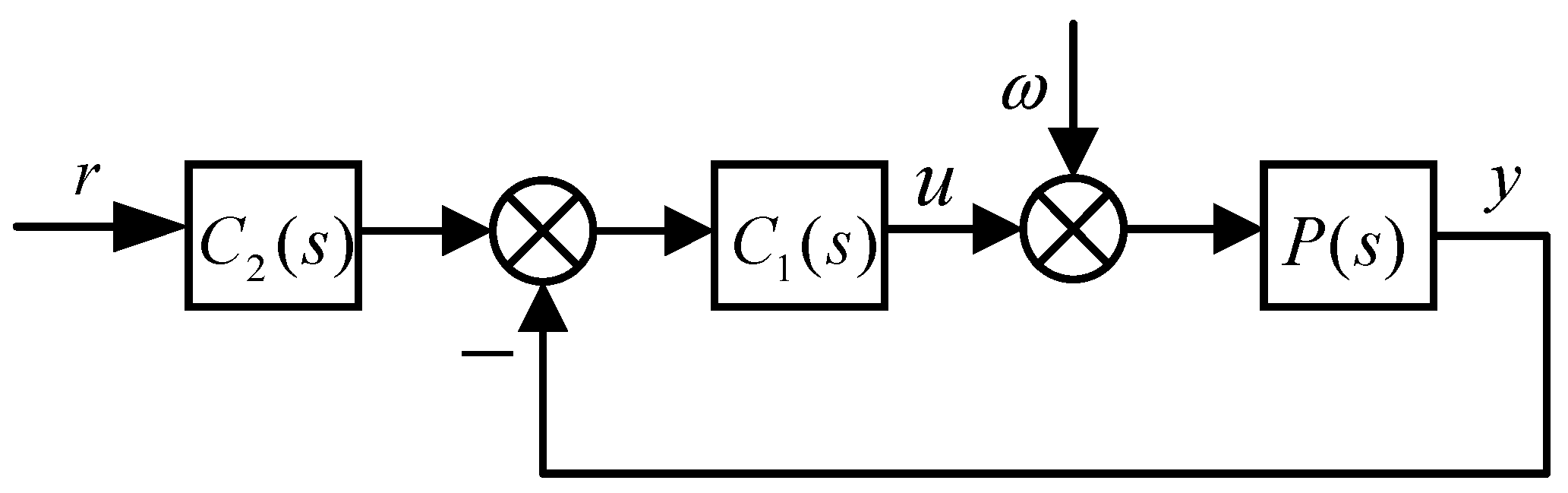
2. Small-Signal Model

The flyback converter is divided into two operating modes according to the continuous or intermittent condition of the primary current: if the primary current reaches zero, it is called Discontinuous Conduction Mode (DCM); if the primary current does not reach zero, it is called continuous conduction mode. In this paper, the main power circuit diagram of a CCM single-ended flyback converter is shown in Figure 1, in which Q is the main power switch, D1 is the diode, C is the output filter capacitor, R L is the load, L m is the transformer excitation inductor, u in is the input voltage, u o is the output voltage, i 1 and i in are the excitation current and the primary input current, n is the ratio of turns on the original secondary side of the transformer, and d is the on-duty cycle of the main power switch Q.
When the main power switch Q is on, the primary side of the transformer stores energy, the current i 1 rises, the diode D1 on the secondary side is in the cut-off state, and the output voltage u o is kept constant by the capacitor C . At this point:
{ u Q ( t ) = 0 u L ( t ) = u in ( t ) i C ( t ) = u o ( t ) R L i in ( t ) = i 1 ( t )
where u Q is the drain-to-source voltage of the main power switch Q, u L is the primary voltage of the transformer, and i C is the current flowing through the output filter capacitor C .
When the main power switch Q is turned off, the primary side of the transformer releases energy, the excitation current i 1 decreases, the diode D1 on the secondary side is in the conduction state, and the primary side transmits energy to the secondary side. At this point:
{ u L ( t ) = u o ( t ) n i C ( t ) = i 1 ( t ) n u o ( t ) R L i in ( t ) = 0
The key waveforms of CCM flyback converter are shown in Figure 2 [32]. T S , T on , and T off are the switching period, turn-on time, and turn-off time of the main power switch Q separately.
In this paper, the state-space averaging method is used to build the average model of the transformer primary voltage u L ; the current i C of the output filter capacitor C and the input current u in is:
{ u L ( t ) = d ( t ) u in ( t ) d ( t ) u o ( t ) n i C ( t ) = d ( t ) i 1 ( t ) n u o ( t ) R L i in ( t ) = d ( t ) i 1 ( t )
Namely
{ L m d i 1 ( t ) d t = d ( t ) u in ( t ) d ( t ) u o ( t ) n C d u o ( t ) d t = d ( t ) i 1 ( t ) n u o ( t ) R L i in ( t ) = d ( t ) i 1 ( t )
Here, d + d = 1 ; d is the off-duty cycle of the main power switch Q.
The system adds perturbations i ^ 1 , u ^ o , d ^ , and u ^ in so that the instantaneous value is:
{ i 1 ( t ) = [ I 1 + i ^ 1 ( t ) ] u o ( t ) = [ V o + u ^ o ( t ) ] d ( t ) = [ D + d ^ ( t ) ] u in ( t ) = [ V in + u ^ in ( t ) ]
Combining Formulas (4) and (5):
L m d [ I 1 + i ^ 1 ( t ) ] d t = [ D + d ^ ( t ) ] [ V in + u ^ in ( t ) ] [ D d ^ ( t ) ] [ V o + u ^ o ( t ) ] n
where D + D = 1 , and D and D are the on-duty cycle and off-duty cycle of the main power switch Q during the steady state of the system.
In the same way, the output voltage is processed, ignoring the high-order infinitesimals, and the small-signal AC model after linearization of the CCM flyback converter is obtained by the Laplace transform:
{ s L m i ^ 1 ( s ) = D u ^ in ( s ) D u ^ o ( s ) n + [ V in + V o n ] d ^ ( s ) s C u ^ o ( s ) = D i ^ 1 ( s ) n u ^ o ( s ) R L I 1 d ^ ( s ) n s C u ^ o ( s ) = D i ^ 1 ( s ) n u ^ o ( s ) R L I 1 d ^ ( s ) n
The transfer function from system output voltage u o to duty cycle d is:
G vd ( s ) = V ^ o ( s ) d ^ ( s ) = D n ( V in + V o n ) s L m V o R L D L m C s 2 + L m R L s + ( D n ) 2 = L m V o R L D ( D n ( V in + V o n ) R L D L m V o s ) L m C s 2 + L m R L s + ( D n ) 2
From Equation (8), it can be seen that the transfer function from the output voltage u o to the duty cycle d of the CCM mode flyback converter has a right-half-plane zero.

3. Parameter Design of Anti Disturbance Voltage Control System

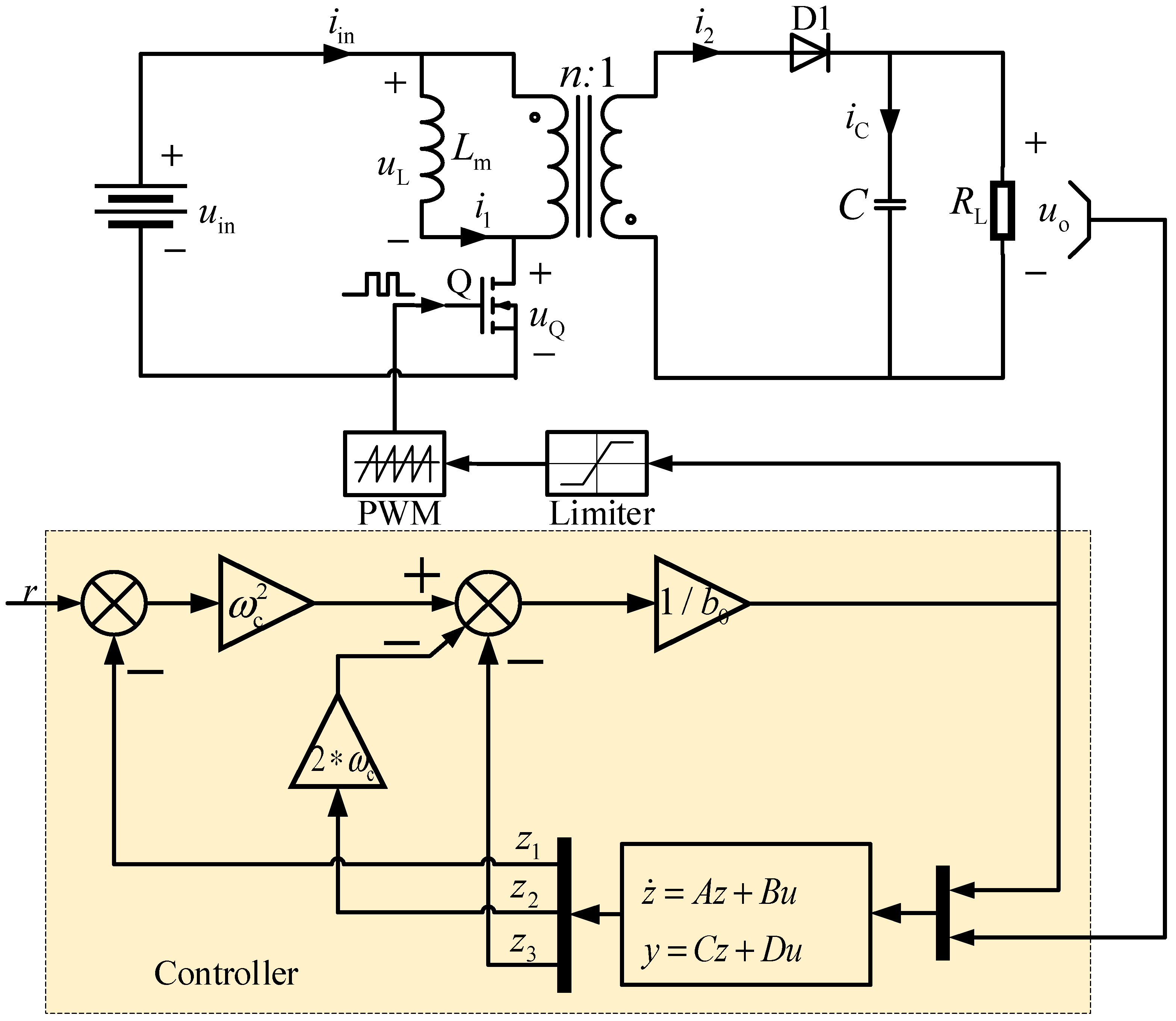
3.1. LADRC Basic Framework

The block diagram of the second-order LADRC system is shown in Figure 3.
The order selection of the LADRC is generally the same as the relative order of the controlled object [33]. From the small-signal model of the CCM flyback converter in the previous section, it can be seen that the converter can be regarded as a second-order control object. Therefore, a second-order LADRC strategy is designed to perform anti-interference control analysis on the controlled object. The model of the controlled object CCM flyback converter is:
y ¨ = b 0 u + f
where b 0 is the control gain, and f is the total unknown disturbance of the system, including the internal and external disturbances of the system.
In Formulas (9)–(11) and (13), x ˙ represents the first derivative of the variable, and x ¨ represents the second derivative of the variable.
Introducing the state variable z 1 = y ,   z 2 = y ˙ and the extended state z 3 = f , Equation (9) has:
{ z ˙ 1 = z 2 , z ˙ 2 = z 3 + b 0 u , z ˙ 3 = f ˙ , y = z 1
Establish a linear extended state observer (LESO):
{ z ^ ˙ 1 = β 1 ( y z ^ 1 ) + x ^ 2 , z ^ ˙ 2 = β 2 ( y z ^ 1 ) + x ^ 3 + b 0 u , z ^ ˙ 3 = β 3 ( y z ^ 1 )
where β 1 , β 2 , and β 3 are three adjustable LESO gains.
To compensate for the observed values of the extended state observer and the total disturbance obtained in real-time to the control variables, the linear state error feedback control (LSEF) is set to:
u = 1 b 0 [ I 2 ( r z ^ 1 ) I 1 x ^ 2 z ^ 3 ]
where I 1 and I 2 represent LSEF adjustable parameters.
LESO and LSEF form second-order LADRC, substituting (13) into (12), with:
{ z ^ ˙ 1 = β 1 z ^ 1 + z ^ 2 + β 1 y z ^ ˙ 2 = ( β 2 + I 2 ) z ^ 1 I 1 z ^ 2 + β 2 y + I 2 r z ^ ˙ 1 = β 3 z ^ 1 + β 3 y

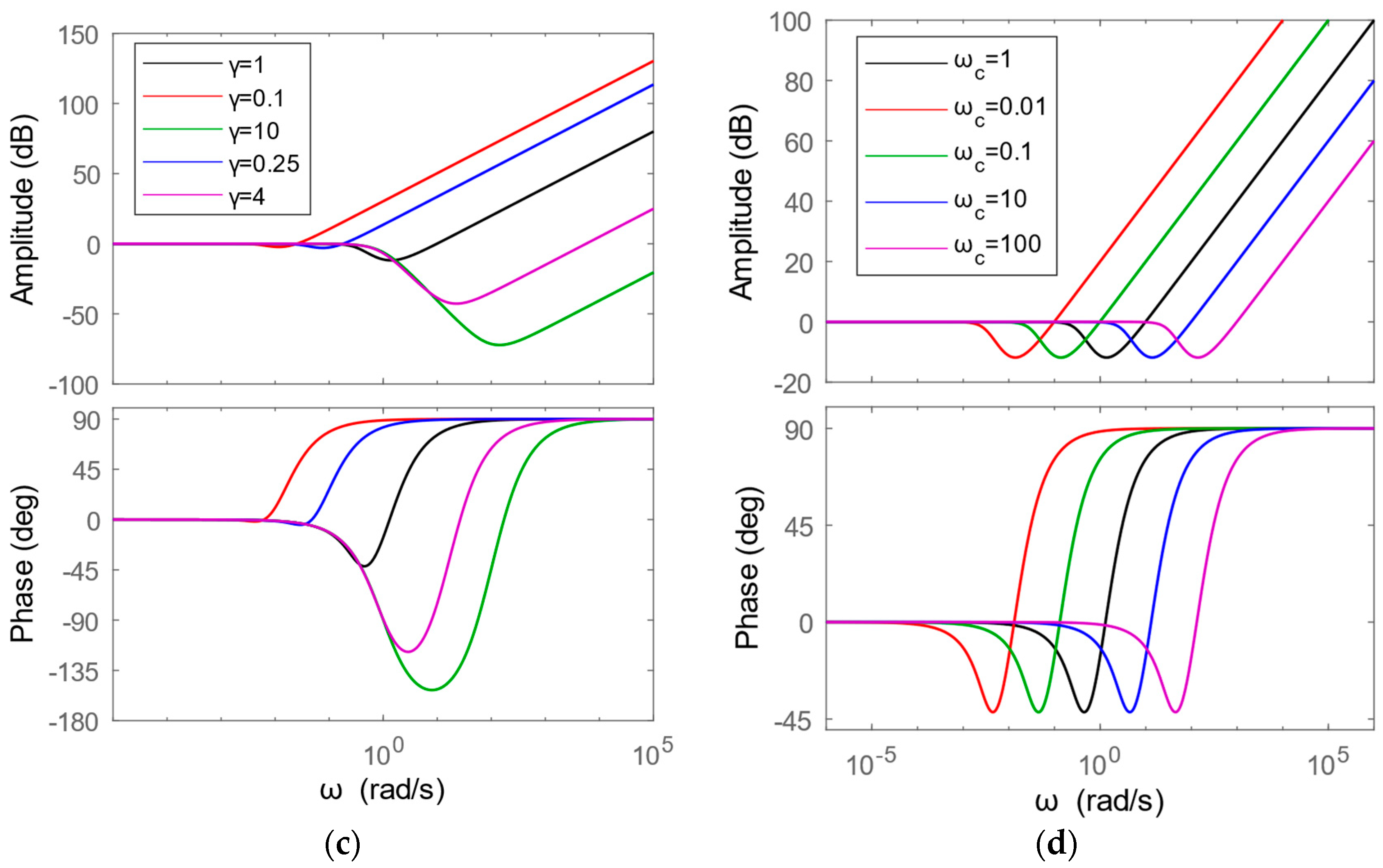
3.2. Parameter Design of Second-Order LADRC System

From Equations (12) and (13), the transfer functions from controller output u to system output y , and from controller output u to system input r can be obtained:
U ( s ) Y ( s ) = ( β 1 I 2 + β 2 I 1 + β 3 ) s 2 + ( β 2 I 2 + β 3 I 1 ) s + β 3 I 2 b 0 s [ s 2 + ( β 1 + I 1 ) s + β 1 I 1 + β 2 + I 2 ]
U ( s ) R ( s ) = I 2 ( s 3 + β 1 s 2 + β 2 s + β 3 ) b 0 s [ s 2 + ( β 1 + I 1 ) s + β 1 I 1 + β 2 + I 2 ]
The equivalent two-degree-of-freedom control block diagram of second-order LADRC is shown in Figure 4, where C 1 ( s ) is the feedback controller transfer function, C 2 ( s ) is the tracker transfer function, and P ( s ) is the transfer function of the controlled flyback converter. The expressions for C 1 ( s ) and C 2 ( s ) are as follows:
C 1 ( s ) = ( β 1 I 2 + β 2 I 1 + β 3 ) s 2 + ( β 2 I 2 + β 3 I 1 ) s + β 3 I 2 b 0 s [ s 2 + ( β 1 + I 1 ) s + β 1 I 1 + β 2 + I 2 ]
C 2 ( s ) = I 2 ( s 3 + β 1 s 2 + β 2 s + β 3 ) b 0 s [ s 2 + ( β 1 + I 1 ) s + β 1 I 1 + β 2 + I 2 ]
For the second-order LADRC system, the feedback gain and observer control adopt a bandwidth tuning method, introducing LESO bandwidth ω o and controller bandwidth ω c , so that
{ I 1 = 2 ω c , I 2 = ω c 2 , β 1 = 3 ω o , β 2 = 3 ω o 2 , β 3 = ω o 3 ,
Define bandwidth center ω f = ω c ω o , bandwidth ratio α = ω o / ω c , and γ = α .
Convert Equations (16) and (17) to:
C 1 ( s ) = K 1 b 0 s 1 ω 1 2 s 2 + 2 ζ 1 ω 1 s + 1 1 ω 2 s 2 + 2 ζ 2 ω 2 s + 1
C 2 ( s ) = 1 ( γ ω f ) 3 s 3 + 3 ( γ ω f ) s 2 + 3 γ ω f s + 1 1 ω 1 2 s 2 + 2 ζ 1 ω 1 s + 1
where
{ K 1 = ω f 3 γ 3 1 + 6 γ 2 + 3 γ 4 , ζ 1 = 2 γ 2 + 3 2 3 + 6 γ 2 + γ 4 , ζ 2 = 3 γ 2 + 2 2 1 + 6 γ 2 + 3 γ 4 , ω 1 = ω f γ 3 + 6 γ 2 + γ 4 , ω 2 = ω f 1 + 6 γ 2 + 3 γ 4 γ , ω m = ω 1 ω 2 = 1 + 6 γ 2 + 3 γ 4 3 + 6 γ 2 + γ 4 ω f
Under different bandwidth ratios γ and controller bandwidths ω c , in order to maintain generality, the control variable gain b 0 = 1 is used to obtain the Bode diagram of the equivalent feedback controller transfer function C 1 ( s ) and the tracker transfer function C 2 ( s ) of the system, as shown in Figure 5.
From Figure 5a,b, it can be seen that controller C 1 ( s ) is a series second-order lead correction unit, so the maximum phase angle of the system is relatively large. Overall, it shows that the system can provide a lead angle, and the phase compensation that can be provided is the smallest when the bandwidth ratio γ = 1 , that is, the controller bandwidth ω c = ω o is the smallest. The larger the difference between ω c and ω o , the greater the phase compensation; the phase angle between γ and 1 / γ is the same, and the farther away γ is from 1, the greater the phase compensation. The amplitude frequency characteristic curve has two turning frequencies, namely ω < ω f and ω > ω f . At frequency ω r , the slope of the amplitude frequency characteristic curve +1 and the phase close to the maximum can be provided. At the same time, when the bandwidth ratio γ is fixed and only the controller bandwidth ω c is changed, the amplitude frequency phase frequency curve of the compensator shifts to the left or right accordingly. The larger the bandwidth ratio γ , the more obvious the hysteresis effect. To achieve better phase compensation effect, compensation is carried out at frequency ω r .
As shown in Figure 5c,d, the tracker transfer function C 2 ( s ) has a unit gain in the low frequency range, while in the high frequency range it manifests as a first-order differential link with a slope of +1. Similarly, when the bandwidth ratio γ is fixed and only the controller bandwidth ω c is changed, the amplitude frequency phase frequency curve of the compensator shifts to the left and right accordingly.
For this converter, the system is required to pass through a frequency ω x of 1/10 of the operating frequency after compensation, i.e., ω x = 5.969 × 10 4   rad / s . If the bandwidth center r requires the system to compensate for the system phase margin ϕ 30 ° , then the feedback controller C 1 ( s ) needs to provide the phase at the bandwidth center ω f : C 1 ( j ω f ) = 180 ° + ϕ P ( s ) = 37.1 ° .
At this point, there are two ways to determine the bandwidth ratio γ . If γ > 1, then γ = 1.8484; If γ < 1 is taken, then γ = 0.541, and both have the same phase compensation angle. From Figure 5c, it can be seen that when γ < 1, the phase lag effect of C 2 ( s ) is not significant, and the system response is faster than when γ > 1. Therefore, in this paper, γ = 0.541 is used, so ω c = ω f / γ = 110 , 330   rad / s , ω o = ω f γ = 32 , 293   rad / s .
By setting the bandwidth center ω f = ω x to adjust the parameter b 0 , that is, after compensation ω f = ω x is the system amplitude frequency crossing frequency, the control gain can be obtained.
By setting the bandwidth center ω f = ω x to adjust the parameter b 0 , that is, after compensation ω f = ω x is the system amplitude frequency crossing frequency, at which point | C o ( j ω f ) P ( j ω f ) | = 1 , the control gain of b 0 = 1.3636 × 10 13 , can be obtained.

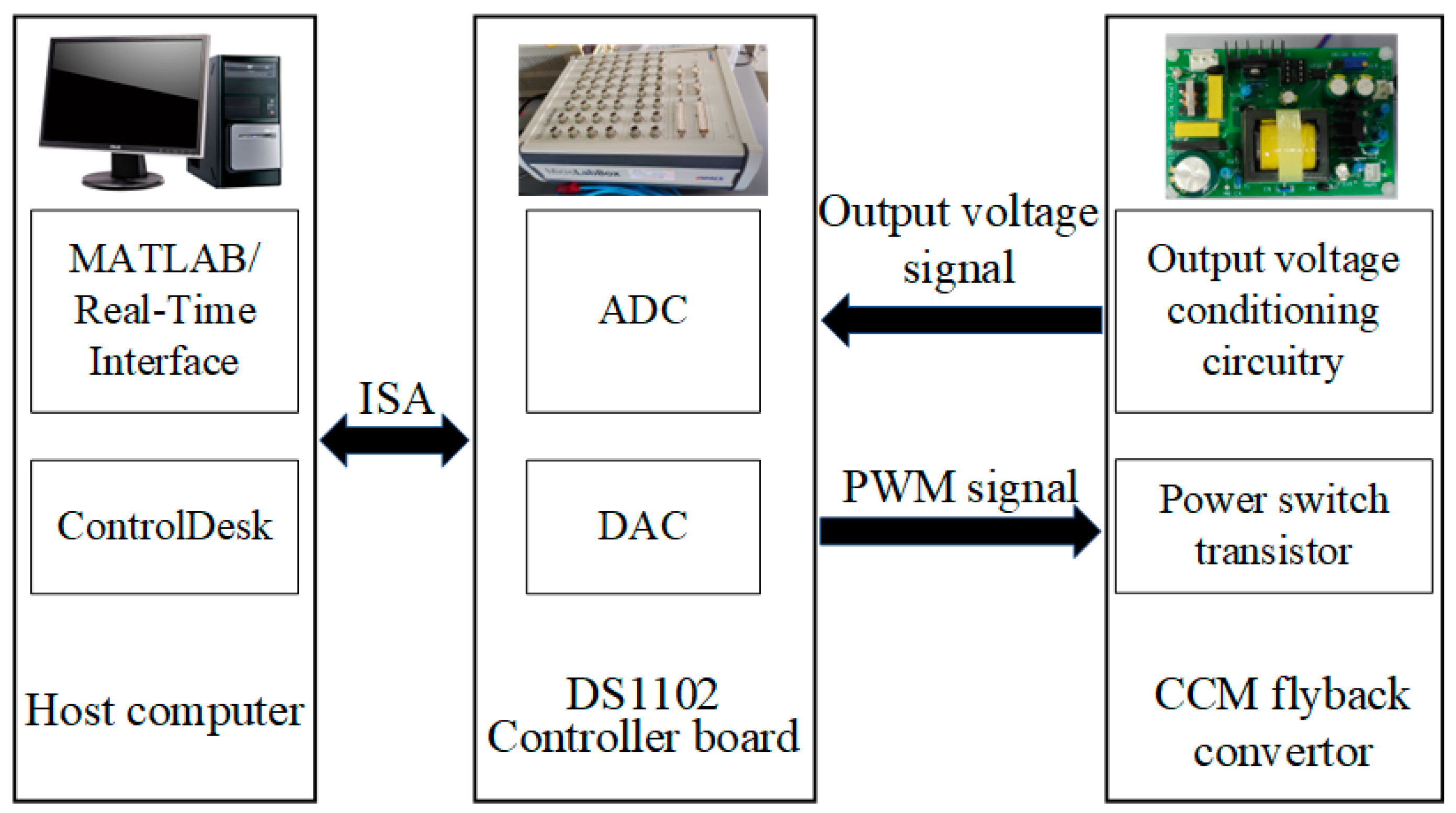
4. Simulation and Experimental Validation

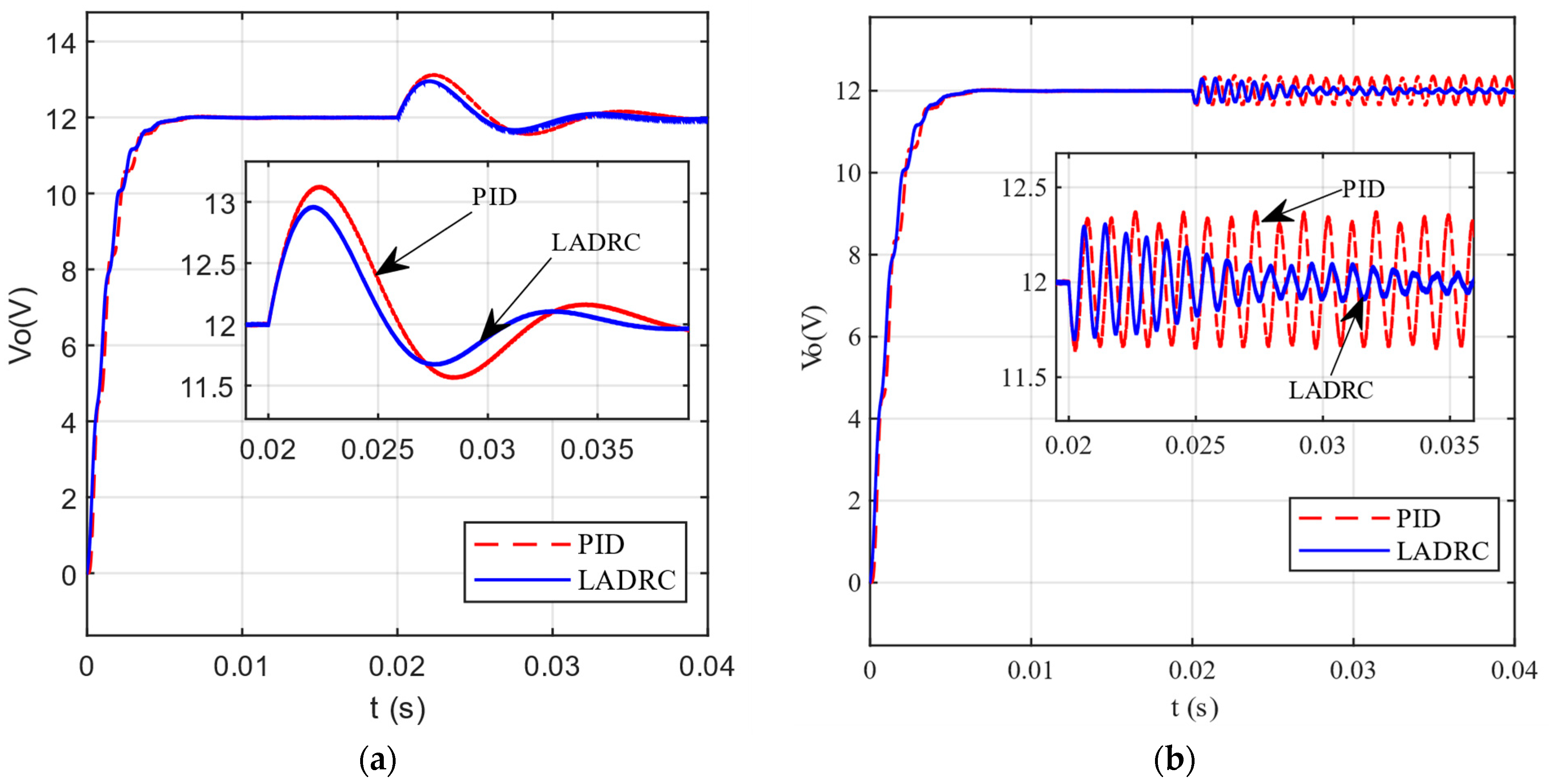
4.1. Comparison and Verification of Simulation Results

In order to analyze the anti-interference control effect of the control strategy on the CCM flyback converter, this paper uses MATLAB R2022b simulation software to build a simulation model of the CCM flyback converter. The specific electrical parameters are shown in Table 1. Figure 6 shows the block diagram of the converter with the proposed control method.
The effects of input voltage u in jump, load R L jump, and internal parameter L m fluctuation of the converter on the output voltage of the designed converter were simulated. At the same time, PID control algorithms were compared and simulated for the system under the same internal and external conditions. By adjusting the controller parameters of the two control algorithms, the adjustment time and overshoot range of the output voltage response of the converter system are roughly the same, in order to compare the suppression ability of the two control strategies on output voltage fluctuations when the system is subjected to internal and external disturbances. Figure 7 shows the control simulation results of two control strategies.
Figure 7a shows the response waveform of the output voltage V o of the converter when the load suddenly drops by 50% from the rated load 72 W, i.e., jumps to 36 W. Figure 7b shows the response waveform of the system output voltage V o when the rated load 72 W suddenly increases by 40%, i.e., jumps to 100.8 W. It can be seen that when the load suddenly drops, the output voltage fluctuation range of the second-order LADRC is smaller, with a maximum peak of 12.96 V, a minimum peak of 11.68 V, and an overshoot of 8%. The maximum peak value during PID control is 13.13 V, the minimum peak value is 11.57 V, and the overshoot is 9.42%. When the load suddenly rises, the system can gradually recover a stable 12 V output voltage under second-order LADRC, while the system output voltage under PID control continuously fluctuates between 12.36 V and 11.66 V.
Figure 7c,d show the dynamic changes of the output voltage when the input voltage suddenly increases by 6.43% and decreases by 6.43%. Meaning, when the output voltage suddenly rises from 311 V by 20 V and drops by 20 V. From the figure, when the input voltage suddenly rises, the maximum output voltage jump of the converter under second-order LADRC is 12.91 V, and the overshoot is 7.58%; the maximum output voltage under PID control is 13.29 V, with an overshoot of 10.75%. When the input voltage drops suddenly, the minimum output voltage drop of the flyback converter under second-order LADRC is 11.65 V, accounting for 2.92% of the steady-state value; under PID control, the minimum output voltage drop is 11.61 V, accounting for 3.25% of the steady-state value. Under second-order LADRC, the system output voltage drop is even smaller.
Figure 7e shows the internal parameters of the system. The excitation inductance L m of the transformer jumps by 8.62%, which is the output voltage response waveform when it jumps from 580 μ F to 530 μ F . When the excitation inductance of the transformer jumps, the overshoot of the system output voltage fluctuation under second-order LADRC is 3.25%, and the overshoot under PID control is 3.83%. It can be seen that the system has more advantages in resisting internal parameter disturbances under second-order LADRC.
The simulation results show that using LADRC not only achieves good and fast output without overshoot but also has better adaptability and robustness to input voltage, load jump, and self-parameter jump under second-order LADRC compared to PID control.

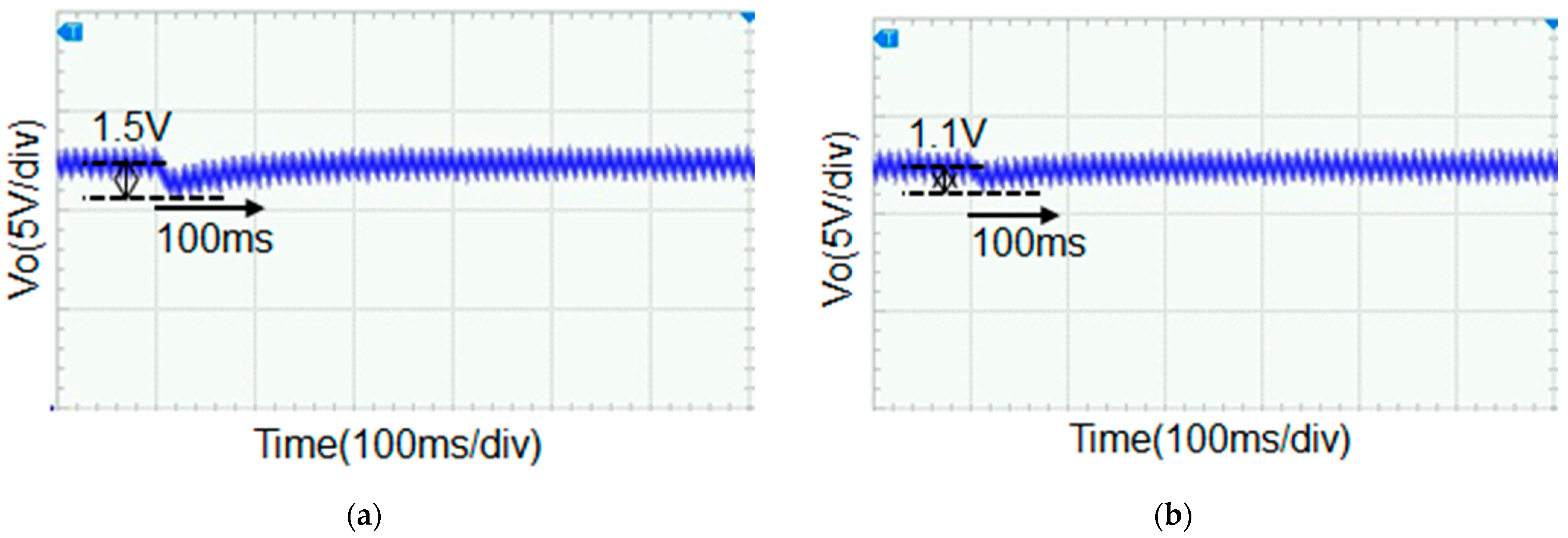
4.2. Comparative Verification of Experimental Results

Based on the above simulation parameters, a 72 W flyback converter experimental platform was established based on second-order LADRC and PID control. The DSP control board DS1102 from DSPACE company was used as the main control unit in the experiment. The second-order LADRC strategy and PID control proposed in this article are compiled into a DS1102 control program through a Simulink block diagram, generating PWM signals that directly control the power switch of the flyback converter through the driving circuit. The overall framework of the experimental platform is shown in Figure 8, and the flyback converter experimental platform based on dSPACE is shown in Figure 9.
The experimental parameters of the main circuit of the flyback converter are shown in Table 1; the digital controller parameters and simulation parameters are the same. The comparative experimental results are shown in Figure 10 and Figure 11. Figure 10a,b show the waveform of the system output voltage during load sag under PID and second-order LADRC, respectively. The output voltage fluctuation under PID control is 3.4 V, which means the overshoot is 28.33%. Under second-order LADRC, the output voltage fluctuation is 2.8 V, which means the overshoot is 23.33%, and the overshoot is 5% smaller, which indicates a better anti-interference effect.
Figure 11a,b show the waveform of the output voltage when the input voltage drops under PID and second-order LADRC, respectively. The output voltage drop under PID control is 1.5 V, accounting for 12.5% of the steady-state value. Under second-order LADRC, the output voltage drop is 1.1 V, accounting for 9.17% of the steady-state value, which is 3.33% less than the steady-state value. This shows less sensitivity to input voltage changes.
Table 2 summarizes and compares the control effects of these two control methods. The proposed second-order LADRC has one more degree of freedom compared to the single degree of freedom PID control; thus, it can simultaneously balance tracking performance and anti-interference ability. The presence of an observer makes it less sensitive to changes in control object parameters and stronger adaptability to nonlinear systems.
Table 3 summarizes the comparison between this study and studies using other control methods, including PID compensation control, BP neural network PID control, and LMI-Fuzzy control. The control methods in references [34,35] are similar, both based on a one degree of freedom PID controller and utilizing intelligent algorithms for parameter optimization. Reference [36] uses fuzzy control, which is also an intelligent algorithm that requires two sensors for measurement. Compared to these three types of control, the control proposed in this study is an algorithm for offline adjustment of controller parameters. Compared to the proposed intelligent algorithm, it has less computational complexity and lower processor requirements, making it easy to implement in practical applications.

5. Conclusions and Future Works

In this article, we focused on a CCM flyback converter. Aiming to solve the problem of the output voltage of a flyback converter being easily affected by the input voltage and load fluctuations and the perturbation of the internal inductor and capacitor parameters, the control of the CCM flyback converter was studied and designed. A second-order LADRC system, equivalent to a second-order degree-of-freedom system, was developed, and the Bode diagram of the controller was analyzed and observed for parameter design, which can avoid a large number of parameter trials. The controller parameters of the two control modes were varied; when the adjustment time and overshoot of the output voltage response of the system were roughly the same, the flyback converter system was subjected to internal disturbances, such as input voltage, load hopping external interference, and transformer excitation inductance transition inside the converter, and the simulation and experimental results verify that the proposed second-order LADRC strategy is superior to PID control in terms of anti-disturbance performance and robustness. This study has enriched the research on the anti-interference performance of the output voltage of this type of converter.
The second-order LADRC method constructed does not require an accurate object model, only requires sampling of output voltage information, and has the advantages of simple control, strong robustness, and anti-interference. It has broad application prospects in the field of nonlinear systems of DC-DC power electronic converters such as Forward, Push-Pull, and Full/Half Bridge.

Author Contributions

Conceptualization, Y.Y. and J.Y.; methodology, Y.Y. and M.K.; software, Y.Y. and M.K.; validation, Y.Y., M.K. and Y.L.; formal analysis, J.Y.; investigation, J.Y.; resources, J.Y. and M.K.; data curation, Y.Y.; writing—original draft preparation, Y.Y. and J.Y.; writing—review and editing, Y.Y. and M.K.; visualization, M.K. and Y.L.; supervision, M.K.; project administration, Y.Y.; funding acquisition, J.Y. and Y.L. All authors have read and agreed to the published version of the manuscript.

Funding

This research was funded by the Natural Science Foundation of Guangxi Province of China, grant number: 2020GXNSFBA297124 and 2022 Guilin Innovation Platform and Talent Plan, Contract No.: 20220124-2.

Institutional Review Board Statement

Not applicable.

Informed Consent Statement

Not applicable.

Data Availability Statement

Data are contained within the article.

Acknowledgments

The authors would like to acknowledge the financial support provided by the Opening Project of Key Laboratory of Advanced Manufacturing and Automation Technology, Guilin University of Technology.

Conflicts of Interest

The authors declare no conflict of interest.

References

  1. Xu, S.; Kou, X.; Wang, C.; Sun, W.; Shi, L. New Digital Control Method for Improving Dynamic Response of Synchronous Rectified PSR Flyback Converter with CCM and DCM Modes. IEEE Trans. Power Electron. 2020, 35, 12347–12358. [Google Scholar] [CrossRef]
  2. Qian, Q.; Xu, S.; Xu, S.; Liu, Q.; Ding, S.; Gu, C.; Zhou, Z.; Yu, L.; Lu, S.; Sun, W. High Precision Primary Side Regulation Constant Voltage Control Method for Primary and Secondary Resonant Active Clamp Flyback Converter. IEEE J. Emerg. Sel. Top. Power Electron. 2022, 10, 6985–6999. [Google Scholar] [CrossRef]
  3. Tang, C.Y.; Lin, W.Z.; Tan, Y.C. An Active Clamp Flyback Converter with High Precision Primary-Side Regulation Strategy. IEEE Trans. Power Electron. 2020, 37, 10281–10289. [Google Scholar] [CrossRef]
  4. Dong, H.; Xie, X.; Zhang, L. A New Primary PWM Control Strategy for CCM Synchronous Rectification Flyback Converter. IEEE Trans. Power Electron. 2020, 35, 4457–4461. [Google Scholar] [CrossRef]
  5. Xu, S.; Shen, Q.; Wang, C.; Ding, D.; Sun, W. A Digital Control Scheme for PSR Flyback Converter in CCM and DCM. IEEE J. Emerg. Sel. Top. Power Electron. 2020, 8, 2837–2849. [Google Scholar] [CrossRef]
  6. Ravi, V.; Lakshminarasamma, N. Modeling, Analysis, and Implementation of High Voltage Low Power Flyback Converter Feeding Resistive Loads. IEEE Trans. Ind. Appl. 2018, 54, 4682–4695. [Google Scholar] [CrossRef]
  7. Yang, J.W.; Do, H.L. Soft-Switching Dual-Flyback DC–DC Converter with Improved Efficiency and Reduced Output Ripple Current. IEEE Trans. Ind. Electron. 2017, 64, 3587–3594. [Google Scholar] [CrossRef]
  8. Lin, Q.; He, Y.; Mei, X. Design and Research of Charge-Controlled Flyback Converter. Chin. J. Electron Devices 2020, 43, 280–284. [Google Scholar]
  9. Zhu, Z.; Wu, Q.; Wang, Z. Self-Compensating OCP Control Scheme for Primary-Side Controlled Flyback AC/DC Converters. IEEE Trans. Power Electron. 2017, 32, 3673–3682. [Google Scholar] [CrossRef]
  10. Chen, N.; Wei, T.; Shang, K.; Wang, R. Digital controller based on delta operator for high-frequency DC–DC switching converters. IET Power Electron. 2018, 11, 1224–1230. [Google Scholar] [CrossRef]
  11. Ghosh, A.; Banerjee, S.; Sarkar, M.K.; Dutta, P. Design and implementation of type-II and type-III controller for DC–DC switched-mode boost converter by using K-factor approach and optimisation techniques. IET Power Electron. 2016, 9, 938–950. [Google Scholar] [CrossRef]
  12. Bitriá, R.; Palacín, J. Optimal PID Control of a Brushed DC Motor with an Embedded Low-Cost Magnetic Quadrature Encoder for Improved Step Overshoot and Undershoot Responses in a Mobile Robot Application. Sensors 2022, 22, 7817. [Google Scholar] [CrossRef] [PubMed]
  13. Ma, D.; Boussaada, I.; Chen, J.; Bonnet, C.; Niculescu, S.-I.; Chen, J. PID control design for first-order delay systems via MID pole placement: Performance vs. robustness. Automatica 2022, 137, 110102. [Google Scholar] [CrossRef]
  14. Feng, D.; Liu, S. Design of High Precision Sampling Circuit for Primary-side Feedback Flyback Converter. Instrum. Tech. Sens. 2021, 10, 52–55. [Google Scholar]
  15. Miao, X.; Luo, P.; Zhang, L. A Voltage Sampling Circuit Applied in Primary Side Regulation Flyback Converter. Microelectronics 2018, 48, 601–604+609. [Google Scholar]
  16. Xu, Y.; Hu, H.; He, X. Noncomplementary Quasi-resonant Control Active Clamped Flyback Converter. Power Electron. 2020, 54, 86–88. [Google Scholar]
  17. Wang, C.; Sun, D.; Zhang, X.; Hu, J.; Gu, W.; Gui, S. A Constant Current Digital Control Method for Primary-Side Regulation Active-Clamp Flyback Converter. IEEE Trans. Power Electron. 2021, 36, 7307–7318. [Google Scholar] [CrossRef]
  18. Astrom, K.J.; Hagglund, T. PID Controllers: Theory, Design and Tuning; Instrument Society of America: Research Triangle, NC, USA, 1995. [Google Scholar]
  19. Gao, Z. Active disturbance rejection control: A paradigm shift in feedback control system design. In Proceedings of the American Control Conference, Minneapolis, MN, USA, 14–16 June 2006. [Google Scholar]
  20. Zhang, Q.; Gao, L.Q.; Gao, Z. On stability analysis of active disturbance rejection control for nonlinear time-varying plants with unknown dynamics. In Proceedings of the 2007 46th IEEE Conference on Decision and Control, New Orleans, LA, USA, 12–14 December 2007. [Google Scholar]
  21. Han, J.J.; Zhang, W.G. ADRC control for large time-delay systems. Control Decis. 1999, 14, 354. [Google Scholar]
  22. Chu, Z.G.; Sun, Y.M.; Wu, C.; Sepehri, N. Active disturbance rejection control applied to automated steering for lane keeping in autonomous vehicles. Control Eng. Pract. 2018, 74, 13–21. [Google Scholar] [CrossRef]
  23. Liu, B.Y.; Zhu, C.A.; Guo, X.Z. Current-Loop Control for the Pitching Axis of Aerial Cameras via an Improved ADRC. Math. Probl. Eng. 2017, 2017, 6162194. [Google Scholar] [CrossRef]
  24. Tao, J.; Sun, Q.; Tan, P.; Chen, Z.Q.; He, Y.P. Active disturbance rejection control (ADRC)-based autonomous homing control of powered parafoils. Nonlinear Dyn. 2016, 86, 1461–1476. [Google Scholar] [CrossRef]
  25. Chang, K.; Xia, Y.Q.; Huang, Y.L.; Ma, D.L. Obstacle avoidance and active disturbance rejection control for a quadrotor. Neurocomputing 2016, 190, 60–69. [Google Scholar] [CrossRef]
  26. Wu, D.; Lu, Q. Secure Control of Networked Inverted Pendulum Visual Servo Systems Based on Active Disturbance Rejection Control. Actuators 2022, 11, 355. [Google Scholar] [CrossRef]
  27. Ahi, B.; Nobakhti, A. Hardware Implementation of an ADRC Controller on a Gimbal Mechanism. IEEE Trans. Control Syst. Technol. 2018, 26, 2268–2275. [Google Scholar] [CrossRef]
  28. Singh, J.K.; Prakash, S.; Al Jaafari, K.; Al Zaabi, O.; Al Hosani, K.; Behera, R.K.; Muduli, U.R. Active Disturbance Rejection Control of Photovoltaic Three-Phase Grid Following Inverters Under Uncertainty and Grid Voltage Variations. IEEE Trans. Power Deliv. 2023, 38, 3155–3168. [Google Scholar] [CrossRef]
  29. Zhou, W.; Guo, S.; Guo, J.; Meng, F.; Chen, Z. ADRC-Based Control Method for the Vascular Intervention Master–Slave Surgical Robotic System. Micromachines 2021, 12, 1439. [Google Scholar] [CrossRef]
  30. Duan, Z.; Sun, C.; Li, J.; Tan, Y. Research on servo valve-controlled hydraulic motor system based on active disturbance rejection control. Meas. Control. 2023. [Google Scholar] [CrossRef]
  31. Han, Y.; Li, J.; Wang, B. Event-Triggered Active Disturbance Rejection Control for Hybrid Energy Storage System in Electric Vehicle. IEEE Trans. Transp. Electrif. 2023, 9, 75–86. [Google Scholar] [CrossRef]
  32. Liang, T.J.; Chen, K.H.; Chen, J.F. Primary Side Control for Flyback Converter Operating in DCM and CCM. IEEE Trans. Power Electron. 2018, 33, 3604–3612. [Google Scholar] [CrossRef]
  33. Gao, Z. Scaling and bandwidth-parameterization based controller tuning. In Proceedings of the 2003 American Control Conference, Denver, CO, USA, 4–6 June 2003. [Google Scholar]
  34. Guan, X.M.; Zhang, L.J.; Fan, F.X. Design and simulation of flyback converter based on predictive fuzzy PI control. Mod. Electron. Tech. 2019, 42, 9–13. [Google Scholar]
  35. Hu, X.; Wang, H.J. Research on Controlling DC/DC Converter Based on BP Neural Network PID. J. Jiamusi Univ. Nat. Sci. Ed. 2023, 41, 28–30+95. [Google Scholar]
  36. Tiwary, N.; Naik, N.V.R.; Panda, A.K.; Lenka, R.K.; Narendra, A. Integral sliding mode based direct power control of isolated DC-DC converter for improved voltage regulation. Int. J. Circ. Theor. Appl. 2022, 50, 3307–3324. [Google Scholar] [CrossRef]
Figure 1. Flyback converter main power circuit diagram.
Applsci 13 12786 g001
Figure 2. Waveforms for CCM flyback converter.
Applsci 13 12786 g002
Figure 3. Block diagram of a second-order LADRC system.
Applsci 13 12786 g003
Figure 4. Equivalent two-degree-of-freedom control block diagram for second-order LADRC.
Applsci 13 12786 g004
Figure 5. Peer plots for feedback controller transfer functions C 1 ( s ) and tracker transfer functions C 2 ( s ) . (a) C 1 ( s )   w c = 1 , (b) C 1 ( s )   γ = 1 , (c) C 2 ( s )   w c = 1 , (d) C 2 ( s )   γ = 1 .
Applsci 13 12786 g005aApplsci 13 12786 g005b
Figure 6. Block diagram of second-order LADRC for flyback converter.
Applsci 13 12786 g006
Figure 7. Simulation results. (a) Output voltage waveform during load dip. (b) Output voltage waveform during load swelling. (c) Output voltage waveform when input voltage surges up. (d) Output voltage waveform when input voltage dips. (e) Output voltage waveform when the excitation inductor jumps.
Applsci 13 12786 g007aApplsci 13 12786 g007b
Figure 8. The overall framework of the experimental platform.
Applsci 13 12786 g008
Figure 9. CCM flyback converter experimental platform based on dSPACE.
Applsci 13 12786 g009
Figure 10. Experimental waveform of the system output voltage during load sag. (a) PID control; (b) second-order LADRC.
Applsci 13 12786 g010
Figure 11. Output voltage experimental waveform when input voltage dips. (a) PID control; (b) second-order LADRC.
Applsci 13 12786 g011
Table 1. Flyback converter electrical parameters.
ParameterRating
Input voltage V in / V 311
Maximum duty cycle D 0.4
Excitation inductance L m / μ H 580
Transformer turns ratio n 10.29
Output power P o / W 72
Output voltage V o / V 12
Resistive load R L / Ω 2
Output filter capacitor C / μ F 2000
Table 2. Comparison between PID and second-order LADRC of the flyback converter.
Control MethodsDegrees of FreedomPercentage UndershootPercentage Overshoot
PID112.5%28.33%
Second-order LADRC29.17%23.33%
Table 3. Comparison of various control techniques with proposed control methods.
Control Methods[34][35][36]This Paper
Converter typeFlybackBuckBuck-boostFlyback
Control approachPID compensationBP neural network PIDLMI-FuzzyLADRC
Controller parameter adjustment methodOnlineOnlineOnlineOffline
Number of sensors1121
Algorithm calculation amountMoreMoreMoreless
Simplicity in implementationComplicatedComplicatedComplicatedSimple
Disclaimer/Publisher’s Note: The statements, opinions and data contained in all publications are solely those of the individual author(s) and contributor(s) and not of MDPI and/or the editor(s). MDPI and/or the editor(s) disclaim responsibility for any injury to people or property resulting from any ideas, methods, instructions or products referred to in the content.

