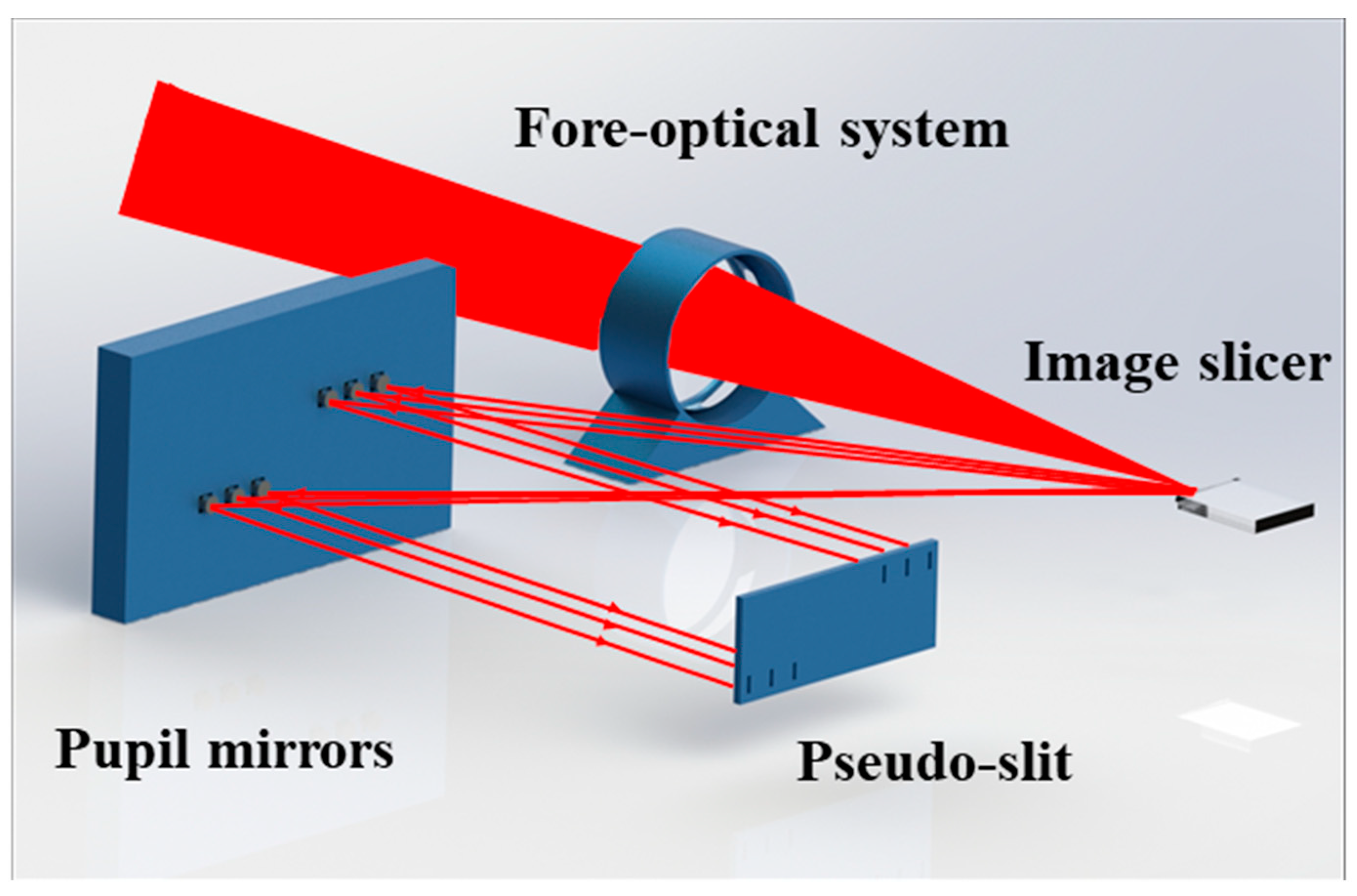
Article

High-Precision Manufacture and Alignment of Image Slicer Based on Thin Glass Bonding

1
MOE Key Laboratory of Advanced Micro-Structured Materials, Shanghai 200092, China
2
Institute of Precision Optical Engineering, School of Physics Science and Engineering, Tongji University, Shanghai 200092, China
3
School of Mechanical Engineering, Tongji University, Shanghai 200092, China
4
Shanghai Astronomical Observatory, Chinese Academy of Sciences, 80 Nandan Road, Shanghai 200030, China
*
Authors to whom correspondence should be addressed.
Appl. Sci. 2023, 13(22), 12170; https://doi.org/10.3390/app132212170
Submission received: 19 September 2023 / Revised: 7 November 2023 / Accepted: 8 November 2023 / Published: 9 November 2023
(This article belongs to the Special Issue Advances in Optical and Optoelectronic Devices and Systems)

Abstract

:
Integral field spectroscopy (IFS) is capable of simultaneously collecting two-dimensional high-resolution spatial image information and spectral information in a target field of view (FOV). The image slicer is the key element in IFS for segmenting the target FOV. Current micro-image slicer fabrication methods such as molecular assembling need strictly accurate control during sticking, which is time-consuming and expensive. In this study, we improved a direct-adhesive method for thin glass slicer manufacture and alignment. Thin glass is fabricated via single polishing and direct stitching to form a micro-image slicer. Based on charge coupled device (CCD) camera tests on parallel light, the manufacture accuracy for a six-channel image slicer reaches that of the molecular assembling scheme. This method can be applied to the fabrication of image slicers with different apertures.

1. Introduction

The integral field spectrometer (IFS) is one of the most important scientific instruments in astronomical research [1,2]. Currently, the main large-aperture astronomical telescopes, such as TMT-IRIS and VLT-MUSE, are equipped with IFSs [3,4,5,6,7], which simultaneously collect both image and spectral information and investigate the physical properties and kinematics within the field of high-resolution two-dimensional (2D) space [8]. The observation time is reduced, and the stability and consistency are improved compared with the conventional 2D imaging spectrometer. The imaging principle of the IFS is shown in Figure 1. The fore-optical system collects the target optical information and images it at the focal plane. An integrated field unit located on the focal plane divides the optical information of the obtained image into several units and rearranges them in the 2D field of view. Then, the light illuminates the slit and enters several dispersive devices in the spectroscope. The required three-dimensional data are obtained through image processing using the spectral information received by the detectors.
As shown in Figure 2, three main techniques are used for the IFS: the micro-lens, micro-lens combined with optical fibers, and image slicer [9,10]. Compared with the IFS using a micro-lens array to segment images, the principle of the image slicer-based IFS is simpler, and the image processing is easier. The utilization ratio of the detector is higher such that almost every pixel of the detector is used. The 2D spatial direction sampling and dispersion direction do not interfere with each other [11]. However, the image slicer is not typically used in IFSs because of its complex structure, large volume, and high cost [12].
Machining and traditional stacking are the two main methods for fabricating image slicers. Machining consists generally in fabricating multi-channel image slicers on a single piece of metal by single-point diamond turning [13,14]. The channel on an image slicer cannot be made too thin because of the limitation of the applicable tools in fabricating individual channels. Moreover, machine manufacturing cannot meet the requirements on surface roughness and shape in the visible light region [15]. This fabrication method is usually applied for large-volume image slicers, such as ground-based telescope infrared integral field spectroscopy slicers, but it is not suitable for small-volume applications. Compared with machining, traditional stacking avoids the difficulty in the fabrication of thinner channels on image slicers. There are two methods for fabricating image slicers by traditional stacking. The first method consists in extracting unique slices from different blank mirrors and stacking all slices together. The second method consists in stacking together multiple eccentricity channels by fabricating all the channels of the image slicer in a single processing. Compared with the former method, the latter is low cost and higher in efficiency [16,17]. The surface accommodates many different fabrication methods to cope with different spectrometer bands. This method can be applied to all types of IFS in different optical systems.
The IFS prototype of the China Space Station Telescope (CCST) specific optical path is shown in Figure 3. Light passes through the fore-optical system and then enters the image slicer at the focal plane. The light is refocused, reflected through pupil mirrors, and enters the spectrometer through a pseudo slit. By folding the optical path, the spectrometer volume is reduced, thereby optimizing the space utilization of the rear end of the telescope. The working wavelength of the spectrometer is 350–1200 nm. The image slicer is manufactured using the second method of traditional stacking. However, this method uses molecular assembling to stack thin glass during the image slicer fabrication. Molecular assembling stacking requires each channel to reach a higher quality for the upper and lower surfaces. To realize molecular assembling, the thin glass slices require extrusion, which deforms the thinner slices. The slicer errors in the bottom layer accumulate on the top surface. The spherical surface made by the molecular assembling of slices differs considerably from the ideal surface after disassembly. In addition, the manufacturing precision of this method is not easily controllable.
In this paper, an improved method is proposed to control the spherical center location of all channels. Each channel of the image slicer is stacked via glue bonding. Errors generated by the different steps are distributed through error decomposition, which confirms the feasibility of glue bonding. Finally, a six-channel high-precision image slicer is made using the proposed method. This method reduces the requirement on the upper and lower surface profiles of the slices and controls the center location on the spherical surface, thereby reducing the manufacturing difficulty and increasing its capability.

2. Design Parameter of Image Slicer

The design parameters of the image slicer are listed in Table 1. The design of the image slicer is based on the eccentricity of the different channels. As shown in Figure 4, the eccentricity of the focus in the final stack of the different channels is realized by controlling the distance between the different slices and the spherical datum plane. The sphere radius R is 340 mm. H is the distance from the bottom surface to the reference surface, and D is the distance from the top surface midcourt line to the reference surface. Up and left define the positive directions. The distance between the spherical surface and reference surface with different slice distances is given in Table 2. Six image slices are stacked together to form an image slicer. The focus for each slice is arranged on a straight line. To minimize the stray light, it is necessary to control the defect of the image slicer unit. Edge defects are controlled within 5 μm via precise polishing on the side of the glass stack block.

3. Image Slicers Fabrication

Classical slices are individually polished. Vives et al. proposed an alternative method to manufacture one or more stacks of slices via a single polishing process [14]. However, their slices are arranged and maintained via molecular assembling, which requires high-precision slice units. To reduce the fabrication difficulties, we propose an improved method, which uses optical glue instead of optical contact. The whole process, shown in Figure 5, is divided into the following five steps: I. rectangular plane slice preparation, II. slice sticking, III. spherical production, IV. image slicer sticking, and V. laser cutting.
I.
Plane rectangular slice preparation
Every slice is made of 0.25 mm thick flat mirrors. The glass slices are cut into different lengths with the same width and height to adapt to different eccentricities. The sizes of the glass slices are shown in Table 3.
II.
Slice sticking
The glass slices of different lengths are stacked to form a block. The gap between the slices is filled with optical glue, and auxiliary blocks are stuck around the block. The auxiliary blocks are two semicircles with the lowest point of the sphere as the center. The entire block is rotated, and the runout of the edges of the auxiliary blocks a and b (shown by the blue line in Figure 5) is measured so that the center of the block coincides with the center of the sphere-making tool. This step allows the center of the sphere to be made faster and more accurately.
III.
Spherical fabrication
A sphere is fabricated on the front side of a block. All slices are produced via a single polishing process.
IV.
Image slicer sticking
The different length slices are stacked in the order of the image slice design, using optics glue. During the stacking process, the spacing layer between the top and bottom groups is removed. The speckles on the top group will fall during the parallel light test.
V.
Laser cutting
A laser is used to cut the excess part of the image slicer.

4. Error Analysis

Errors, induced from the fabrication process, affect the precision of the image slicer. The errors are divided into eccentricity and surface errors. The eccentricity error, including shape, fixture, and stack errors, describes the influence of the final image slice focus location. The surface error involves the surface shape accuracy (peak to valley (Pv)) and surface roughness (profile arithmetic average error (Ra)). The fabrication error of the image slicer is illustrated as an error tree in Figure 6. A summary of error distribution is given in table in Section 4.3.

4.1. Eccentricity Error

Each slice of the surface, used to fabricate the sphere, has a sphere center. Figure 7 specifies the three dimensions that cause the sphere center to be out of position. The first error part is decomposed into the three dimensions.

4.1.1. Shape Error

According to the fabrication process, the shape of the glass slices plays a role in the positioning of the eccentricity degree of the glass slices in the image slicer. Therefore, the shape error is essential to the analysis. Each glass slice is cuboid, and the shape errors are determined by the angle and length. An abridged general view of the slice parameters is given in Figure 8b. The length L determines the displacement in lateral X direction; therefore, the length error L 1 must be precisely controlled. The errors Δ H and Δ W in the height H and width W , respectively, can be removed through polishing the front and back surfaces in the slice sticking process. The errors A 1 , A 2 , A 3 , and A 4 in the angles A 1 , A 2 , A 3 , and A 4 determine the cuboid shape which influences the error control in the stacking process. As shown in Figure 8c,d, different cuboid shapes are affected by the errors A 1 ,   A 2 , A 3 , and A 4 , which cause length measurement error and affect the eccentricity degree in the X direction. The relationship between the error factors and influence quantities is listed in Table 4.

4.1.2. Fixture Error

The accuracy of the fixture for the installation of the glass slices affects the stack accuracy, which determines the eccentricity of the focus. The precision of the angles between surfaces S 1 , S 2 , and S 3 , including the surfaces morphology, determine the precision of the stack. The P v of surfaces S 1 , S 2 , and S 3 need to be controlled under 0.5 μm. The errors A 5 , A 6 , and A 7 in the angles A 5 , A 6 , and A 7 , shown in Figure 9b, result in the tilting of all slices, which leads to the eccentricity of the X- and Y-axes. In the ideal condition, A 6 is 90° and A 6 is 0°, i.e., the right side of the slices is in contact with surface S 2 . When A 6 is non-zero, the slice is firstly in contact with S 1 and moves to S 2 along the boundary of S 1 to make a line contact with S 2 . Due to the geometrical limitation of the S 1 S 2 boundary, the slices can be aligned within the same XZ position; hence, the tilt effect caused by the error A 6 can be ignored. The relationship between the error factors and influence quantities is listed in Table 5. The error diagram is given in Figure 9 with the different error angles.
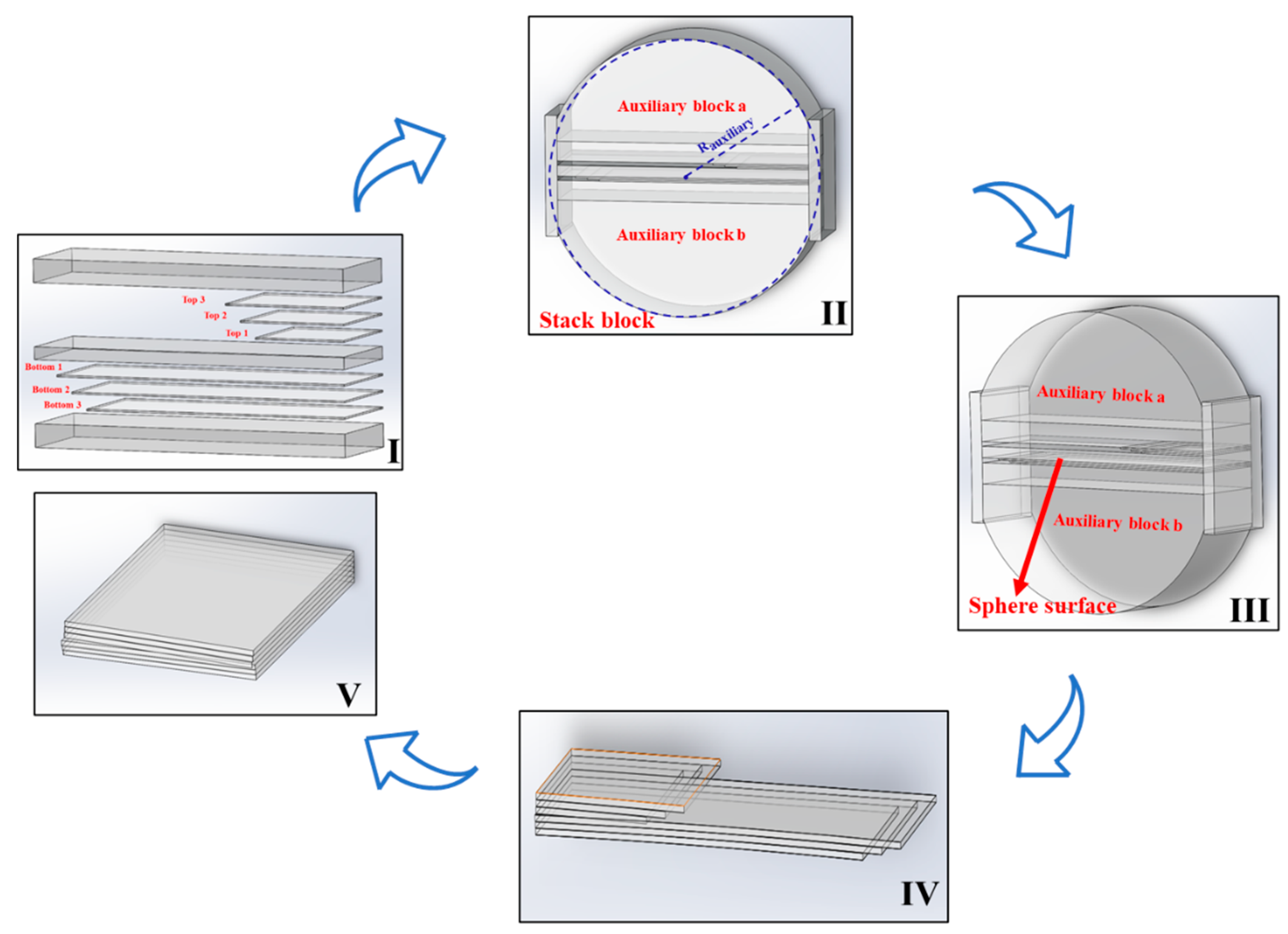
4.1.3. Stack Error

Stacking error is introduced during the slice and image slicer sticking processes (Section 3, processes II and IV). The accuracy of the double stacking process affects the final image slicer accuracy. By analyzing the stacking error, we can improve the sensitivity of the error analysis and ensure better manufacturing through accuracy allocation.
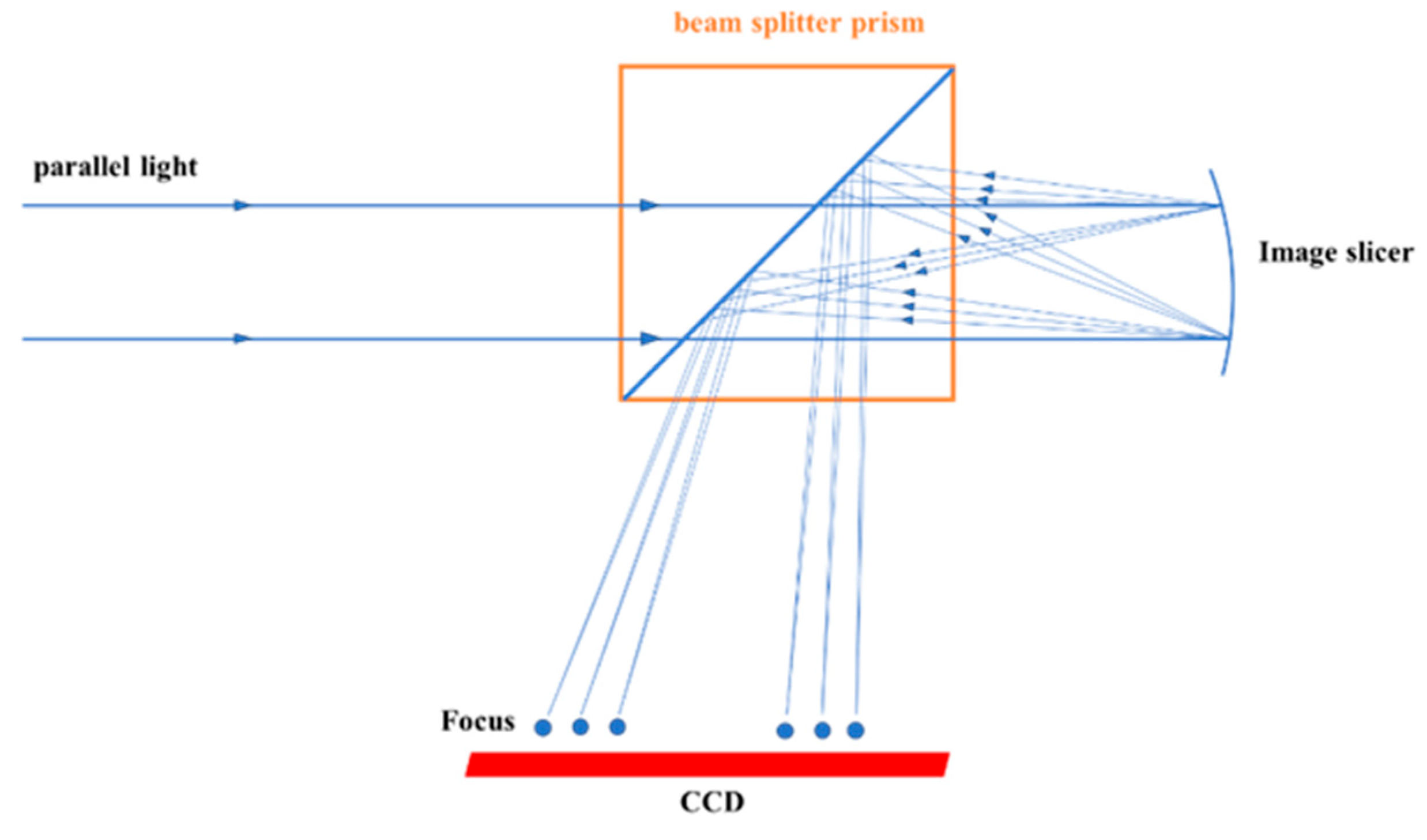
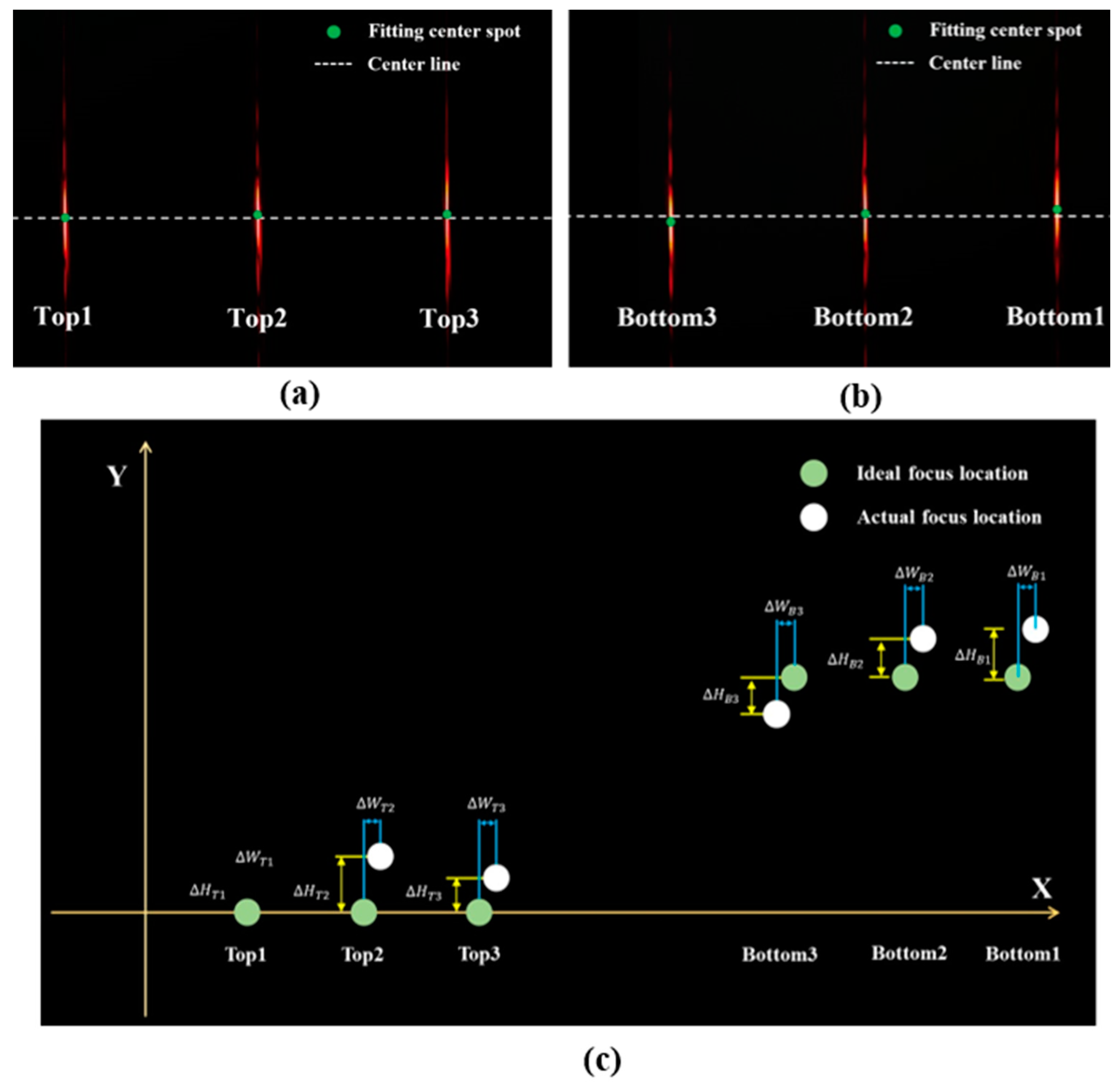
The errors of the stack are divided into translation error and rotation error. We define the ideal position ( X n , Y n , Z n ) of each slice at sphere fabrication as the origin. A shift in the XYZ direction directly affects the XYZ eccentricity, whose corresponding error values are X n , Y n , Z n . The combination of the rotation error caused by the thickness of the adhesive layer complicates XYZ eccentricity. In the following discussion, the rotation error is divided into pitch, yaw, and roll errors which are analyzed separately.
The errors in pitch, yaw, and roll affect the errors of the YZ, XZ, and XY eccentricities, respectively. The effect of the YZ eccentricity error, caused by the pitch angle, can be analyzed by axial translation and rotation. The pitch error is divided into two situations: slice working surface contact, shown in Figure 10a, and slice back surface contact, shown in Figure 10b. The contact pitch errors for both cases are shown in Figure 10c,d. In Figure 10c, n H represents the n th channel of the image slicer. The pitch error can be analyzed by translation and rotation. The behavior of the channel slice with pitch error can be obtained by rotating the ideal channel slice around the X-axis on the sphere center. The distance translation between the rotational and actual positions is the translation error in the XZ direction. Using the same method, we can obtain the translation error for the slice back surface contact, as shown in Figure 10d. The auxiliary angle θ t 8 is given by:
θ t 8 = sin 1 n H R
The angle error A 8 of the pitch results in the eccentricity errors Y 8 and Z 8 at the Y and Z direction. For the slice working surface contact (Side 1 contact, Side 2 separate), the Y eccentricity error Y 8 1 is given by:
Y 8 1 = R sin A 8 1 + θ t 8 n H R A 8 1
The Z eccentricity error Z 8 1 should satisfy
Z 8 1 = R cos A 8 1 + θ t 8 cos θ t 8 Y 8 1
For the slice back surface contact (Side 2 contact, Side 1 separate), the error value can be obtained by translating the above situation. The Y eccentricity error Y 8 2 is given by:
Y 8 2 = R sin A 8 2 + θ t 8 + W sin A 8 2 n H R A 8 2
The Z eccentricity error Z 8 2 satisfies
Z 8 2 = R cos A 8 2 + θ t 8 cos θ t 8 + W 1 cos A 8 2 Y 8 2
The effect of the XZ eccentricity error, caused by the yaw angle, can be analyzed by axial translation and rotation. An abridged general view of the yaw error is given in Figure 11a. The error analysis process is illustrated in Figure 11b. The slicer rotates from the ideal position to the rotational position around the Y-axis. The sphere center remains unchanged. The XZ direction displacement of the slicer from the rotational position to the actual position constitutes the eccentricity error in the XZ direction. The auxiliary angle θ t 9 used to analyze this error satisfies
θ t 9 = tan 1 D + L 2 R 2 n H 2 + W + Δ A 9
The angle error A 9 of the pitch, causing the X eccentricity error X 9 and Z eccentricity error Z 9 , is given by the formula. The X eccentricity error X 9 is given by:
X 9 = R 2 n H 2 + W 2 + D + L 2 2 sin θ t 9 L cos Δ A 9 D L 2 R Δ A 9
The Z eccentricity error Z 9 should satisfy
Z 9 = R 2 n H 2 + W sin Δ A 9 R 2 n H 2 + W 2 + D + L 2 2 cos θ t 9 X 9
The effect of the XY eccentricity error, caused by the roll angle, can be analyzed by axial translation and rotation. An abridged general view of the roll error is given in Figure 12. The auxiliary angle θ t 9 used to analyze this error satisfies
θ t 10 = tan 1 D L 2 n H
The angle error A 10 of the pitch, causing the X and Y eccentricity errors X 10 and Y 10 , respectively, is given by Equation (10). The X eccentricity error X 10 should satisfy
X 10 = n H sin A 10 θ t 10 cos θ t 10 + n H tan θ t 10
The Y eccentricity error Y 10 should satisfy
Y 10 = n H 1 cos A 10 θ t 10 cos θ t 10
The thickness of each layer slice glue line, affecting the Y-axis eccentricity including all subsequent slices, needs to be taken into account. The thickness of glue line Y 2 causes the error Y 2 . The main influence quantity of the pitch, yaw, and roll is given in Table 6. Other errors are fully eliminated if the listed eccentricity errors are removed.

4.2. Surface Error

The shape error is the height mismatch between the image slice and ideal spherical surface. The image slice deformation during stacking results in changes in the surface shape, which can be monitored using a 4D interferometer. As the shape error causes speckle change during the focusing process, controls of less than 40 nm on the surface shape RMS of each slice sphere are needed during stacking. In addition, the surface roughness R a should be less than 2 nm to reduce scattering.

4.3. Summarize Error

Appropriate adjustment on the tolerance can reduce the manufacturing difficulty as the error sensitivity varies. Through the above analysis, the error distribution is performed according to different error sensitivities. The eccentricity error of each slice in the X Y Z direction should be less than 20 μm in the last image slices. The distribution of errors is elaborated in Table 7.

5. Fabrication of Image Slicers

The image slicer is fabricated from 0.25 mm SCHOTT D263 thin glass, glued by LOCTITE GLUE 417. As shown in Figure 13a, the thin glass stacking fixture consists of a 6061-aluminum plate and two prisms. K9 glass plate surface precision P V < 1 / 10 λ   ( λ = 632.8   n m ) . Every angle of prism is under 10″, which means the actual precision can meet the precision requirement of the stack fixture. Different length thin glass slicers are shown in Figure 13b. The alignment process of the thin glasses with stack fixtures is shown in Figure 13c, which is the stack process before sphere production. The sphere has been fabricated on the surface of a stack block, which is shown in Figure 13d. Every channel has been stripped from the stack block after heating, which is shown in Figure 13e. Finally, as shown in Figure 13f, all channels of image slicers are aligned on the left in order, which must obey the same order as the original stacking. The image slicer is removed from the stacking fixture and the excess part is cut away with the inside diameter slicer.

6. Measurement

6.1. Test Method

Parallel light is used for the image slicer error detection. Parallel light illuminates first a beam splitter prism and then the image slicer. The light from the image slicer is then reflected by the prism and finally focused on a CCD detector to measure the distance between the focus of each two image slices. According to the design, the distance between the focus of each two image slices is 2 mm. The measurement optical path is shown in Figure 14. The actual structure of the optical system is shown in Figure 15. A 4D interferometer laser is used as a parallel light source. The pixel size of the CCD is 2.4 μm, which means the CCD meets the test requirements. The CCD is placed on a closed-loop control, high-precision, five-dimensional adjustment frame with XYZ movement accuracy of 0.002 mm. The distance beyond the measurement range of a CCD single frame is measured using the five-dimensional adjustment frame.
Surface error and roughness will be measured using a 4D interferometer and white light interferometer.

6.2. Test Result

The distance between the two focuses in the X direction is 2 mm. The permissible eccentricity error is 20 μm. The focus of the image slicer in the XY direction is shown in Figure 16a,b (light bars). The actual and ideal positions of the focal point are shown in Figure 16c. The XY-axis distances for the different channels are detailed in Table 8. The focus of bottom 3 exceeds the range allowed by the ideal focus position. It is found that the yaw error in the last stacking process is caused by the accumulation of the LOCTITE glue. It will be necessary to modify the fixture in future stacking processes to prevent the glue from accumulating. The Z-axis offset is obtained by detecting the exposure on a CCD mounted on a five-dimensional adjusting frame. The distance between the maximum exposure of the different channels and the first channel is measured by adjusting frame calibration. The final location errors we measured are less than 0.01 mm compared with 0.02 mm of the initial design. To reduce the effect of the location error, pupil mirrors are appropriately adjusted, thereby allowing the reflected light to enter the slit.
The surface accuracy RMS of each slice was evaluated using a 4D interferometer, and it was found to be better than 1/60 λ ( λ = 632.8   n m ). The surface accuracy RMS falls significantly below the specified tolerance of 40 nm. The roughness was measured using a Bruker white light interferometer, with a 50× objective lens and 1× eyepiece. The obtained roughness R a is less than 1 nm. Detailed data for each slice are presented in Table 9. The excellent surface accuracy and roughness achieved demonstrate the inherent benefits of traditional polishing techniques. The lower surface shape accuracy simultaneously demonstrates superior stress control during the glue bonding process, thereby preventing deformation in the working area of the image slicer.

7. Conclusions

This paper classifies and summarizes the fabrication process of the image slicer by previous scholars. The simultaneous manufacturing of all the image slicer channels by moving the glass sheet of different lengths is described. An improvement in the determination of the center of a sphere manufactured using an auxiliary block is given. Instead of molecular assembling, glue assembling is adopted for stacking to reduce the quality requirement between the upper and lower surfaces of the glass sheet, thereby reducing the production difficulty. The fabrication error tolerances are analyzed by distinguishing eccentricity and shape errors to reduce the precision requirement. The error distribution is performed according to the fabrication difficulty in different processes. Parallel light was used to test the image slicer fabricated using the method above. The focus spacing of each channel meets the requirements in the X and Y direction except for one channel that exceeds the requirement in the X direction. The X direction error of BOTTOM3 is 31.2 μm, which exceeds the requirement of 20 μm. The distance error is converted into an angle error of 18 arcsec. This error still falls below the requirement of 20 arcsec for ground-based IFS prototypes (VLT second-generation instruments) [18]. The manufacturing method holds significant importance in the IFS prototyping of CCST. By controlling the focus position during glue curing, this scheme is likely to produce a qualified image slicer.

Author Contributions

Methodology, P.C.; formal analysis, P.C.; investigation, P.C. and Z.S.; writing—original draft, P.C.; writing—review and editing, P.C. and J.X.; supervision, J.Y., K.L. and Z.S.; project administration, Z.W.; funding acquisition, Z.S. and K.L. All authors have read and agreed to the published version of the manuscript.

Funding

This work was supported by the National Natural Science Foundation of China (No. 12373100), the Interdisciplinary Project in Ocean Research of Tongji University, and the Shanghai Astronomical Observatory, Chinese Academy of Sciences.

Institutional Review Board Statement

Not applicable.

Informed Consent Statement

Not applicable.

Data Availability Statement

Data are contained within the article.

Conflicts of Interest

The authors declare no conflict of interest.

References

  1. Content, R.; de Ugarte Postigo, A.; Thöne, C.; Sheinis, A. The Advanced Image Slicers of OCTOCAM. Adv. Opt. Mech. Technol. Telesc. Instrum. III 2018, 10706, 1861–1869. [Google Scholar]
  2. Dubbeldam, C.M.; Robertson, D.J.; Rolt, S.; Talbot, R.G. An Alternative Design for a Metal Image Slicing IFU for EAGLE. Mod. Technol. Space-Ground-Based Telesc. Instrum. II 2012, 8450, 1471–1480. [Google Scholar]
  3. Tsuzuki, T.; Ozaki, S.; Miyazaki, S.; Fucik, J. Image Slicer Module for Wide Field Optical Spectrograph (WFOS). Ground-Based Airborne Instrum. Astron. VII 2018, 10702, 2653–2659. [Google Scholar]
  4. Ozaki, S. Design Study of an Image Slicer Module for a Multiobject Spectrograph. J. Astron. Telesc. Instrum. Syst. 2019, 5, 035001. [Google Scholar] [CrossRef]
  5. Henault, F.; Bacon, R.; Content, R.; Lantz, B.; Laurent, F.; Lemonnier, J.-P.; Morris, S.L. Slicing the Universe at Affordable Cost: The Quest for the MUSE Image Slicer. Opt. Des. Eng. 2004, 5249, 134–135. [Google Scholar]
  6. Zhang, K.; Zhou, Y.; Moore, A.M.; Chisholm, E.M.; Larkin, J.E.; Wright, S.A.; Zhu, Y.; Hu, Z.; Reiley, D.J. The Infrared Imaging Spectrograph (IRIS) for TMT: Design of Image Slicer. Ground-Based Airborne Instrum. Astron. VII 2018, 10702, 2904–2916. [Google Scholar]
  7. Avila, G.; Guirao, C.; Baader, T. High Efficiency Inexpensive 2-Slices Image Slicers. Ground-Based Airborne Instrum. Astron. IV 2012, 8446, 1444–1449. [Google Scholar]
  8. Kushibiki, K.; Hosobata, T.; Takeda, M.; Yamagata, Y.; Morita, S.; Motohara, K.; Ozaki, S.; Tsuzuki, T.; Takahashi, H.; Kono, Y.; et al. Fabrication of Mirror Arrays with an Ultra-Precision Cutting Technique for a near-Infrared Integral Field Unit SWIMS-IFU. Adv. Opt. Mech. Technol. Telesc. Instrum. IV 2020, 11451, 149. [Google Scholar]
  9. Dubbeldam, C.M.; Content, R.; Allington-Smith, J.R.; Pokrovski, S.; Robertson, D.J. Integral Field Unit for the Gemini Near-Infrared Spectrograph. Opt. IR Telesc. Instrum. Detect. 2000, 4008, 1181–1192. [Google Scholar]
  10. Sharples, R.M.; Allington-Smith, J.R.; Buscher, D.F.; Content, R.; Haynes, R.; Myers, R.M. Recent Developments in Spectroscopy. New Astron. Rev. 2001, 45, 77–81. [Google Scholar] [CrossRef]
  11. Allington-Smith, J. Integral Field Spectroscopy for Panoramic Telescopes. Rev. Mex. Astron. Astrofísica 2007, 28, 17–23. [Google Scholar]
  12. Doolan, M.C.; Dopita, M.A.; Waldron, L.E.; Hart, J.; Zhelem, R.; Bloxham, G.; Conroy, P.; McGregor, P.; Pfitzner, L. Optical Wavelength Image Slicer. Ground-Based Instrum. Astron. 2004, 5492, 421–428. [Google Scholar]
  13. Cuevas, S.; Eikenberry, S.S.; Sánchez, B. FRIDA Integral Field Unit Manufacturing. Adv. Opt. Mech. Technol. Telesc. Instrum. 2014, 91514, 1573–1580. [Google Scholar]
  14. Vives, S.; Prieto, E.; Salaun, Y.; Godefroy, P. New Technological Developments in Integral Field Spectroscopy. Adv. Opt. Mech. Technol. Telesc. Instrum. 2008, 7018, 959–968. [Google Scholar]
  15. Dubbeldam, C.M.; Robertson, D.J.; Preuss, W. Freeform Diamond Machining of Complex Monolithic Metal Optics for Integral Field Systems. Opt. Fabr. Metrol. Mater. Adv. Telesc. 2004, 5494, 163–175. [Google Scholar]
  16. Renault, E.; Laurent, F.; Kosmalski, J.; Adjali, L. CRAL Expertise on Image Slicer: Optical Designs, Glass or Metallic Manufacturing, Test and Results. Adv. Opt. Mech. Technol. Telesc. Instrum. 2008, 7018, 880–891. [Google Scholar]
  17. Prieto, E.; Vivès, S. Low-Cost Multi-Integral Field Unit (IFU) with High-Quality Optical Polishing. Optomech. Technol. Astron. 2006, 6273, 534–543. [Google Scholar]
  18. Bonneville, C.; Prieto, E.; Ferruit, P.; Henault, F.; Lemonnier, J.-P.; Prost, F.; Bacon, R.; Le Fevre, O. Design, prototypes, and performance of an image slicer system for integral field spectroscopy. Astron. Telesc. Instrum. 2003, 4842, 162–173. [Google Scholar]
Figure 1. Principle diagram of integral field spectrometer.
Applsci 13 12170 g001
Figure 2. A summary of three main techniques for integral field spectrograph [10].
Applsci 13 12170 g002
Figure 3. Schematic of the optics system design.
Applsci 13 12170 g003
Figure 4. Schematic of the image slicer design. The distance between image slicer surface and fitting spherical.
Applsci 13 12170 g004
Figure 5. Process of image slicer fabrication. The fabrication process is divided into five steps: plane rectangular slices preparation, slice sticking, spherical fabrication, image slicer sticking, and laser cutting.
Applsci 13 12170 g005
Figure 6. Error tree of image slicer fabrication. The errors produced in the fabricating process are classified into four kinds: length error, fixture error, stack error, and surface error.
Applsci 13 12170 g006
Figure 7. Three dimensions of the sphere to be out of position.
Applsci 13 12170 g007
Figure 8. Error decomposition diagram: (a) ideal long thin glass slicer; (b) different parameters on the thin glass slice; (c) A 1 ,   A 2 error schematic diagram in top view of the thin glass; (d)   A 3 error schematic diagram in side view of the thin glass.
Applsci 13 12170 g008
Figure 9. Error decomposition diagram: (a) ideal frock fixture; (b) different parameters on frock fixture; (c) A 5 error schematic diagram in XY view of thin glass; (d)   A 7 error schematic diagram in YZ view of thin glass.
Applsci 13 12170 g009
Figure 10. Different contact situation of pitch error: (a) A schematic diagram of the first situation of pitch error. (b) A schematic diagram of the second situation of pitch error. (c) Schematic diagram of the first situation of pitch error analysis. The slicer rotates from ideal position to rotational position and then translates to translation position. (d) Schematic diagram of the second situation of pitch error analysis. The slicer rotates and translates from ideal position to translation position based on the first situation. Then, the slicer translates from translation to actual position.
Applsci 13 12170 g010
Figure 11. Yaw error of stack in the top view: (a) A schematic diagram of the yaw error. (b) Schematic diagram of the yaw error analysis. The slicer rotates from ideal position to rotational position around Z-axis and then translates to translation position.
Applsci 13 12170 g011
Figure 12. Error decomposition diagram: (a) roll error of stack in the front view; (b) calculation error by analyzing axial translation and rotation.
Applsci 13 12170 g012
Figure 13. Practical fabrication process: (a) the stack fixture consists of two high-precision orthogonal prisms; (b) thin glass of different length; (c) using the stack fixture aligns different length thin glass on the right side; (d) the auxiliary blocks are bonded on the top and bottom of stack block; (e) the sphere is produced on the front side of glass slice; (f) using the stack fixture aligns different length thin glass on the left side.
Applsci 13 12170 g013
Figure 14. Schematic of optical system detection. The parallel light incident into the image slicer is focused on the CCD side by means of a splitter prism.
Applsci 13 12170 g014
Figure 15. The detection optical system of image slicer focus.
Applsci 13 12170 g015
Figure 16. Test result diagram: (a) the focus test result of the top three channels and the fitting center spots are marked on the figure; (b) the focus test result of bottom three channels and the fitting center spots are marked on the figure; (c) the schematic of different channel focus.
Applsci 13 12170 g016
Table 1. Summarized parameters of image slicer.
TypeField Angle/Arcsec Size / mm   ( w × l × h )
Single slice field 0.2 × 0.2 12 × 9 × 0.25
Image slicer field 1.2 × 1.2 12 × 9 × 1.5
Table 2. Location of different channels in fitting spherical.
ChannelDistance H (mm)Distance D (mm)
Top 32.25−9.5
Top 22.00−11.5
Top 11.75−13.5
Bottom 1−0.2513.5
Bottom 2−0.5011.5
Bottom 3−0.759.5
Table 3. Length of single thin glass in different channels.
Length (mm)Width (mm)Height (mm)Location
12130.25Top 1
14130.25Top 2
16130.25Top 3
35130.25Bottom 3
37130.25Bottom 2
39130.25Bottom 1
42133.25Assist layer
42131.75Assist layer
42133.25Assist layer
Table 4. A summary of length errors for X eccentricity influence.
Slice ParameterErrorInfluence Quantity
L L 1 L 1
A 1 A 1 W × t a n A 1
A 2 A 2 W × t a n A 2
A 3 A 3 H × t a n A 3
A 4 A 4 H × t a n A 4
Table 5. A summary of fixture error.
Slice ParameterErrorInfluence
S 1 P v 1 Z eccentricity
S 2 P v 2 X eccentricity
S 3 P v 3 Z eccentricity
A 5 A 5 X eccentricity
A 7 A 7 Z eccentricity
Table 6. A summary of stack error.
Slice ParameterErrorInfluenceInfluence Quantity
X 1 X 1 X eccentricity X 1
Y 1 Y 1 Y eccentricity Y 1
Z 1 Z 1 Z eccentricity Z 1
A 8 A 8 Y eccentricity A 8 R
A 9 A 9 X eccentricity Δ A 9 R
A 10 A 10 Y eccentricity n H A 10
Y 2 Y 2 Y eccentricity Y 2
Table 7. Summary of error in image slices fabrication.
Error InfluenceError Influence ItemErrorError RequirementError QualityCumulative Error
Eccentricity errorX eccentricity L 1 1 μm1 μm20 μm
A 1 22.9″1 μm
A 2 22.9″1 μm
A 3 13.7′1 μm
A 4 13.7′1 μm
P v 2 0.5 μm0.5 μm
A 5 13.7′1 μm
X 1 1 μm1 μm
A 9 7.5″12.5 μm
Y eccentricity Y 1 1 μm1 μm20 μm
A 8 10.6″17.5 μm
A 10 8.6′1 μm
Y 2 0.5 μm0.5 μm
Z eccentricity P v 1 0.5 μm1 μm4 μm
P v 3 0.5 μm1 μm
A 7 13.7′1 μm
Z 1 1 μm1 μm
Surface errorRMS40 nm40 nm40 nm
Ra2 nm2 nm2 nm
Table 8. The value of X-axis error and Y-axis error.
Channel NumberDistance Error (mm)Channel NumberDistance Error (mm)
W T 1 0 H T 1 0.0000
W T 2 0.0144 H T 2 0.0096
W T 3 0.0072 H T 3 0.0024
W B 3 0.0312 H B 3 0.0048
W B 2 0.0192 H B 2 0.0072
W B 1 0.0048 H B 1 0.0168
Table 9. The surface shape accuracy and roughness values of different slices.
Slice Number Surface   Accuracy   ( λ ) Roughness (nm)
Top 10.00600.900
Top 20.00570.583
Top 30.00460.685
Bottom 10.00640.565
Bottom 20.00490.524
Bottom 30.00480.647
Disclaimer/Publisher’s Note: The statements, opinions and data contained in all publications are solely those of the individual author(s) and contributor(s) and not of MDPI and/or the editor(s). MDPI and/or the editor(s) disclaim responsibility for any injury to people or property resulting from any ideas, methods, instructions or products referred to in the content.

