
O-Band Grating Couplers Using Silicon Nitride Structures

Faculty of Engineering, Holon Institute of Technology (HIT), Holon 5810201, Israel
*
Author to whom correspondence should be addressed.
Appl. Sci. 2023, 13(17), 9951; https://doi.org/10.3390/app13179951
Submission received: 22 July 2023
/
Revised: 9 August 2023
/
Accepted: 27 August 2023
/
Published: 3 September 2023
(This article belongs to the Special Issue Waveguide Technology: Development and Applications)
Abstract
:To test silicon photonics component performances, a silicon (Si) grating coupler (GC) is used to couple the light from a single-mode fiber (SMF) into the chip. However, silicon nitride (Si3N4) waveguides have recently become more popular for realizing photonic integrated circuits (PICs), which may be attributable to their exceptional characteristics, such as minimal absorption and low back reflection (BR) in the O-band spectrum. Thus, to test the photonic chip, a waveguide converter from Si3N4 to Si needs to be added to the photonic circuit, which can lead to more power losses and BR. To avoid this conversion, we propose in this manuscript a configuration of a GC based on Si3N4 structures, which can be employed to minimize the footprint size and obtain better performance. The achievement of high efficiency was possibly obtained by optimizing the structural properties of the waveguide and the coupling angle from the SMF. The results demonstrated high efficiency within the O-band spectrum by using a wavelength of 1310 nm. Notably, at this specific wavelength, the findings indicated a coupling efficiency of −5.52 db. The proposed design of the GC consists of a uniform grating that offers improvements regarding affordability and simplicity in manufacturing compared to other GC models. For instance, using a reflector or a GC with non-uniform grooved teeth introduces challenges in fabrication and incurs higher costs. Thus, the proposed design can be useful for improving the testing abilities of the Si3N4 photonic chips used in transceiver systems.
1. Introduction
Grating couplers (GC) based on silicon (Si3N4) are now widely used to couple the light between a single-mode fiber (SMF) and photonic integrated circuits (PICs) [1,2]. The use of GC in the field of PICs has brought significant advantages by enabling the avoidance of expensive processing and packaging steps [3]. GCs are devices that couple light into and out of waveguides on PICs [4,5]. They supply a proficient and budget-friendly resolution, achieving an efficient interface between the optical fiber and waveguides on the PICs without the need for complex alignment techniques [6,7,8]. Traditionally, the optical waveguides on chips required polishing to achieve good coupling efficiency with optical fibers [9]. This process was time-consuming and costly, as it involved the precise polishing and alignment of the waveguide facets [10]. Similarly, lensed fibers were used to focus light into the waveguides, which required careful alignment and often resulted in additional expenses [11,12]. GCs can be useful in addressing this challenge by enabling efficient optical signal coupling and transmission [13]. A GC based on Si3N4 has become a preferred choice for PICs because of its excellent optical properties, such as low absorption and low back reflection (BR) in the O-band spectrum [14,15,16]. These properties are crucial in integrated photonic systems as they help prevent signal degradation, interference, and increased noise levels, ensuring high-quality and efficient signal transmission [17]. A study [18] was conducted by employing an Si3N4 on a silicon (Si) bi-layer configuration. This O-band design was developed through an optimization-driven strategy and realized on a 200 mm wafer. These designs exhibited resilience to fabrication variations, maintaining a consistently high performance across the entire wafer. Particularly noteworthy is the attainment of a remarkable peak coupling efficiency of −2.2 dB and a substantial 1-dB wavelength range of 72.9 nm in a representative device. Additionally, an innovative accomplishment is presented in a study [19], introducing a trim Sin platform that enables a fiber-chip featuring a dual-band grating coupler with single-state polarization in the transverse electric (TE) mode. This coupler efficiently couples with both O- and C-band wavelengths. In the field of photonics, testing the performance of photonic chips is a crucial step in the development and characterization of integrated photonic devices [20]. A study [21] proposed a design optimization approach to enhance the efficiency of GC using Si material. The focus of their work was to improve the coupling efficiency by utilizing Si on insulator (SOI) technology, which involved a top Si layer with a buried oxide layer. The GC was designed to operate in the TE mode. The result of this study was 30% coupling efficiency with a 1 dB bandwidth of 40 nm on standard wafers. Another study [22] aimed to address the bandwidth limitation of GC. The researchers proposed a focusing-curved arrangement utilizing wide band subwavelength grating couplers (SWGCs). The SWGCs are created using electron-beam lithography (EBL) on a conventional SOI platform through a one-stage complete etching process. TE mode light demonstrates a 1 dB bandwidth exceeding 100 nm around the 1550 nm wavelength. This proposed solution enables seamless integration with different optical devices and systems, expanding the capabilities of GC. An additional notable study [23] delves into the application of Si3N4 as a waveguide. This study demonstrates a semiconductor laser’s functionality within a structured Si photonics platform, displaying proficient light coupling into a waveguide. The diode laser employed in this research is centered on mid-infrared gallium antimonide, grown directly on a pre-patterned Si photonics wafer featuring Si3N4 waveguides enveloped by Si dioxide. The experimental outcomes are striking, as the laser emits over 10 mW of continuous wave light at room temperature. Impressively, approximately 10% of this light is effectively directed into the Si3N4 waveguides. This accomplishment highlights the potential of Si3N4 waveguides as a viable stage for integrating semiconductor lasers on a chip, promising significant advancements in integrated photonics technology. When used for testing Si3N4 waveguide signals within a photonic chip, the use of a waveguide converter from Si3N4 to Si can decrease the performance due to a few factors [24,25]. The difference in the refractive index between Si3N4 and Si can cause mode mismatch and lead to increased coupling losses during the transition [26,27]. Additionally, the fabrication process and material properties of the waveguide converter can introduce additional losses, such as scattering or absorption, which can further degrade the overall performance [28]. Furthermore, the interface between the Si3N4 waveguide and Si waveguide converter may introduce reflections or mode distortions, affecting signal integrity and transmission efficiency. During the conversion, there is the potential for BR in the system and power degradation, which can affect the accuracy and reliability of the testing results. The need for a waveguide converter from Si3N4 to Si can result in the increased footprint size of the photonic chip. The additional space required for integrating the converter adds complexity and potentially limits the available area for other components or functionalities on the chip. One popular waveguide converter is the mode-size converter [29], which is a device that converts the size of optical waveguide modes. An example of a high-efficiency, wideband fiber-to-waveguide mode-size converter with minimal coupling loss has been validated on nano-scale waveguides on the SOI platform [30]. In this mode-size converter, the goal is to efficiently couple light into a conventional single-mode fiber (SMF) possessing a mode field diameter (MFD) of approximately 9.6 µm to the nano-scale waveguides with smaller MFD, typically around 500 nm or less [31,32,33]. The challenges associated with this mode-size converter include the significant mode mismatch between the larger MFD of the SMF and the smaller MFD of the nano-scale waveguide [34,35]. This mode mismatch leads to high coupling losses, limiting the efficiency and performance of the converter. To address the challenges mentioned earlier, we propose a GC using Si3N4 on an insulator substrate that operates within the O-band spectrum under a TE polarization mode. The geometric parameters critical for optimal performance were fine-tuned using the finite difference time domain (FDTD) technique to achieve power distribution, modal analysis, and design optimization. This study shows the ability to design an excellent Si3N4 GC with high light efficiency in the O-band spectrum, which can be very useful for testing Si3N4 photonic chips in data center applications.
2. Grating Coupler Design and Theoretical Aspects
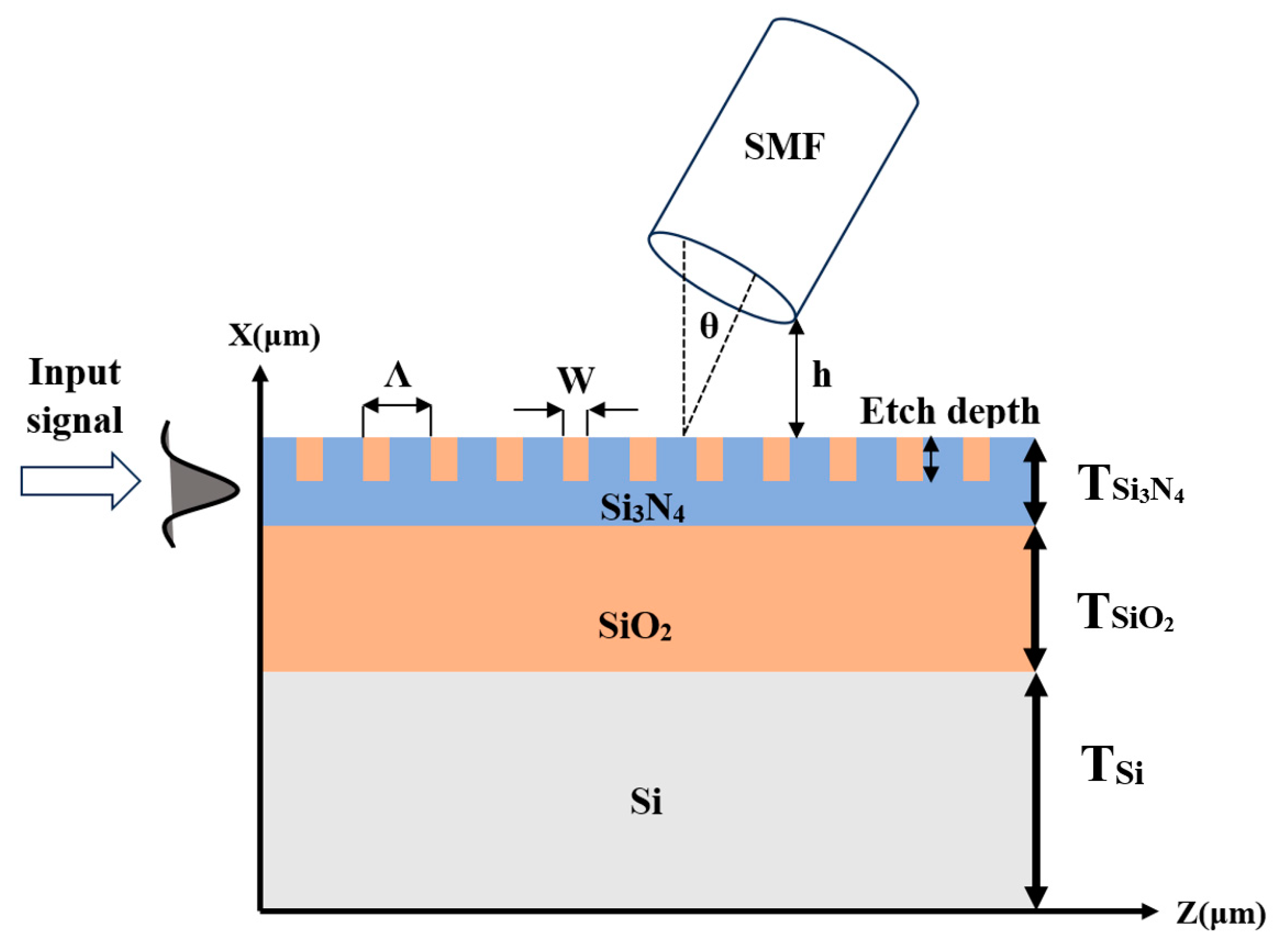
Figure 1 provides a detailed representation of the x-z cross-section structure of the GC waveguide with the SMF, highlighting its key geometrical parameters.
In our model, we selected the GC based on a uniformly grooved teeth configuration for its ease of fabrication and compact footprint, which leads to low-cost GC devices. It is important to emphasize that while complex configurations, such as using a reflector [35,36], a GC with non-uniform grooved teeth [37,38,39,40,41,42], or edge couplers [38], can improve coupling efficiency, they also introduce fabrication difficulties and increased costs. For example, the reflectors used in GCs are sensitive to fabrication variations, such as dimensional errors or imperfections in the grating structure. Similarly, non-uniform grooved teeth increase the complexity of the fabrication process, making precise control over the grating structure and dimensions more challenging. Even small fabrication variations can significantly impact device performance. Due to these considerations, the design of a GC with a uniformly grooved teeth configuration is a reliable, easy-to-fabricate, and cost-effective choice.
Our proposed design consists of three layers with different thicknesses that are carefully chosen to achieve maximum coupling efficiency between the GC and SMF at a wavelength of 1310 nm. The sub-ground layer is made of Si (TSi) with a thickness of 4 μm, followed by a middle layer of SiO2 with a thickness of 1 μm. The top layer is composed of Si3N4 (TSi3N4) with a thickness of 0.76 μm. The top layer features grooved teeth made of SiO2 material. The grating period between the grooved teeth, denoted as Λ, has been set to 0.84 μm, where the SiO2 width of each grooved tooth is 0.34 μm, represented by W, and the Si3N4 width of each grooved tooth is 0.5 μm. The angle of the SMF, defined as θ, is 7.5 degrees, and the distance between the SMF and GC, denoted as h, is 2.6 μm. The etch depth corresponds to the thickness of the grooved teeth, and the optimal value for this parameter is 0.38 μm. By optimizing these key values, the light can propagate through the GC more effectively, and as a result, achieve higher light coupling efficiency between the GC and SMF.
To analyze the propagation characteristics of light within the GC waveguide, we employed the FDTD method. This numerical technique provides valuable insights into the behavior of electromagnetic fields and their propagation through the GC waveguide.
The principal work of GC is to change the mode size of the Si3N4 waveguide to be a better match to the SMF mode. Mode matching refers to ensuring that the guided mode in the Si3N4 waveguide is appropriately coupled to the desired SMF mode for efficient light transmission. To achieve this goal, the Bragg condition [1] must be fulfilled, which can be achieved by carefully optimizing the grating parameters, such as the grating period, the coupling angle from the SMF, and etch depth, and the GC can enhance the coupling efficiency, enabling the effective transmission of light into and out of the Si3N4 waveguide.
The grating period Λ is the key parameter that refers to the distance between the grooves in the grating structure. The grating period Λ of the GC is given by [21]:
Within this mathematical expression, λ symbolizes the wavelength, neff is the refractive index, nc is the refractive index of the cladding material, and θ is the coupling angle from the SMF.
The diffraction behavior of a GC can be described using the Bragg condition, which is also referred to as the phase matching condition. This reveals the relationship between the wave-vector k0 of a light beam through the waveguide and propagation constant β of the corresponding coupled light beam out of the waveguide to the SMF, and the Bragg condition is expressed as [1]:
where denotes the grating vector, while m corresponds to the order of grating diffraction.
To calculate the coupling efficiency between the modes of the waveguide and SMF, we need to calculate the overlap integral between the Gaussian profile of the waveguide and the Gaussian profile of the SMF [21].
This equation is for two-dimensional and TE polarization, and α(z) is the coupling efficiency to the fiber as a function of the propagation distance z. The G(z) normalized Gaussian profile had a beam diameter of 9.6 μm for coupling to the fiber.
3. Simulation Results
The numerical studies of the GCs of Si3N4 structures were performed using RSoft-CAD software by utilizing a 2D FDTD method. The mode solution of the waveguide and SMF was contacted by the Finite Element Method (FEM), which is a generalized mode solver. The FEM solver enabled us to gather valuable insights into the mode profiles and propagation characteristics of the waveguide, which is crucial in the optimization process.
The data obtained from the FDTD results were analyzed using MATLAB codes and, in our simulations, the grid size was set to 10 nm for both axes.
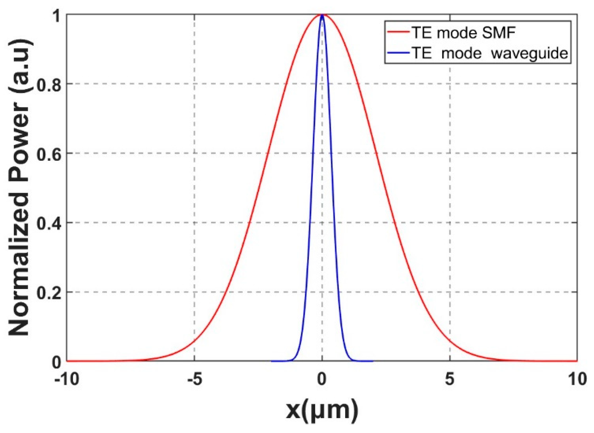
To comprehend the issue of the mismatch size between the Si3N4 waveguide mode and the standard SMF mode with dimensions of a core diameter of 8.2 μm and cladding diameter of 125 μm, an illustration of the mode solution profile at an operating wavelength of 1310 nm was simulated. Figure 2 displays the outcomes of the TE fundamental mode of the standard SMF depicted in red color, and the Si3N4 waveguide with dimensions of 500 × 760 nm is depicted in blue color. The width size was selected to ensure a single TE mode solution, and the Si3N4 thickness was optimized.
It is evident from the figure that a significant mode mismatch is obtained, resulting in a minimum energy loss of 80%. Thus, to improve the light coupling between the Si3N4 waveguide chip and the SMF, a GC is employed to increase the Si3N4 waveguide mode so that it is more suitable to the SMF mode, and as a result, the overlap area between the two modes is increased, which leads to more energy efficiency.
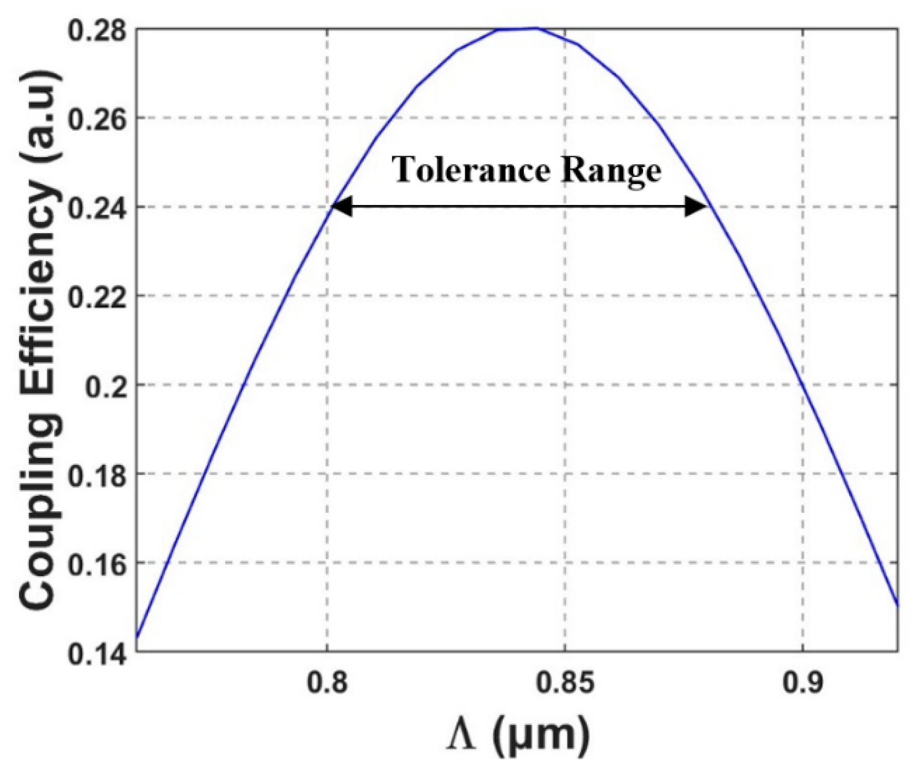
Figure 3 showcases the optimal grating period Λ in the GC waveguide, which is determined to be 0.84 μm. This carefully chosen value guarantees a robust configuration that can tolerate shifts of up to ±30 nm from the optimal value. With this grating period, light can propagate through the GC waveguide to the SMF in an exceptional manner, enabling efficient and reliable transmission. However, fabricating smaller grating periods demands the utilization of high-resolution lithography techniques, and achieving the desired resolution can pose significant challenges. This optimization is crucial for achieving high efficiency and ensuring good fabrication quality.
Figure 4 presents an essential analysis of the influence of etch depth on the coupling efficiency performance of the GC. Etch depth is a key fabrication parameter that governs the periodic corrugations etched into the GC structure. This parameter significantly impacts the interaction of light with the GC, thereby affecting the coupling efficiency and overall device performance. The graph showcases high coupling efficiency at an optimal value of 0.05 μm, yielding a coupling efficiency of 28%, with a tolerance range of ±0.05 μm from the optimal value. As a result, this range can be useful when handling fabrication errors that can happen at the fab faculty.
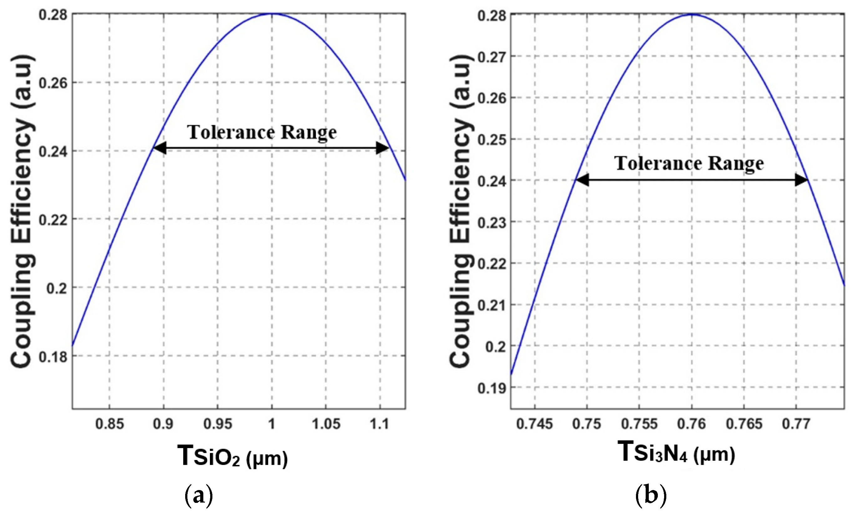
Figure 5a,b provide a visualization of the thickness of the SiO2 layer (TSiO2) and the Si3N4 thickness (TSi3N4) versus coupling efficiency to the SMF. In Figure 5a, it can be observed that a TSiO2 thickness of 1 µm demonstrates a high coupling efficiency of 28%, with a tolerance shift of ±25 nm. Figure 5b demonstrates the optimized value for TSi3N4, which is determined to be 0.76 µm, and the tolerance shift of ±30 nm ensures the allowable variation within this range. At this thickness, alongside the operation wavelength of 1310 nm, there is a reliable operation in the O-band spectrum. These findings provide valuable insights incorporated within the exact design criteria that are essential for attaining the intended GC performance, encompassing sturdy manufacturing processes.
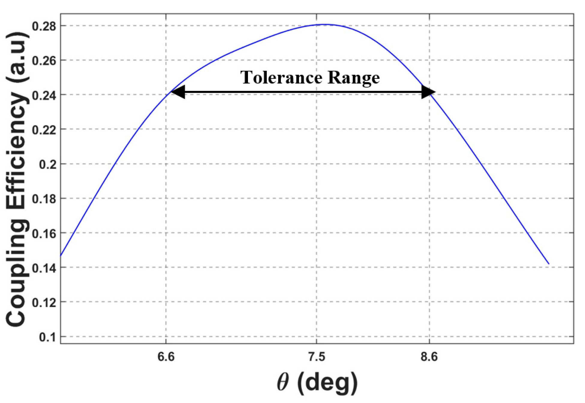
Figure 6 provides a detailed analysis of the coupling efficiency in relation to the angle of the SMF, which is located at a distance of 2.6 μm from the GC, specifically focusing on an operational wavelength of 1310 nm. The angle, denoted as θ, has been meticulously chosen to optimize the coupling efficiency between the GC and SMF. By utilizing the principles of Bragg conduction, alongside the FDTD simulations, the optimal angle has been found to be 7.5 degrees, as shown in Figure 6. Additionally, the figure also showcases a tolerance range spanning from 6.6 to 8.6 degrees. This range is particularly noteworthy as it demonstrates that even within this wide span of angles, the coupling efficiency is over 24%. This observation further emphasizes the robustness and effectiveness of the proposed design technology.
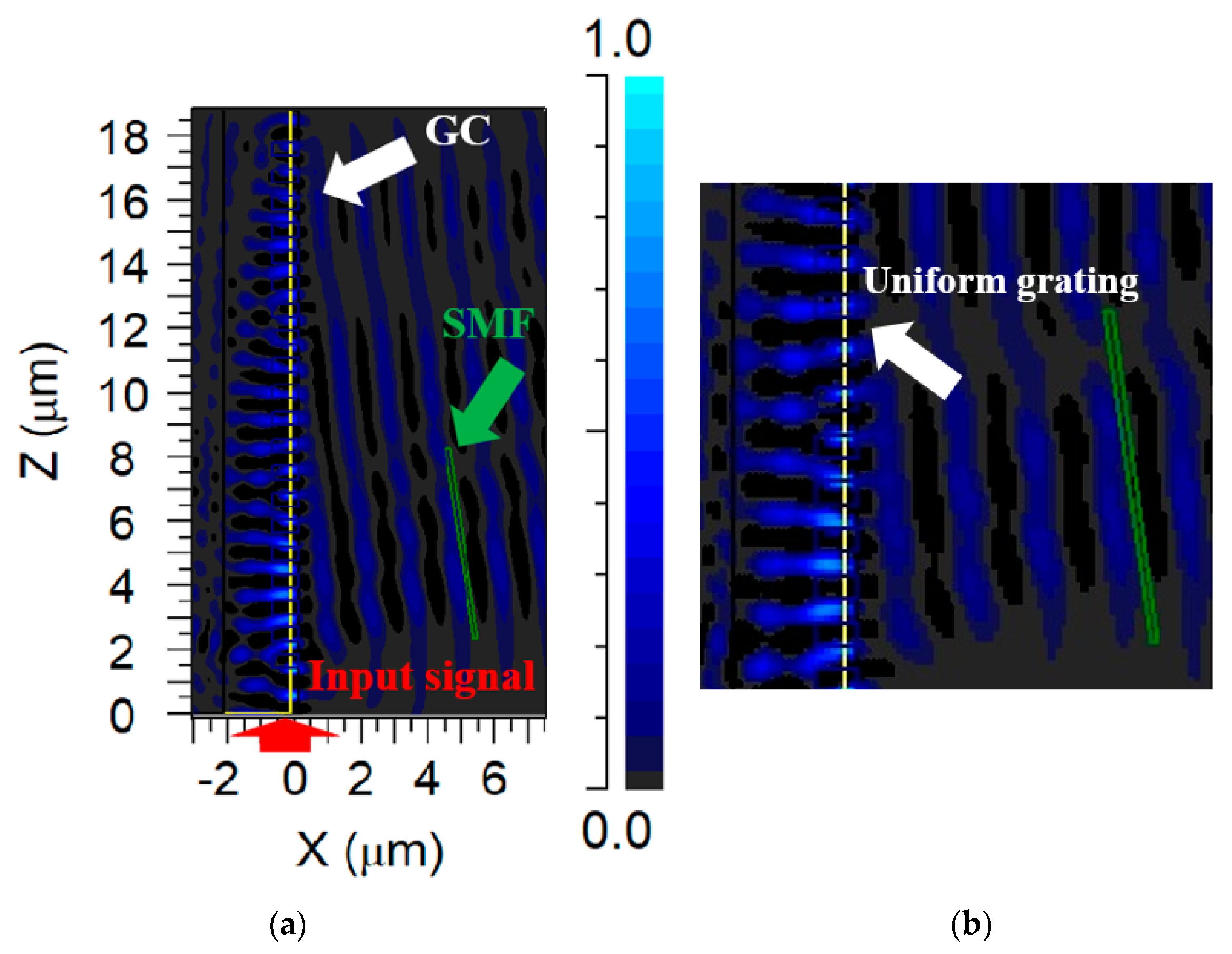
Figure 7 illustrates the scattered light within the GC directed towards the SMF at the x-z cross-section. The associated simulation depicts the intensity profile of the light being transmitted through the GC. A red arrow indicates the direction of the input signal, pointing towards the GC structure denoted by a white arrow, while a green arrow symbolizes the SMF. When examining the graph, it is evident that when the laser source transmits, the light scatters through the grating structure. Some of the light is absorbed by the SiO2 layer, while a portion propagates through the grating.
The phenomenon of light transmission through the grating can be observed in the middle of the graph where wave patterns emerge. These waves exhibit varying intensities, ranging from 0 (gray) to 1 (light blue), with the light blue color indicating higher intensity. The greater the intensity of these waves, the more light can be captured by the SMF. The process of light scattering through the GC is known as the Bragg effect, where there is a partial matching of phases between the incident wave and the scattered wave. As the waves propagate from the GC towards the SMF, their intensity increases, as indicated by a lighter shade of blue, and the coupling efficiency also improves. This implies that the integral overlap between the mode of the GC and the mode of the SMF increases. To better see the diffracted light coming from the GC into the SMF and the light scattering into the air, a zoom in on Figure 7a is conducted, as shown in Figure 7b.
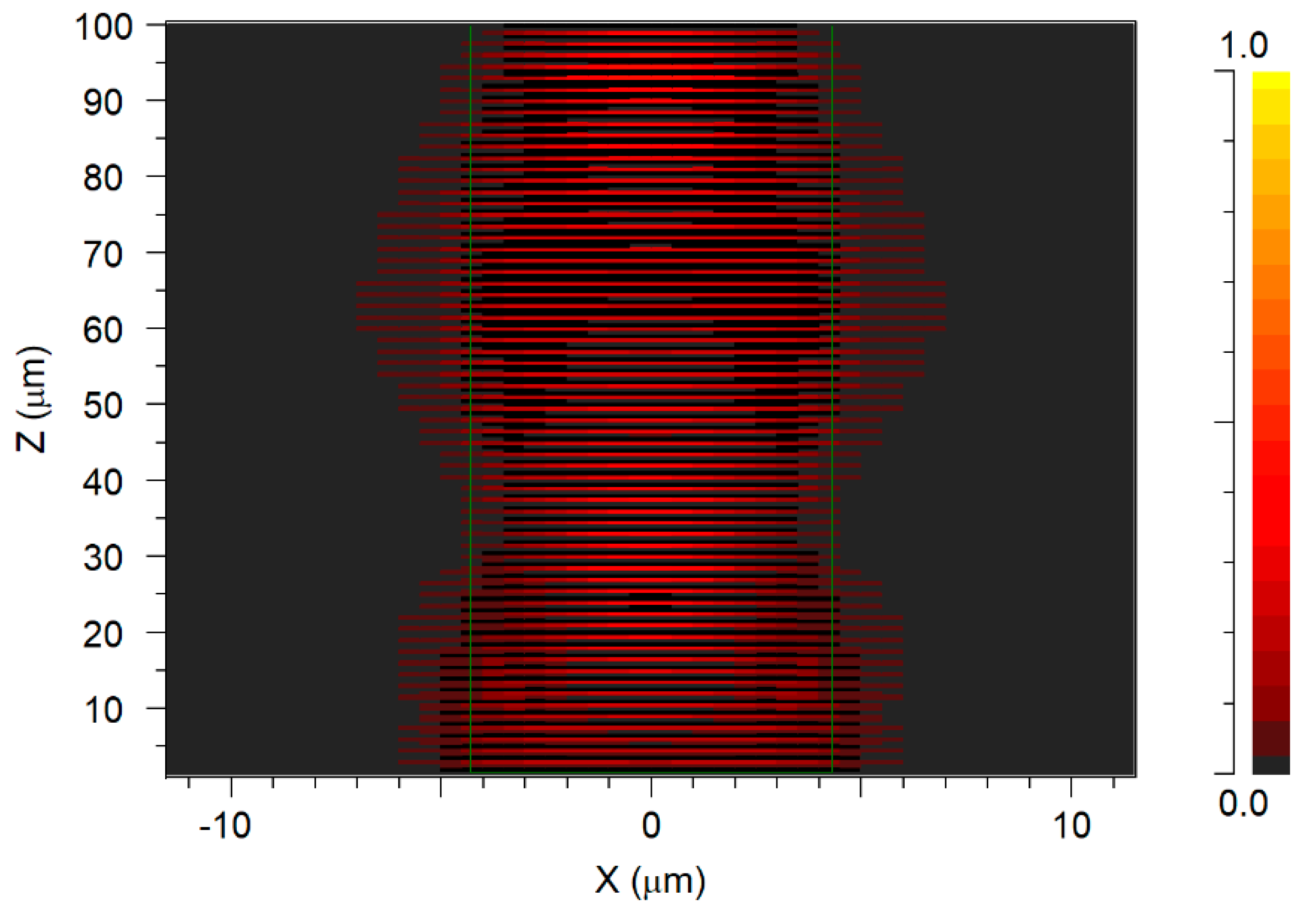
The output electric field from the FDTD monitor was extracted and used as a launch field to simulate and study the physical mechanism of the electric field distribution over the SMF, as shown in Figure 8. It can be seen that strong light confinement is achieved inside the SMF core, which ensures that all the light coupled from the GC can be utilized to test the signals at the output SMF.
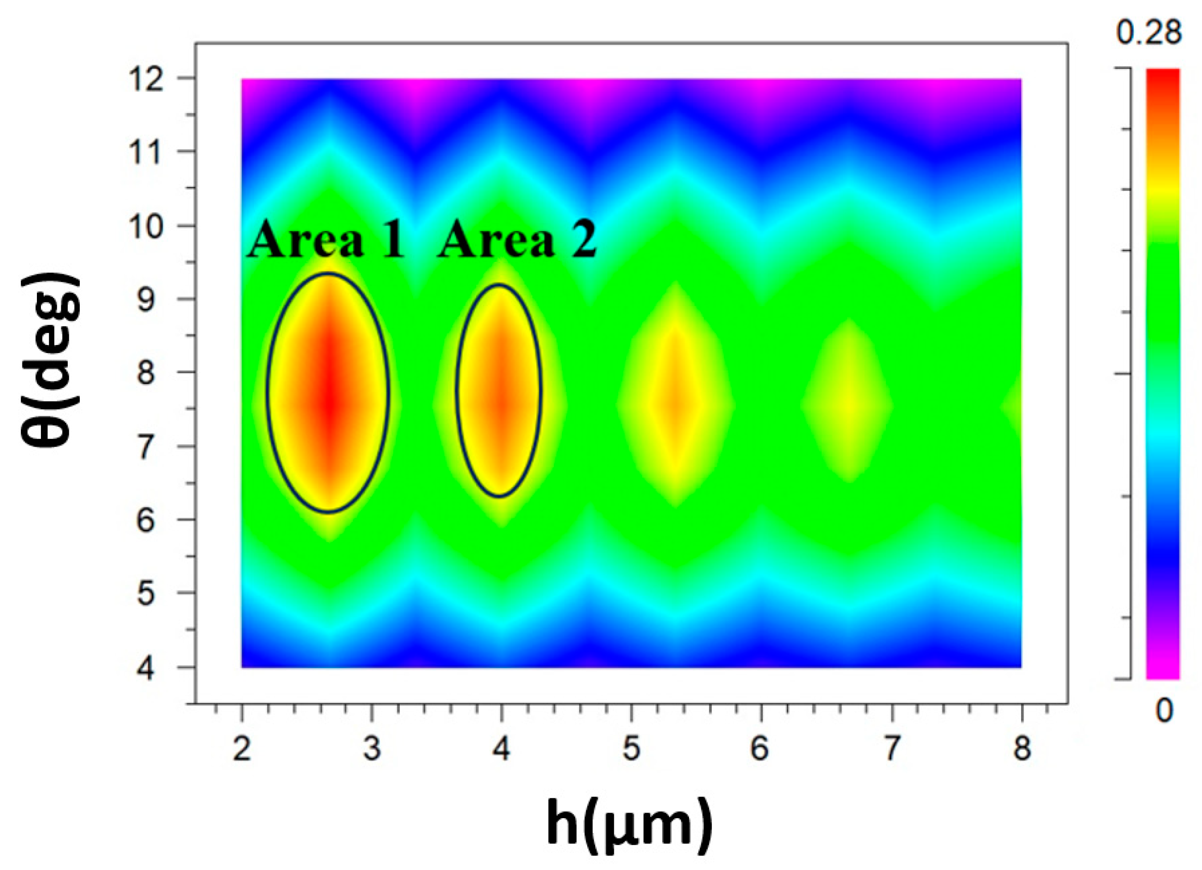
Figure 9 provides a comprehensive analysis of the coupling efficiency in relation to the SMF location from the GC. The graph illustrates two areas with strong coupling efficiency that can be utilized for the measurement of the chip signal. Additionally, the graph indicates a decrease in the coupling efficiency as h increases, which is clearly expected because of the absorption of the light in the free-space (air) zone. Thus, from a testing view, it will be better to use area 1 or area 2 to obtain good stability for dealing with mechanical errors, such as the shifting or vibrations of the SMF in the optical setup. Area 1 is located where h is between 2.2 and 3 μm, and θ is between 6.6 and 8.6 degrees. The maximum coupling efficiency is obtained at 2.6 μm, alongside 7.5 degrees. Area 2 is located where h is between 3.65 and 4.35 μm, θ is in the same range as the first area, and the maximum coupling efficiency is obtained at 4 μm, alongside 7.5 degrees. These results show a wide tolerance range of h with 400 nm and 350 for area 1 and area 2, respectively.
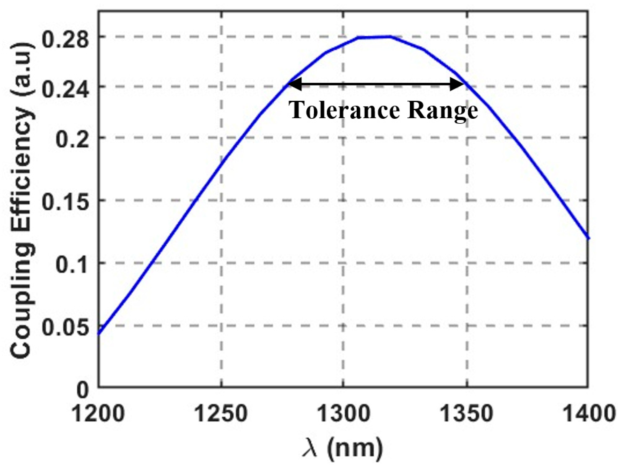
Figure 10 presents the coupling efficiency in relation to the wavelength in the O-band spectrum, specifically considering TE mode polarizations. The wavelength tolerance range spans from 1270 to 1360 nm, which is notably suitable for achieving a coupling efficiency of over 24%. Hence, our suggested GC device can readily manage the laser drift phenomenon, which can happen due to the heating process of the laser that can shift the wavelength around 0.08 nm/°C.
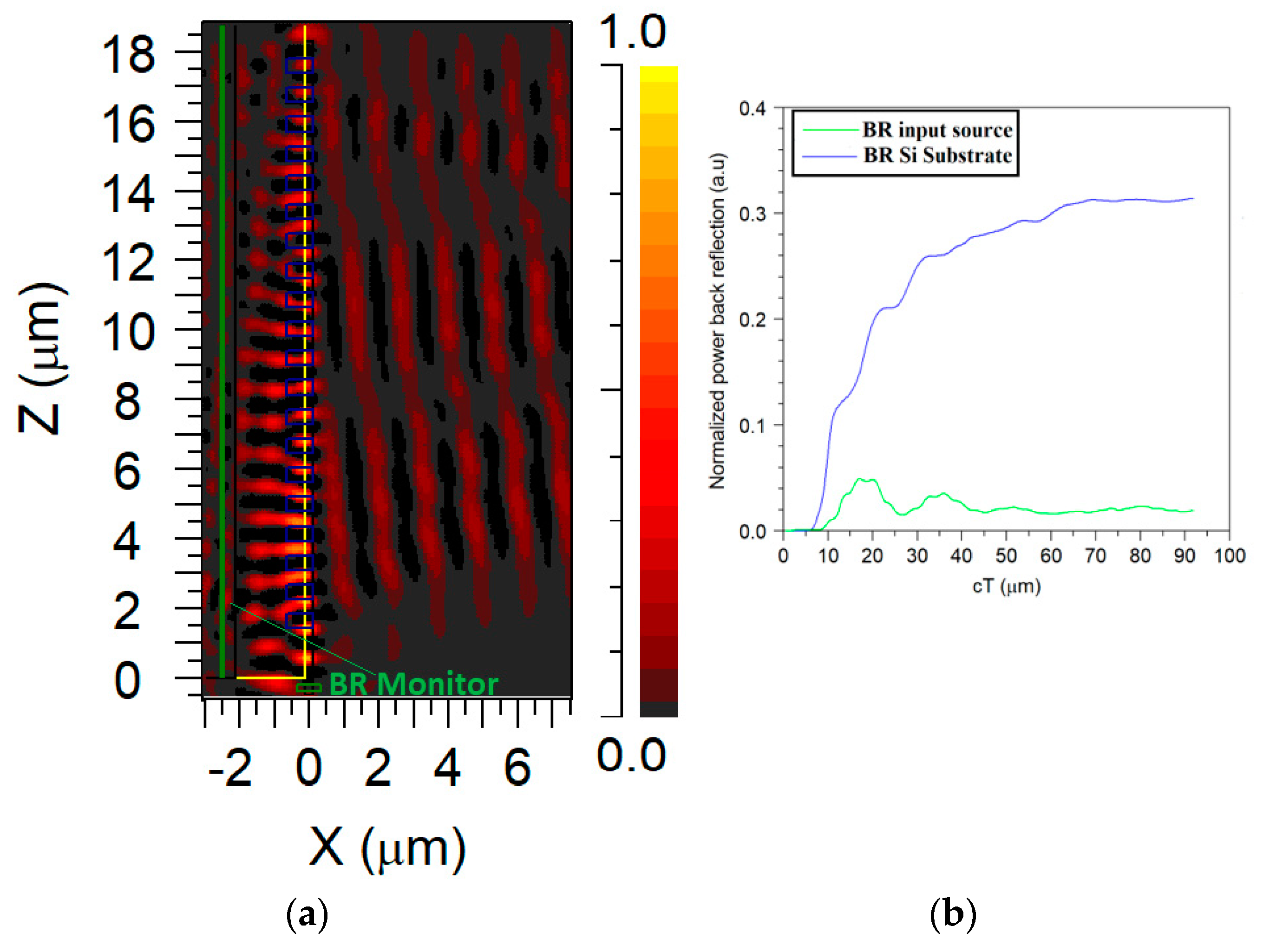
BR is another noteworthy facet of the GC. It can potentially pose substantial risks to the signal transmission because it can lead to undesired disturbances in the laser, which can reduce the signal integrity. To determine the BR power in our model, two monitors (green color in Figure 11a) were positioned. One was placed at the input of the GC waveguide to capture the entirety of the light that was reflecting from the GC region, as depicted in Figure 11a. Another one was located at the Si background substrate to collect all the diffraction light coming back from the rectangular teeth areas of the GC, as shown in Figure 11a. The FDTD BR results show that 31.5% of the input light comes back into the Si substrate layer, and a minor BR light of 0.015% is reflected into the input waveguide section, as shown in Figure 11b. Hence, integrating a mirror located at the bottom before the Si substrate area can dramatically improve the light coupling from 28% to around 50% and above. However, this solution is not recommended because of the high cost of fabrication, alongside a larger footprint size. The BR coming to the input signal can be handled easily by integrating a Si3N4 adiabatic waveguide taper, which can reduce it to 40 dB BR [43].
Table 1 presents an extensive comparison of Si3N4 on an insulator-based chip-to-fiber GC, involving essential factors such as Si3N4 GC technology, coupling efficiency, wavelength, complexity of fabrication, and fabrication costs. From this table, it can be seen that only a GC with a complex configuration alongside a high cost can obtain a higher coupling efficiency ranging from 38% to 56%. Our proposed device shows superior characteristics, such as a low cost with a simple configuration that is easy to fabricate, and can also be operated in the O-band spectrum. Thus, our GC is the most suitable GC to use for testing signals for PICs working in data center applications.
4. Conclusions
A new design of a GC based on Si3N4 structures for efficient light coupling in the O-band spectrum has been demonstrated. The proposed GC design, utilizing a uniformly grooved teeth rectangular configuration, offers improvements in terms of cost-effectiveness and ease of fabrication, compared to other GC models. Through numerical investigations using the FDTD method, the optimal key values of the GC have been found to fulfill the Bragg condition for increasing the Si3N4 waveguide TE mode. The optimal grating period (Λ) was determined to be 0.84 μm, ensuring robust performance even with slight deviations. The thicknesses of the SiO2 and Si3N4 layers were carefully chosen with a thickness of 1 μm for SiO2 and 0.76 μm for Si3N4, and the etch depth was set to be 0.36 μm with a tolerance range of ±0.05 μm. The coupling angle (θ) from the SMF was optimized at 7.5 degrees, and the distance between the SMF and GC was determined to be 2.6 μm, resulting in an excellent coupling efficiency of 28% between the GC and SMF at a wavelength of 1310 nm. Also, through simulation, the electric field distribution over the SMF has been studied and shows strong light confinement inside the SMF core, which helps us to maintain the optical energy at the SMF output for testing signals. In addition, two areas for testing measuring with high efficiency have been found, which can be useful to deal with mechanical errors in the optical setup. The proposed GC device can support the O-band spectrum with a high coupling efficiency of over 24%, and can easily handle the laser drift effect. The analysis of the proposed Si3N4-based GC with other designs and technologies highlighted its advantages in terms of cost-effectiveness, ease of fabrication, and performance. Based on the findings of the BR analysis, 31.5% of the input light is reflected into the Si substrate layer. This issue can be handled by putting a bottom mirror before the Si layer. However, this solution will increase the fabrication cost and complexity. Also, only a minimum of 0.015% BR power is coming back into the input waveguide, which can be easily handled by adding an adiabatic Si3N4 waveguide taper. By eliminating the need for a waveguide converter from Si3N4 to Si, our design minimizes power losses and BR, reducing the footprint size of the photonic chip and enabling better performances. Hence, the proposed Si3N4-based GC design offers a promising solution for efficient light coupling in the O-band spectrum. The optimized structural properties and design parameters contribute to high coupling efficiency, while the use of Si3N4 waveguides in PICs provides superior optical properties. Thus, the new design can be superior compared to the classical Si GC for testing Si3N4 photonic chips. From a system view, using our new design instead of the classical Si GC can improve the transceiver chip performances operating within the O-band spectrum.
Author Contributions
D.M. conceptualized the project. D.M. offered guidance and direction. E.O. devised the device’s design. E.O. conducted simulations with the assistance of D.M. E.O. authored the paper and response letter, and generated the figures. All authors have read and agreed to the published version of the manuscript.
Funding
This research received no external funding.
Institutional Review Board Statement
Not applicable.
Informed Consent Statement
Not applicable.
Data Availability Statement
The link provided below directs you to the article available on the HIT website within the library category: Article Link: [https://www.hit.ac.il/].
Conflicts of Interest
The authors declare no conflict of interest.
References
- Bowen, T.; Lee, J.; Ling, T.; Sun, J.; Zhang, H. Mode Size Converter Designs for Fabrication of Ultra-Low Loss Optical Interconnects. In Proceedings of the 2016 Pan Pacific Microelectronics Symposium (Pan Pacific), Big Island, HI, USA, 25–28 January 2016. [Google Scholar] [CrossRef]
- Zhang, Z.; Liu, T.; Zhang, K.; Li, M.; Liu, H.; Li, H.; Niu, P.; Gu, E. Bidirectional Grating Based Interleaved Angled MMI for High-Uniformity Wavelength Division (de)Multiplexing and Surface-Normal Fiber Packaging. Appl. Opt. 2021, 60, 5615. [Google Scholar] [CrossRef]
- Cheng, L.; Mao, S.; Li, Z.; Han, Y.; Fu, H.Y. Grating Couplers on Silicon Photonics: Design Principles, Emerging Trends and Practical Issues. Micromachines 2020, 11, 666. [Google Scholar] [CrossRef]
- Denisov, G.G.; Kalynova, G.I.; Sobolev, D.I. Method for Synthesis of Waveguide Mode Converters. Radiophys. Quantum Electron. 2004, 47, 615–620. [Google Scholar] [CrossRef]
- Wilmart, Q.; Dirani, H.E.; Tyler, N.A.; Fowler, D.; Malhouitre, S.; Garcia, S.; Casale, M.; Kerdiles, S.; Hassan, K.; Monat, C.; et al. A Versatile Silicon-Silicon Nitride Photonics Platform for Enhanced Functionalities and Applications. Appl. Sci. 2019, 9, 255. [Google Scholar] [CrossRef]
- Qing, F.-L.; Song, J.-F.; Luo, X.; Yu, M.; Lo, G.-Q.; Liu, Y. Mode-Size Converter with High Coupling Efficiency and Broad Bandwidth. Opt. Express 2011, 19, 21588. [Google Scholar] [CrossRef]
- Hosseini, A.; Covey, J.; Chen, R.T. Mode Order Converter Using Tapered Multi-Mode Interference Couplers. In Proceedings of the Integrated Photonics Research, Silicon and Nanophotonics 2010, Monterey, CA, USA, 25–28 July 2010. [Google Scholar] [CrossRef]
- Hu, J.-Y.; Lin, C.-P.; Hung, S.-Y.; Yang, H.; Chao, C.-K. Semi-Ellipsoid Microlens Simulation and Fabrication for Enhancing Optical Fiber Coupling Efficiency. Sens. Actuators A-Phys. 2008, 147, 93–98. [Google Scholar] [CrossRef]
- Jia, L.; Song, J.-F.; Liow, T.-Y.; Luo, X.; Tu, X.; Qing, F.-L.; Koh, S.-C.; Yu, M.; Lo, G.-Q. Low Loss/Large Tolerance Mode Converter between SiN Waveguide and Cleaved Single Mode Fiber. In Proceedings of the 2014 Optical Fiber Communications Conference and Exhibition (OFC), San Francisco, CA, USA, 9 March 2014. [Google Scholar] [CrossRef]
- Mu, J.; Guo, Q.-Y.; Deng, L.; Liang, H. A Novel Silicon Nitride Slot Waveguide. Proc. SPIE 2014, 9288, 296–302. [Google Scholar] [CrossRef]
- Bashirullah, R.; Mortazawi, A. A Slotted-Waveguide Power Amplifier for Spatial Power-Combining Applications. IEEE Trans. Microw. Theory Tech. 2000, 48, 1142–1147. [Google Scholar] [CrossRef]
- Bucio, T.D.; Khokhar, A.Z.; Mashanovich, G.Z.; Gardes, F.Y. N-Rich Silicon Nitride Angled MMI for Coarse Wavelength Division (de)Multiplexing in the O-Band. Opt. Lett. 2018, 43, 1251. [Google Scholar] [CrossRef]
- Ma, X.; Hu, H.; Liu, S.; Dong, R.; Qing, F.-L.; Chen, H. The Edge-Coupler of Fiber-to-Chip with Ultra-Low Coupling Loss Based on Double-Layer Silicon Waveguides. Front. Phys. 2022, 10, 1018624. [Google Scholar] [CrossRef]
- Li, Z.; Fan, Z.; Zhou, J.; Cong, Q.; Zeng, X.; Zhang, Y.; Jia, L. Process Development of Low-Loss LPCVD Silicon Nitride Waveguides on 8-Inch Wafer. Appl. Sci. 2023, 13, 3660. [Google Scholar] [CrossRef]
- Xiao, J.; Xu, L.; Sun, X. Design of an Ultracompact MMI Wavelength Demultiplexer in Slot Waveguide Structures. Opt. Express 2007, 15, 8300. [Google Scholar] [CrossRef] [PubMed]
- Nadeem, M.A.; Shaikh, H.; Rauf, M. Performance Measure on Efficient Wireless Data Transfer in Highly Conductive Medium. In Proceedings of the 2019 15th International Conference on Emerging Technologies (ICET), Peshawar, Pakistan, 2–3 December 2019. [Google Scholar] [CrossRef]
- Mak, J.C.C.; Wilmart, Q.; Olivier, S.; Menezo, S.; Poon, J.K.S. Silicon Nitride-on-Silicon Bi-Layer Grating Couplers Designed by a Global Optimization Method. Opt. Express 2018, 26, 13656. [Google Scholar] [CrossRef] [PubMed]
- Nambiar, S.; Muthuganesan, H.; Sharma, T.K.; Selvaraja, S.K. On-Chip Unidirectional Dual-Band Fiber-Chip Grating Coupler in Silicon Nitride. OSA Contin. 2018, 1, 864. [Google Scholar] [CrossRef]
- Zhang, Y.; He, Y.; Wang, H.; Sun, L.; Su, Y. Ultra-Broadband Mode Size Converter Using On-Chip Metamaterial-Based Luneburg Lens. ACS Photonics 2020, 8, 202–208. [Google Scholar] [CrossRef]
- Sharma, V.; Sinha, A.; Shenoy, M.R. Mode Size Converter Based on Periodically Segmented Liquid Crystal Core Waveguide. J. Light. Technol. 2022, 40, 4728–4734. [Google Scholar] [CrossRef]
- Shiraishi, K.; Matsumura, K.; Ohnuki, H.; Ohishi, I.; Suga, S. Integration-Oriented Lensed Fibers Having Long Working Distances and Wide Tolerances. In Proceedings of the Optical Fiber Communications, OFC, San Jose, CA, USA, 25 February–1 March 1996. [Google Scholar] [CrossRef]
- Remis, A.; Monge-Bartolome, L.; Paparella, M.; Gilbert, A.; Boissier, G.; Grande, M.; Blake, A.; O’Faolain, L.; Cerutti, L.; Rodriguez, J.B.; et al. Unlocking the Monolithic Integration Scenario: Optical Coupling between GaSb Diode Lasers Epitaxially Grown on Patterned Si Substrates and Passive SiN Waveguides. Light-Sci. Appl. 2023, 12, 150. [Google Scholar] [CrossRef]
- Shoji, T.; Tsuchizawa, T.; Watanabe, T.; Yamada, K.; Morita, H. Low Loss Mode Size Converter from 0.3 μm Square Si Wire Waveguides to Singlemode Fibres. Electron. Lett. 2002, 38, 1669. [Google Scholar] [CrossRef]
- Sisto, M.M.; Fisette, B.; Paultre, J.-E.; Paquet, A.; Desroches, Y. Novel Spot Size Converter for Coupling Standard Single Mode Fibers to SOI Waveguides. In Proceedings of the SPIE OPTO, San Francisco, CA, USA, 14 March 2016. [Google Scholar] [CrossRef]
- Yamasaki, S.; Uchida, Y.; Takahashi, M.; Hasegawa, J.; Yagi, T. Spot Size Converter with Cross-Vertical Taper for Low-Loss Coupling between ZrO2-SiO2 PLC and SMF. In Proceedings of the OFC 2014, San Francisco, CA, USA, 9–13 March 2014. [Google Scholar] [CrossRef]
- Taillaert, D.; Bogaerts, W.; Bienstman, P.; Krauss, T.F.; Van Daele, P.; Moerman, I.; Verstuyft, S.; De Mesel, K.; Baets, R. An Out-of-Plane Grating Coupler for Efficient Butt-Coupling between Compact Planar Waveguides and Single-Mode Fibers. IEEE J. Quantum Electron. 2002, 38, 949–955. [Google Scholar] [CrossRef]
- Taillaert, D.; Van Laere, F.; Ayre, M.; Bogaerts, W.; Van Thourhout, D.; Bienstman, P.; Baets, R. Grating Couplers for Coupling between Optical Fibers and Nanophotonic Waveguides. Jpn. J. Appl. Phys. 2006, 45, 6071–6077. [Google Scholar] [CrossRef]
- Masturzo, S.A.; Yarrison-Rice, J.M.; Jackson, H.E.; Boyd, J.T. Grating Couplers Fabricated by Electron-Beam Lithography for Coupling Free-Space Light into Nanophotonic Devices. IEEE Trans. Nanotechnol. 2007, 6, 622–626. [Google Scholar] [CrossRef]
- Ding, Y.; Ou, H.; Peucheret, C.; Yvind, K. Fully-Etched Apodized Fiber-to-Chip Grating Coupler on the SOI Platform with −0.78 DB Coupling Efficiency Using Photonic Crystals and Bonded Al Mirror. In Proceedings of the 2014 The European Conference on Optical Communication (ECOC), Cannes, France, 21–25 September 2014. [Google Scholar] [CrossRef]
- Vermeulen, D.; Selvaraja, S.K.; Verheyen, P.; Lepage, G.; Bogaerts, W.; Absil, P.; Van Thourhout, D.; Roelkens, G. High-Efficiency Fiber-to-Chip Grating Couplers Realized Using an Advanced CMOS-Compatible Silicon-On-Insulator Platform. Opt. Express 2010, 18, 18278. [Google Scholar] [CrossRef] [PubMed]
- Vivien, L.; Pascal, D.; Lardenois, S.; Marris-Morini, D.; Cassan, E.; Grillot, F.; Laval, S.; Fedeli, J.-M.; Melhaoui, L.E. Light Injection in SOI Microwaveguides Using High-Efficiency Grating Couplers. J. Light. Technol. 2006, 24, 3810–3815. [Google Scholar] [CrossRef]
- Zaken, B.B.B.; Zanzury, T.; Malka, D. An 8-Channel Wavelength MMI Demultiplexer in Slot Waveguide Structures. Materials 2016, 9, 881. [Google Scholar] [CrossRef]
- Xiao, Y.; Xu, Y.; Dong, Y.; Zhang, B.; Ni, Y. A 60 μm-Long Fiber-to-Chip Edge Coupler Assisted by Subwavelength Grating Structure with Ultralow Loss and Large Bandwidth. Photonics 2022, 9, 413. [Google Scholar] [CrossRef]
- Zhong, Q.; Veerasubramanian, V.; Wang, Y.; Shi, W.; Patel, D.; Ghosh, S.; Samani, A.; Chrostowski, L.; Bojko, R.; Plant, D.V. Focusing-Curved Subwavelength Grating Couplers for Ultra-Broadband Silicon Photonics Optical Interfaces. Opt. Express 2014, 22, 18224. [Google Scholar] [CrossRef] [PubMed]
- Zou, J.; Yu, Y.; Ye, M.; Liu, L.; Deng, S.; Xu, X.; Zhang, C. Short and Efficient Mode-Size Converter Designed by Segmented-Stepwise Method. Opt. Lett. 2014, 39, 6273. [Google Scholar] [CrossRef] [PubMed]
- Lee, B.-T.; Shin, S.Y. Mode-Order Converter in a Multimode Waveguide. Opt. Lett. 2003, 28, 1660. [Google Scholar] [CrossRef]
- Manolatou, C.; Haus, H.A. Compact Mode-Size Converters for Efficient Coupling between Fibers and Integrated Optical Waveguides. In Proceedings of the 2001 Digest of LEOS Summer Topical Meetings: Advanced Semiconductor Lasers and Applications/Ultraviolet and Blue Lasers and Their Applications/Ultralong Haul DWDM Transmission and Networking/WDM Compo, Copper Mountain, CO, USA, 30 July–1 August 2001. [Google Scholar] [CrossRef]
- Kumric, H.; Thumm, M.; Wilhelm, R. Optimization of Mode Converters for Generating the Fundamental TE01mode from TE06Gyrotron Output at 140 GHz. Int. J. Electron. 1988, 64, 77–94. [Google Scholar] [CrossRef]
- Xu, H.; Qin, Y.; Hu, G.; Tsang, H.K. Compact Integrated Mode-Size Converter Using a Broadband Ultralow-Loss Parabolic-Mirror Collimator. Opt. Lett. 2023, 48, 327. [Google Scholar] [CrossRef]
- Frishman, A.; Malka, D. An Optical 1 × 4 Power Splitter Based on Silicon–Nitride MMI Using Strip Waveguide Structures. Nanomaterials 2023, 13, 2077. [Google Scholar] [CrossRef] [PubMed]
- Brand, O.; Wolftson, B.; Malka, D. A Compact Polarization MMI Combiner Using Silicon Slot-Waveguide Structures. Micromachines 2023, 14, 1203. [Google Scholar] [CrossRef] [PubMed]
- Menahem, J.; Malka, D. A Two-Channel Silicon Nitride Multimode Interference Coupler with Low Back Reflection. Appl. Sci. 2022, 12, 11812. [Google Scholar] [CrossRef]
- Zou, J.; Yu, Y.; Ye, M.; Liu, L.; Deng, S.; Zhang, C. Ultra Efficient Silicon Nitride Grating Coupler with Bottom Grating Reflector. Opt. Express 2015, 23, 26305. [Google Scholar] [CrossRef]
- Doerr, C.R.; Chen, L.; Chen, Y.-K.; Buhl, L.L. Wide Bandwidth Silicon Nitride Grating Coupler. IEEE Photonics Technol. Lett. 2010, 22, 1461–1463. [Google Scholar] [CrossRef]
- Xu, C.; Khajavikhan, M.; LiKamWa, P. A Silicon Nitride Grating Coupler for Efficent Coupling Bewteen Waveguide and Fiber. In Proceedings of the 2017 IEEE Photonics Conference (IPC), Orlando, FL, USA, 1–5 October 2017. [Google Scholar] [CrossRef]
- Zhao, X.; Li, D.; Zeng, C.; Gao, G.; Huang, Z.; Huang, Q.; Wang, Y.; Xia, J. Compact Grating Coupler for 700-Nm Silicon Nitride Strip Waveguides. J. Light. Technol. 2016, 34, 1322–1327. [Google Scholar] [CrossRef]
- Zhang, H.; Li, C.; Tu, X.; Song, J.-F.; Zhou, H.; Luo, X.; Huang, Y.; Yu, M.; Lo, G.-Q. Efficient Silicon Nitride Grating Coupler with Distributed Bragg Reflectors. Opt. Express 2014, 22, 21800. [Google Scholar] [CrossRef] [PubMed]
Figure 1.
2D schematic diagram of the GC configuration and key parameters.

Figure 2.
Gaussian profile of the TE fundamental mode for SMF (red color) and Si3N4 waveguide (blue color).
Figure 2.
Gaussian profile of the TE fundamental mode for SMF (red color) and Si3N4 waveguide (blue color).

Figure 3.
Coupling efficiency as a function of grating period Λ.

Figure 4.
Coupling efficiency as a function of etch depth.

Figure 5.
Coupling efficiency as a function of thickness: (a) TSiO2, (b) TSi3N4.

Figure 6.
Coupling efficiency with respect to the angle from the SMF.

Figure 7.
Description of the intensity light propagation from the GC into the SMF: (a) x-z plane, (b) zoom into the GC area.
Figure 7.
Description of the intensity light propagation from the GC into the SMF: (a) x-z plane, (b) zoom into the GC area.

Figure 8.
Electric field distribution inside the SMF over the x-z plane.

Figure 9.
Optimizations of the SMF location from the GC.

Figure 10.
Variation of coupling efficiency with wavelength.

Figure 11.
BR calculations using FDTD method: (a) FDTD simulation setup, (b) normalized BR as a function of the optical path (cT, where c is the speed of light and T is time).
Figure 11.
BR calculations using FDTD method: (a) FDTD simulation setup, (b) normalized BR as a function of the optical path (cT, where c is the speed of light and T is time).


Table 1.
Comparative analysis of Si3N4 Insulator-Based Chip-to-Fiber GC.
| Si3N4 GC Technology | Coupling Efficiency (%) | Wavelength (μm) | Complexity of Fabrication (Yes/No) | Fabrication Cost (High/Low) |
|---|---|---|---|---|
| GC with bottom grating reflector [43] | 27 | 1.55 | yes | high |
| GC based on butt-coupled [44] | 38 | 1.54 | yes | high |
| GC between waveguide and fiber [45] | 22 | 1.56 | no | low |
| GC combined inverse taper using [46] | 42 | 1.56 | yes | high |
| GC with bottom reflectors [47] | 56 | 1.57 | yes | high |
| In this work | 28 | 1.31 | no | low |
Disclaimer/Publisher’s Note: The statements, opinions and data contained in all publications are solely those of the individual author(s) and contributor(s) and not of MDPI and/or the editor(s). MDPI and/or the editor(s) disclaim responsibility for any injury to people or property resulting from any ideas, methods, instructions or products referred to in the content. |
© 2023 by the authors. Licensee MDPI, Basel, Switzerland. This article is an open access article distributed under the terms and conditions of the Creative Commons Attribution (CC BY) license (https://creativecommons.org/licenses/by/4.0/).
Share and Cite
MDPI and ACS Style
Ohana, E.; Malka, D. O-Band Grating Couplers Using Silicon Nitride Structures. Appl. Sci. 2023, 13, 9951. https://doi.org/10.3390/app13179951
AMA Style
Ohana E, Malka D. O-Band Grating Couplers Using Silicon Nitride Structures. Applied Sciences. 2023; 13(17):9951. https://doi.org/10.3390/app13179951
Chicago/Turabian StyleOhana, Eli, and Dror Malka. 2023. "O-Band Grating Couplers Using Silicon Nitride Structures" Applied Sciences 13, no. 17: 9951. https://doi.org/10.3390/app13179951
Note that from the first issue of 2016, this journal uses article numbers instead of page numbers. See further details here.