Article

Design and Research of Intelligent Assembly and Welding Equipment for Three-Dimensional Circuit

1
College of Mechanical and Electrical Engineering, Nanjing University of Aeronautics and Astronautics, Nanjing 210016, China
2
No. 29 Research Institute of CETC, Chengdu 610036, China
3
School of Mechanical Engineering, Nanjing University of Science and Technology, Nanjing 210094, China
*
Author to whom correspondence should be addressed.
Appl. Sci. 2023, 13(16), 9359; https://doi.org/10.3390/app13169359
Submission received: 18 July 2023 / Revised: 14 August 2023 / Accepted: 15 August 2023 / Published: 17 August 2023
(This article belongs to the Special Issue Smart Manufacturing Systems in Industry 4.0)

Abstract

:
The processing of the three-dimensional circuit on the surface of conformal antennas is mainly performed via manual processing. At present, there is no automatic intelligent equipment for the processing of a similar small-sized circuit with variable curvature in China. Therefore, a high-precision, automated, full-process manufacturing method for three-dimensional circuits with flexible surfaces on conformal antennas of radar equipment has been proposed to improve processing quality and manufacturing efficiency. The processing relationship between solder paste spraying, resistor mounting, and laser welding in the flexible three-dimensional circuit manufacturing process was analyzed. The structure of the new conformal antenna three-dimensional circuit intelligent manufacturing equipment was determined, and simulation verification of the three-dimensional circuit processing was performed using Vericut. The optimal processing parameters were selected based on solid experiments. This method meets the electronic assembly requirements of radar equipment and fills the domestic gap.

1. Introduction

Military informatization is the inevitable trend of modern information war, and military electronics is an important link to improve the level of information technology of weapons and equipment. Among them, military radar is the primary visual sensor of combat system, which is crucial to target identification, target tracking, target location, missile guidance, etc., so it is regarded as the core system of military informatization [1,2,3]. With the development of microelectronics technology and large-scale integrated circuit technology, the fabrication of conformal antenna has become a research hotspot in the field of modern wireless communication antenna, and it has great application potential in the field of high-speed aircraft such as aircraft, missiles, and satellites [4,5,6,7] (As shown in Figure 1).
Conformal antennas can be divided into surface conformal antennas and structural conformal antennas. Surface conformal antennas are generally low-profile antennas that are laminated to the carrier surface to achieve a conformal effect [8]. Structural conformal antennas refer to antennas that are embedded inside the slot or slit on the surface of the carrier, embedded inside the carrier, and then installed in a flush manner to conform to the surface of the carrier to achieve a conformal effect [9]. Compared with the planar array antenna, the conformal array antenna will not disrupt the aerodynamic layout of the carrier, and the maneuverability of the aircraft will not be significantly affected. In addition, due to its curved surface characteristics, the conformal antenna makes full use of the surface area of the fuselage to obtain a larger aperture, achieving the goal of “small platform, large warning”.
The American MUSTRAP project [10] developed a structure integrated with a low cost. Through flight tests, it was found that the integrated antenna improved the low-frequency signal-to-noise ratio by 15~25 dB compared with the traditional blade antenna. Sang et al. [11] developed a CLSAAS design for a Ku-band satellite communication array antenna, which consisted of 64 array antenna patches. The antenna structure design was verified through simulation analysis and experiments, and the electrical performance of the antenna array was improved by optimizing the arrangement and spacing of radiation units. In China, Han Lei et al. [12], from the Air Force Engineering University, proposed the use of hybrid 3D printing technology to process airborne ultra-wideband conformal antennas, and they verified that the conformal antennas processed via this method met the performance requirements through standing wave testing and directional pattern testing. Peng Junjie et al. [13] at Peking University designed an array antenna based on polyimide films which can operate in the P-band with a wide scanning angle. The finite dipole array of the conformal antenna achieved a fractional bandwidth of 16.7% and a wide scanning angle range of ±60° in the E-plane.
The working ability of conformal antennas benefits the “specialness” of a curved conformal surface, but its manufacturing difficulty is also affected by the characteristics of the surface. Conformal antenna surface circuit manufacturing involves integrated processes on arbitrary free-form surfaces; under the commonly used planar circuit manufacturing process, it is difficult to meet the processing needs of the surface circuits, and there is usually a need to use the planar manufacturing circuit technology to create planar flexible circuits through the transfer printing technology to attach to the surface to achieve conformality [14] (As shown in Figure 2). Currently, the challenges of direct processing of antenna circuits on curved surfaces can be addressed through various manufacturing techniques such as printing manufacturing technology [15,16,17], inkjet print manufacturing technology [18,19,20], holographic lithography technology [21], microfluidic technology [22], and screen printing technology [23]. However, these manufacturing techniques have high material requirements, complex fabrication processes, and low efficiency. In addition, for large curvature shape structures, when the planar flexible circuit is attached to the surface, it is particularly difficult to process the surface circuit twice, such as mounting a resistor and welding. The above work needs to be performed with the help of an SMT machine. Currently, the international SMT machine market is mainly represented by Japan’s Panasonic, YAMAHA, FUJI (FUJI), and American Universal and Siemens of Germany, among which the mounter equipment produced by Japanese enterprises occupies most of the SMT market. Taking the equipment produced by Panasonic as an example, Panasonic’s NPM-D3A model features a dual-drive linear motor and a field-expandable multi-function identification camera that uses 3D recognition technology for accurate positioning and high positioning efficiency. In high-speed production mode, the mounting efficiency can reach 38,000 CPH (0.095 s/chip), and the mounting accuracy is controlled at ±30 μm/chip. The CPM-F series SMT machine developed by Shenzhen Luyuan Intelligent Equipment Company adopts industrial linear camera scanning recognition and magnetic suspension motion module, and the speed can reach 28,000 CPH. The mounting accuracy is ±0.05 mm, which has reached the high level of China’s domestic SMT machine. The SMT equipment of these mainstream manufacturers can realize the high precision and fast mounting of planar circuits. There is no mature equipment for the intelligent assembly and welding of a conformal antenna surface three-dimensional circuit, and the assembly and welding of resistors can only rely on manual operation [24]. This production method has problems such as high production difficulty, poor batch consistency, and low efficiency. Manual assembly and welding cannot meet the requirements for quality reliability and stability. With the continuous development and iteration of electronic warfare equipment such as fighter jets, missiles, and satellites, the market demand for conformal antennas is huge, and the assembly and welding technology of surface resistors has become a bottleneck restricting the development of conformal antennas. Therefore, developing a set of intelligent assembly and welding equipment for three-dimensional circuits is crucial for the development of electronic warfare equipment.

2. Planning and Design of Intelligent Assembly and Welding Equipment for Three-Dimensional Integrated Circuits

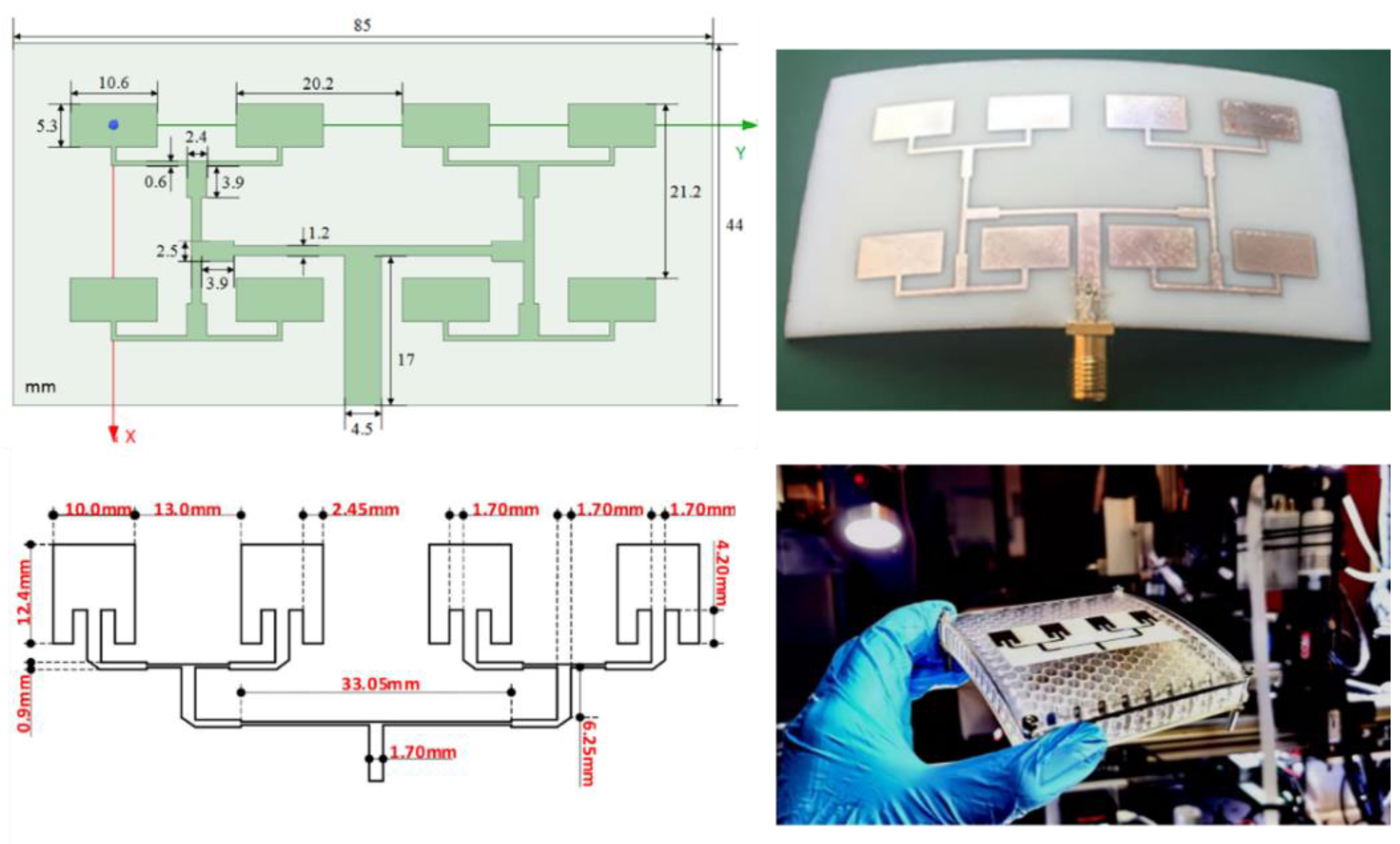
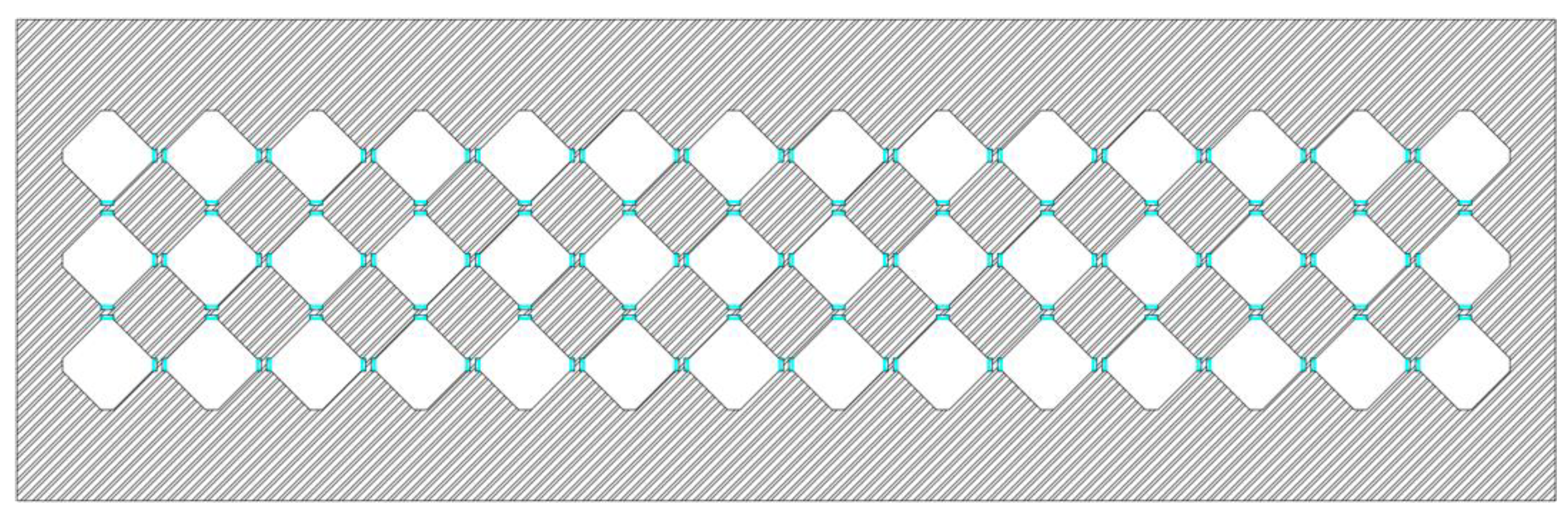
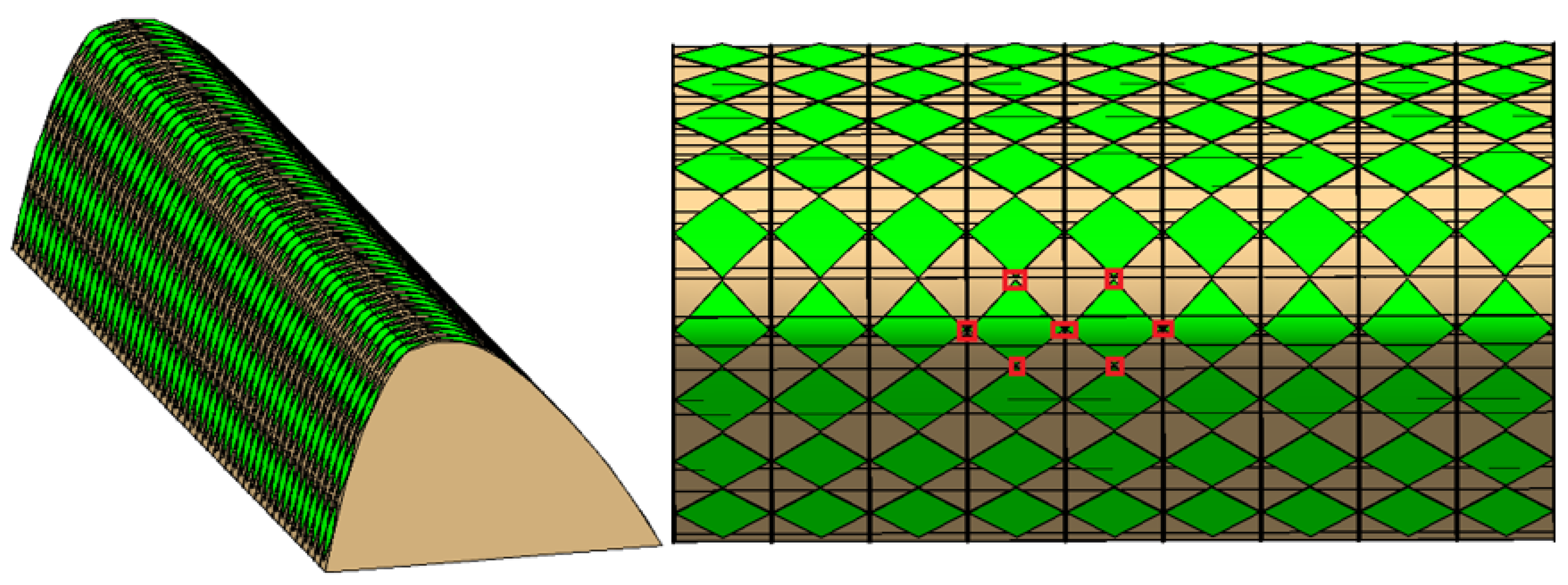
2.1. Introduction to Three-Dimensional Integrated Circuits on Conformal Antenna Surfaces

The prerequisite for the high-precision array antenna radar to achieve the expected functions is to ensure the high-quality processing of the three-dimensional circuit on the common antenna surface. The planar unfolding and processing point positions of the flexible three-dimensional circuit are shown in Figure 3. The processing point positions are connected to the radiation surface, with an area no greater than 0.75 mm2. A resistor with a mounting area of approximately 0.125 mm2 is mounted on the processing point to connect the circuit and achieve the flexible circuit function.
Due to the influence of the conformal antenna’s surface characteristics, when a three-dimensional circuit is attached to the conformal antenna surface, the outer shape becomes an irregular and variable curvature shape, as shown in Figure 4. The red circle shows the position distribution of the processing points. The processing steps involving solder paste spraying, resistor mounting, and laser welding are required to complete the assembly and welding of the circuit.

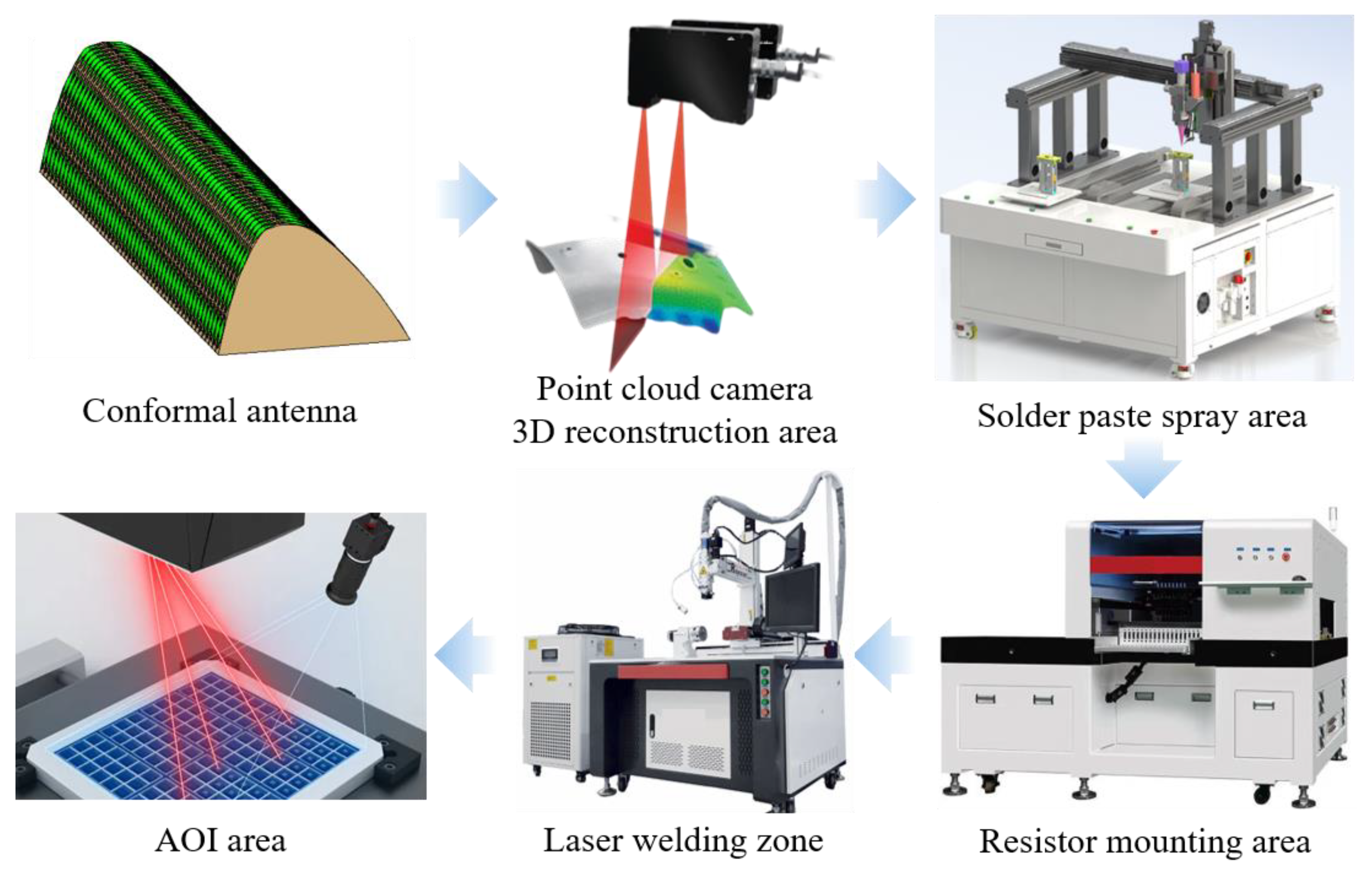
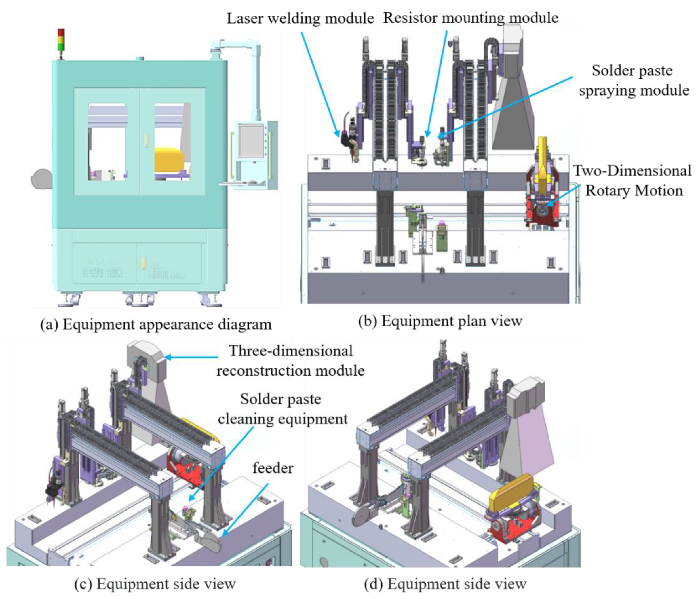
2.2. Overall Equipment Function Planning

In order to overcome the difficulties of the processing three-dimensional circuit processing on the surface of a conformal antenna, such as high personnel dependence and poor batch consistency, the equipment functions are divided into three functional modules: solder paste spraying, resistor mounting, and laser welding. To achieve high-precision processing at the end, a multi-object recognition algorithm that integrates gray-scale features and image pyramid technology is introduced to achieve high-precision visual guidance and position compensation for all functional modules. Based on fully automatic high-precision spraying technology and using process database parameters, a solder paste spraying module is designed that can adaptively spray solder paste for processing points. To achieve high-quality welding of flexible circuits, a resistor mounting module is designed based on force/position coupled smooth motion control technology, which achieves high-quality mounting of resistor chips through smooth control. Based on the relational evaluation model of laser welding process parameters such as laser welding power, spot size, and heating curve, a laser welding module is designed to achieve high-quality welding of small-sized processing points. Considering the geometric deviation between actual processed workpieces and theoretical processed workpieces, a visual detection module is introduced. The tasks of the visual detection module include the following: (1) Before the start of the machining task, the three-dimensional reconstruction of the actual workpiece is carried out to obtain the actual machining point coordinates. (2) Take pictures to identify the processing points after welding to achieve post-welding AOI detection.
The four main functional modules introduced above constitute a set of three-dimensional circuit intelligent assembly and welding equipment, and the overall process solution is shown in Figure 5.

3. Overall Equipment Scheme Design

The overall structural design of the intelligent assembly and welding equipment for three-dimensional circuits is shown in Figure 6. The equipment includes a three-dimensional reconstruction architecture module, a solder paste spraying module, a resistor mounting module, a laser welding module, a two-dimensional rotary motion module, as well as loading and unloading devices called feeders, and solder paste cleaning equipment.

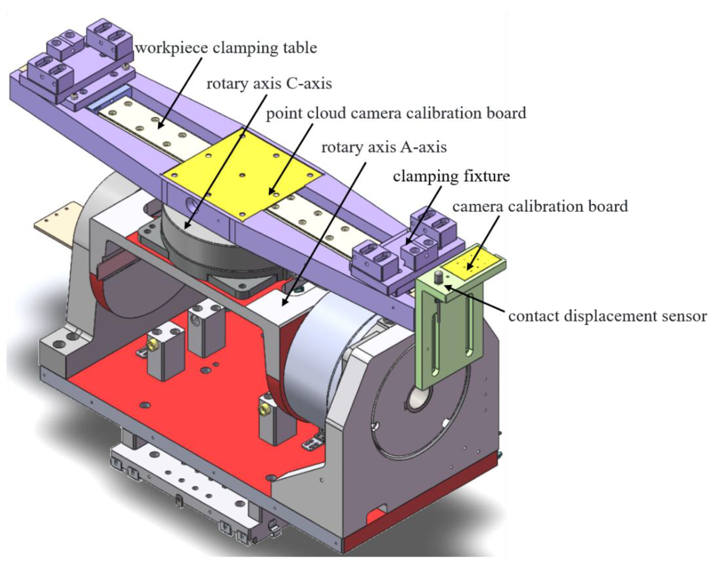
3.1. Design of Two-Dimensional Rotary Motion Module

Due to the special geometric shape of three-dimensional circuits, in order to ensure that the processing point on the curved surface is perpendicular to the mechanical end effector during processing, a two-dimensional rotary motion module is designed. The overall structure of the module is shown in Figure 7, which consists of a clamping fixture, a high-precision AC dual-axis rotation mechanism, a point cloud camera calibration board, a CCD camera calibration, and a contact displacement sensor. Through the rotation of the A-axis and the C-axis, the processing point on the surface can be rotated to the ideal position during machining. At the same time, since there are many processing steps, the two-dimensional rotary motion module is also responsible for driving the workpiece to various stations for processing.

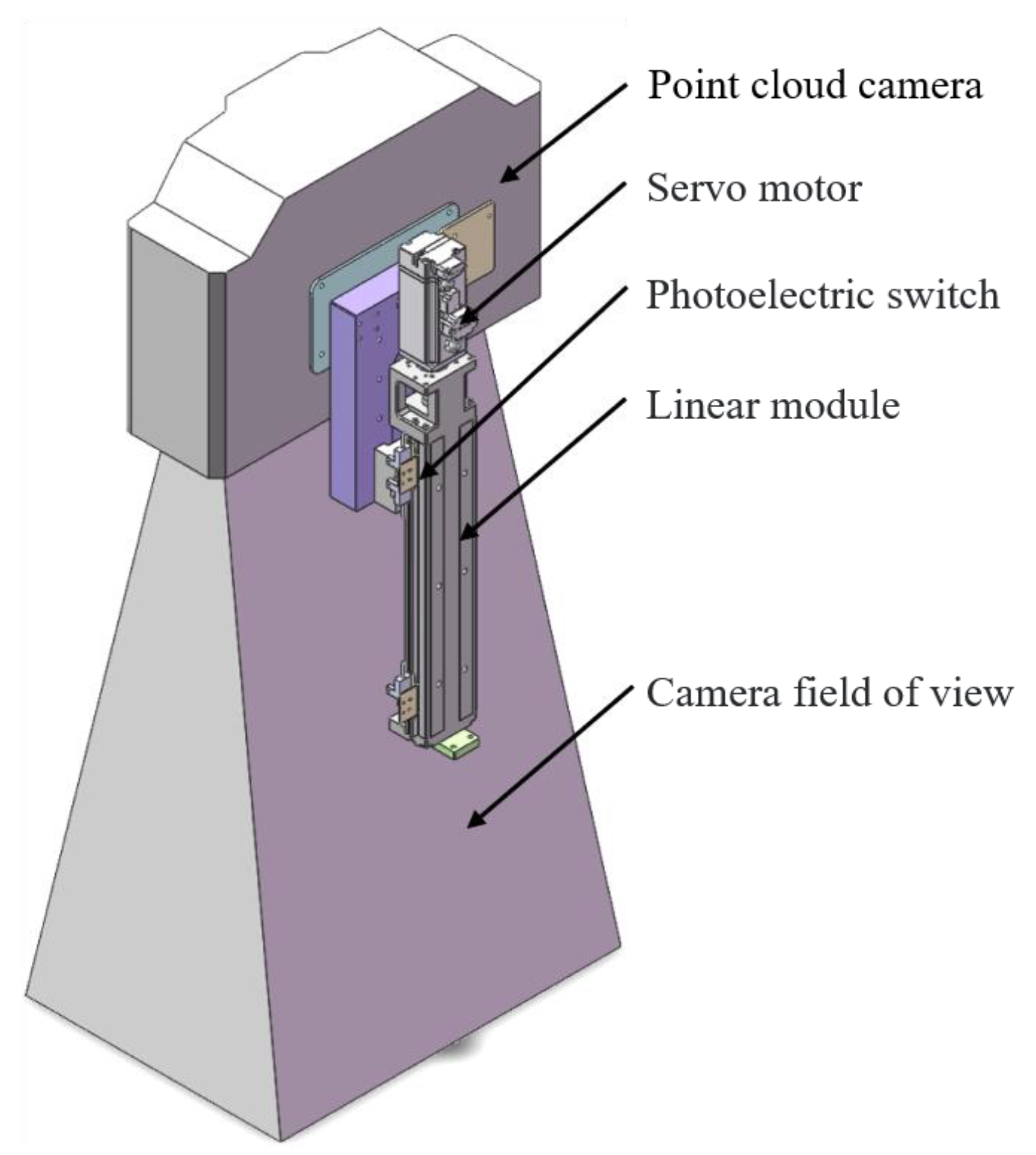
3.2. Design of Three-Dimensional Reconstruction Architecture Module

Most traditional spraying, patching, and welding equipment is designed for two-dimensional circuit designs. The manufacturing process of plant PCB is mature, with high processing quality and low processing errors. As a result, laser scanning or point cloud cameras are generally not required to compensate for the errors between theoretical circuits and actual fabricated circuits. The three-dimensional circuit proposed in this paper does not have the high precision of PCB. To improve the processing accuracy of three-dimensional circuit manufacturing, a three-dimensional reconstruction architecture module is designed based on the structured light three-dimensional surface rapid reconstruction technology. The module can identify the error between the actual model and the theoretical model, and it can obtain the normal vector of the machining point through the fitting surface technology, which provides the data basis for the subsequent processing. The mechanical structure of the module consists of a servo motor, linear guide, point cloud camera, and photoelectric switch. The overall structure is shown in Figure 8.
During the manufacturing process, the workpiece is first move to the three-dimensional reconstruction architecture module and then turn to the three-dimensional reconstruction position through the two-dimensional rotary motion module, while the point cloud camera is moved to a suitable field of view range via linear guide. Through three-dimensional point cloud reconstruction, the current workpiece’s placement posture and actual model data are obtained, and subsequent processing is adjusted and planned based on the above data.

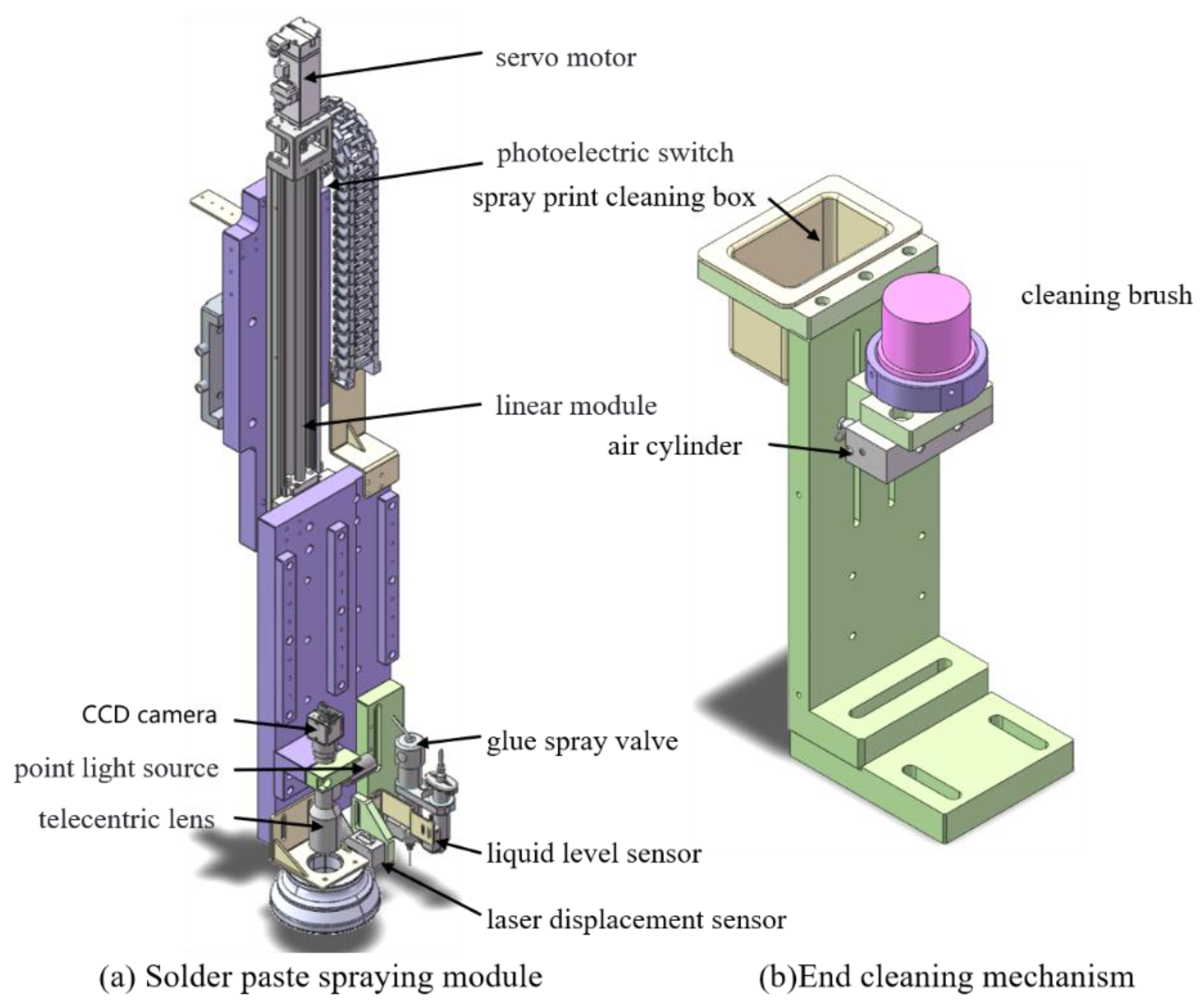
3.3. Design of Solder Paste Spraying Module

The main function of the solder paste spraying module is to spray solder paste on the processing points before mounting resistors. The module consists of a CCD camera, linear module, glue spray valve, liquid level sensor, and laser displacement sensor, and it is equipped with a spray print cleaning box. The mechanical structure is shown in Figure 9. Considering the high quality and precision requirements of small-sized circuit processing, the solder paste spraying method is adopted, and the CCD camera is designed to achieve positioning compensation during the processing. Solder paste spraying is the first step in the entire equipment processing, which has a huge impact on the quality of resistor mounting, laser welding, and even the entire circuit processing effect. Therefore, the module is designed with a glue valve and a liquid level sensor to execute appropriate solder paste spraying volume based on process database data to achieve precise solder paste spraying.

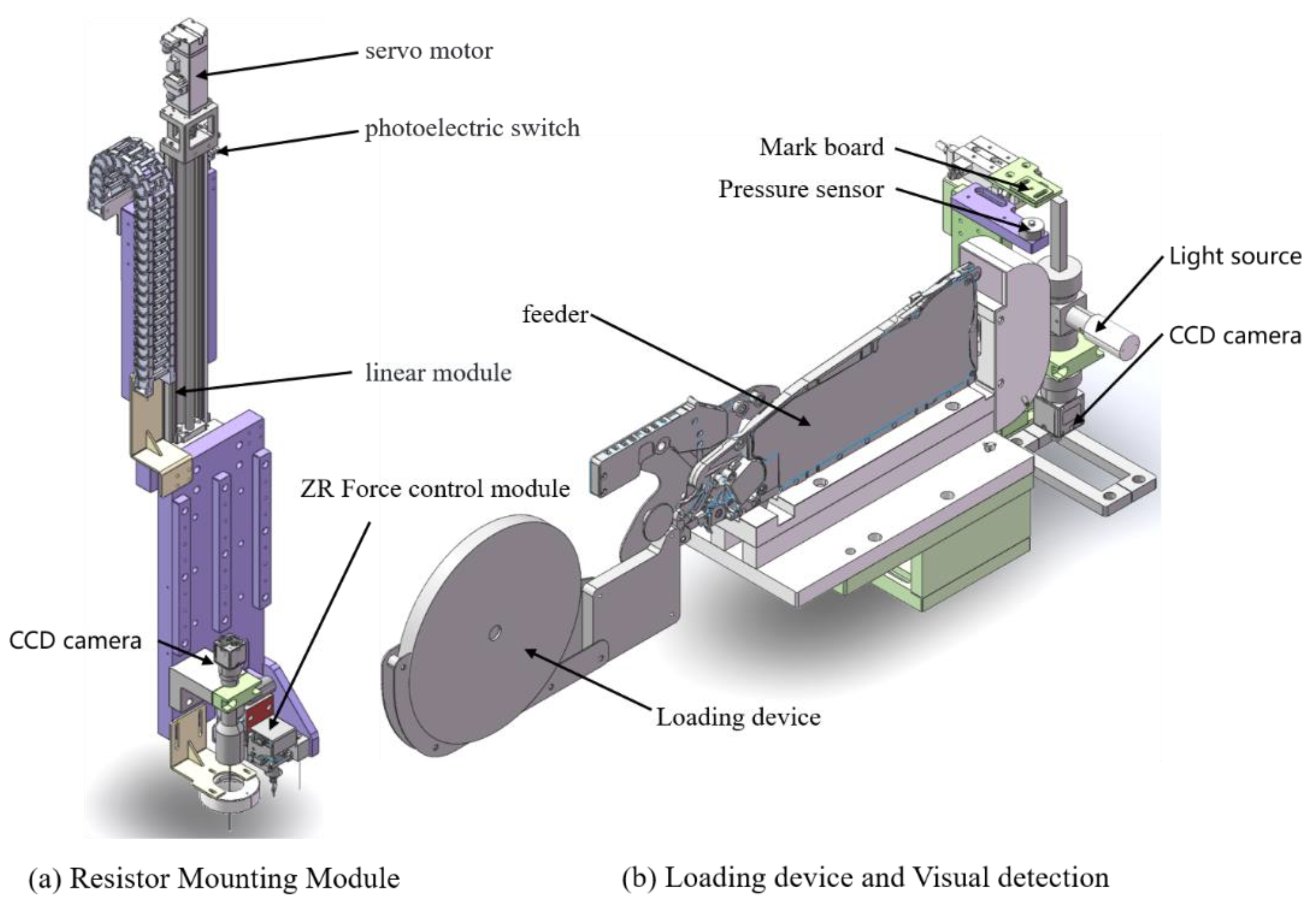
3.4. Design of Resistor Mounting Module

To achieve precise mounting of resistors, we designed a ZR force control module. By using contact detection and pressure detection, we established position, speed, and pressure change curves, analyzed the factors affecting the C/T time of the pressure assembly, and integrated a force/position coupling smooth motion control technology based on fuzzy PID control to control the steady-state pressure accuracy and prevent pressure over-shoot [26,27,28]. The mechanical structure of the entire module is shown in Figure 10, which consists of a ZR force control module, linear module, a pressure sensor, a CCD camera, a loading device, a feeder, and a calibration mechanism [29,30,31].
After completing the solder paste spraying, the two-dimensional rotary motion module drives the workpiece to resistor mounting position. The ZR force control module picks up the resistor from the feeder system and executes the position coordinate information of the solder paste spraying module to mount the resistor on the processed point after solder paste spraying.

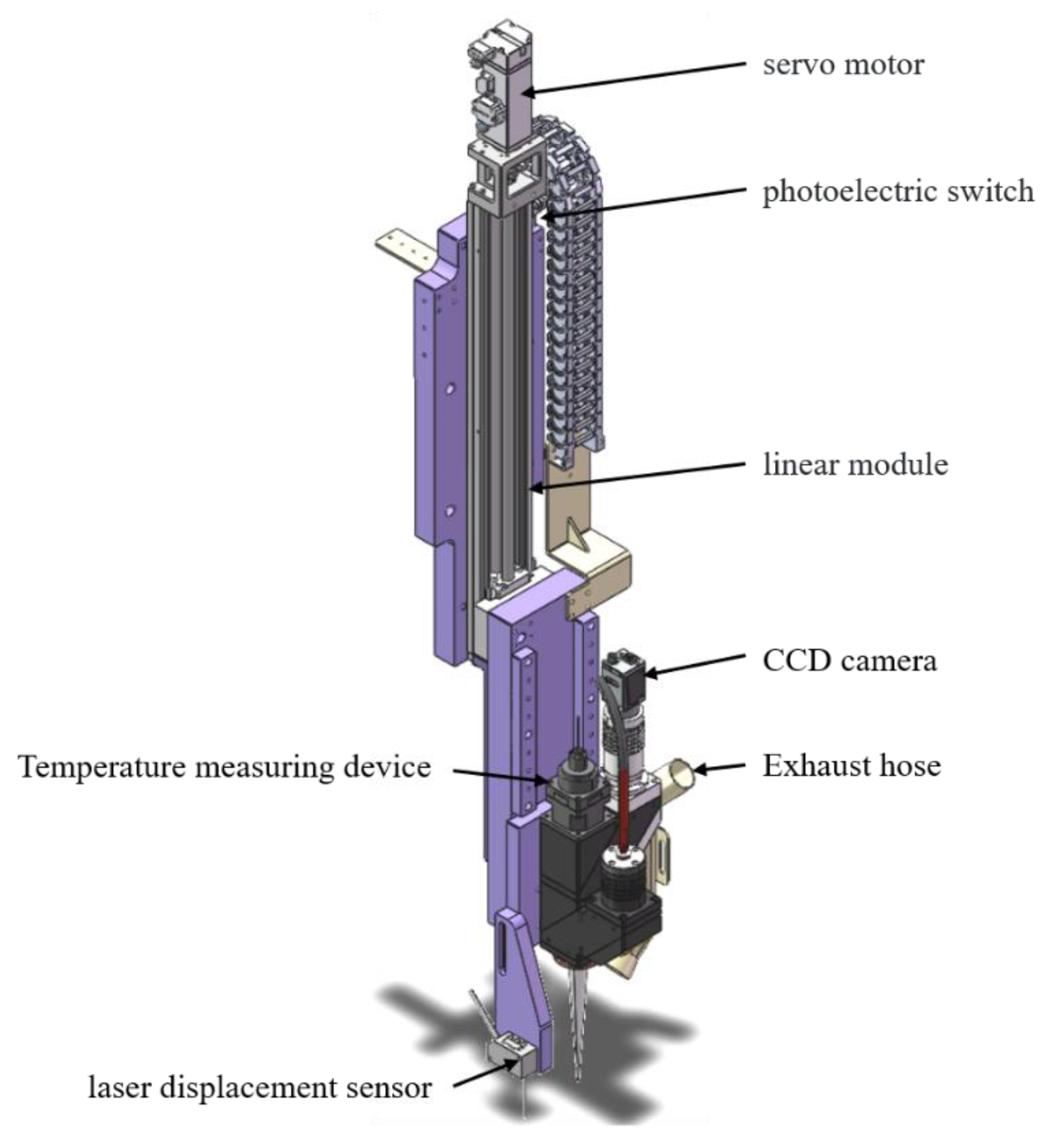
3.5. Design of Laser Welding Module

The traditional soldering method cannot realize the precision welding of small devices, and contact welding has the hidden danger of damaging the wire and transmission performance, which can also easily interfere with and affect the welding process. Therefore, this article designed a laser welding module that uses non-contact welding with a precision of micro-sized light spots, which is far superior to traditional methods. This processing method is clean and simple. The overall mechanical structure of the module is shown in Figure 11, which consists of a servo motor, a photoelectric switch, a temperature-measuring device, an exhaust pipe, a laser displacement sensor, a CCD camera, and a linear module.
After completing the resistor mounting, the two-dimensional rotary motion module drives the workpiece to the laser welding module, where it executes the position coordinate information of the resistor mounting module to perform laser welding on the processed points after mounting. During the welding process, this article adopts a temperature-controlled dynamic balance system to ensure the stability of the welding points. After completing the solder paste spraying, resistor mounting, and laser welding, the CCD camera of the laser welding module takes post-welding photos of the processed points and selects points with poor welding or insufficient welding for reprocessing [32].
Since the amount of solder paste spraying and laser welding parameters have a significant impact on the processing quality, it is necessary to select appropriate solder paste spraying amounts and laser welding parameters. The optimal parameters are shown in Table 1, and the processing experimental results are shown in Figure 12, which demonstrates good processing performance.

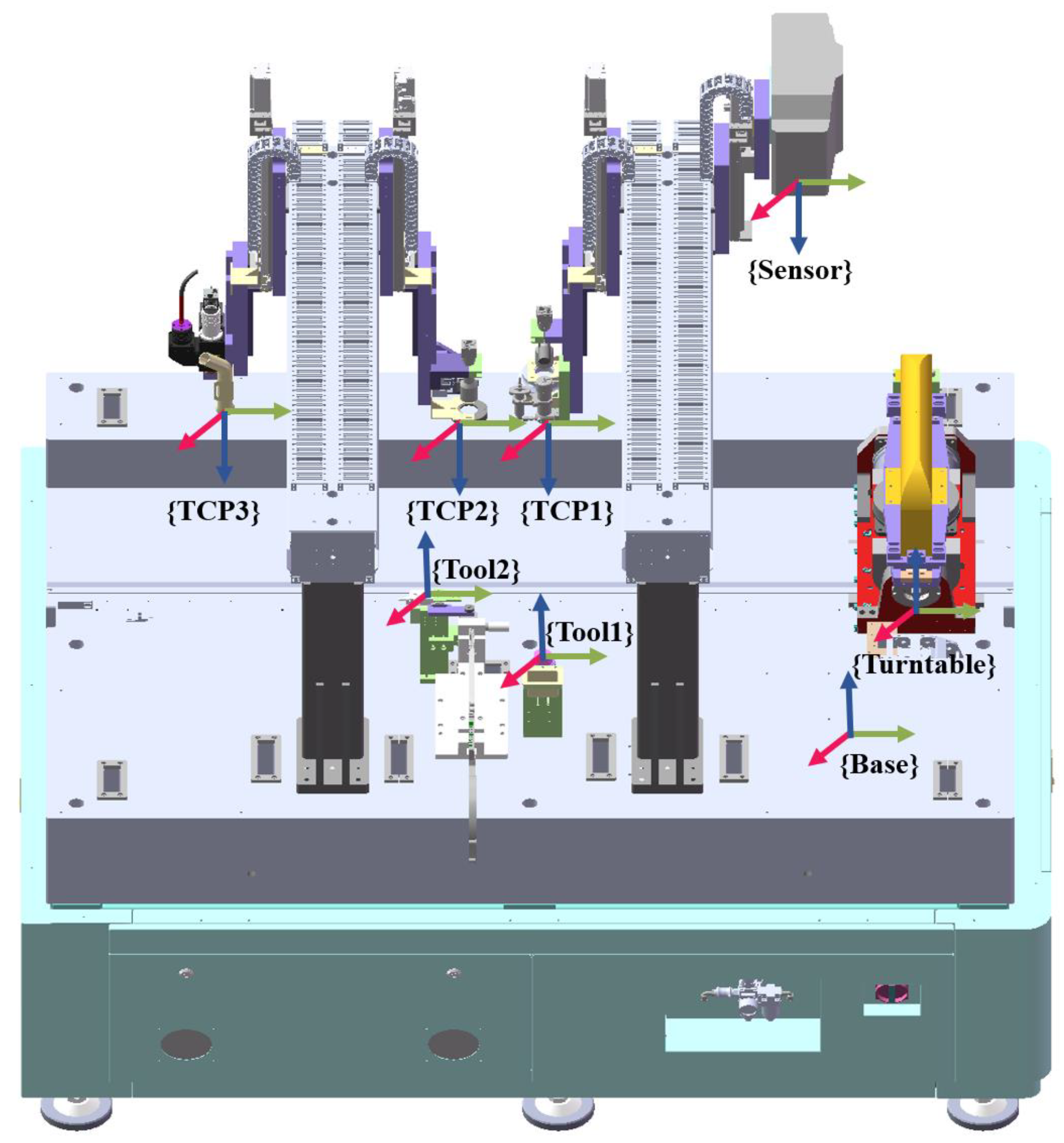
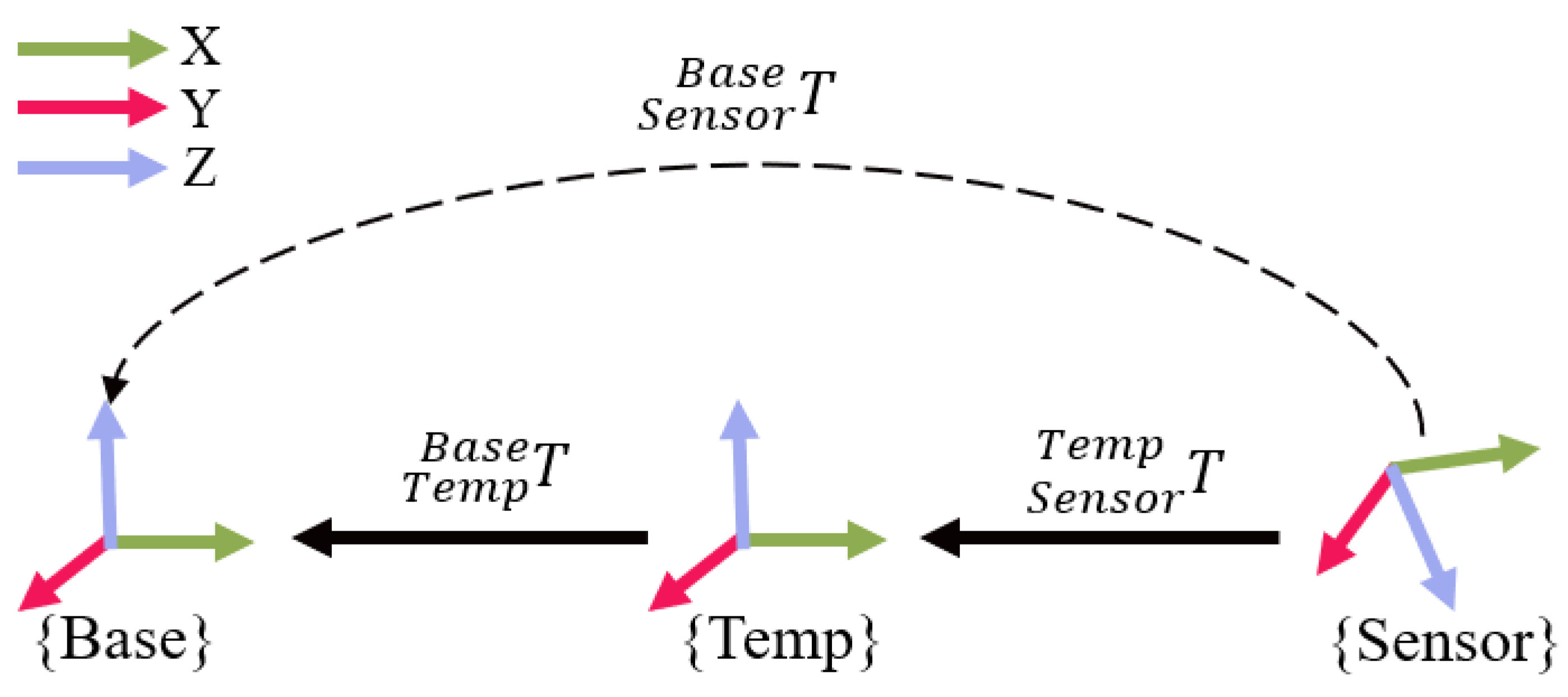
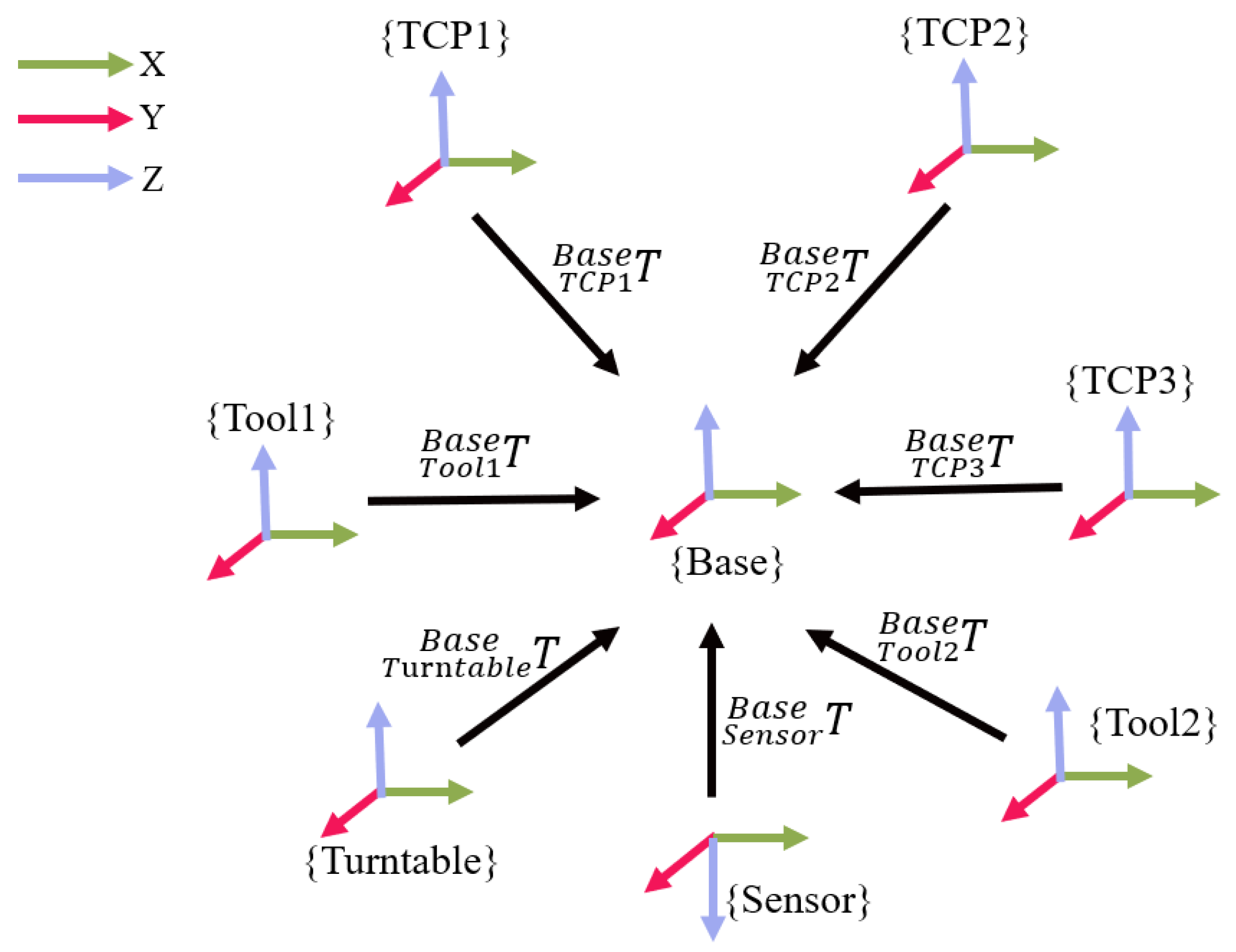
3.6. System Coordinate Unity

The realization of three-dimensional circuit intelligent assembly welding equipment processing tasks, are based on the conversion relationship between the system-related coordinate system. Before the coordinate system calibration, it is necessary to return all axes of motion to zero. The system-related coordinate system schematic is shown in Figure 13 (The coordinate system is represented by pink, blue, and green arrows), where Base represents the machine base coordinate system, TCP1, TCP2, and TCP3, respectively, represent the solder paste spraying end coordinate system, the surface mount resistor end coordinate system, and the laser welding end coordinate system, Tool1 and Tool2, respectively, represent the feeder coordinate system and the solder paste cleaning device coordinate system, Turntable represents the two-dimensional rotary motion module coordinate system, and Sensor represents the point cloud camera coordinate system of the three-dimensional reconstruction mechanism. This equipment adopts the laser tracker for the overall coordinate system calibration, which has the advantages of easy installation, high precision, and real-time tracking, suitable for the coordinate system calibration of this kind of equipment [33].
For each relevant coordinate system, the end coordinate system, tool coordinate system, and rotary table coordinate system can all be calibrated through the translation and rotation movement of the machine tool, but the calibration of point cloud camera coordinate system is the most complex and important. Point cloud camera coordinate system {Sensor} is the image coordinate system of point cloud camera of the three-dimensional reconstruction mechanism, and the obtained processing point coordinates are expressed in this coordinate system. After obtaining the pose of the processing point in the coordinate system of the point cloud camera {Sensor}, hand-eye calibration of the point cloud camera is also required. After calibration, the machining point coordinates and normal vectors can be converted to the reference coordinate system {Base}.
As shown in Figure 6, the point cloud camera is fixed on the 3D reconstruction mechanism; therefore, an auxiliary coordinate system {Temp} is established on the end of visual detection; then, in the actual work process, the conversion relationship between the auxiliary coordinate system and the coordinate system of the point cloud camera is fixed, and the coordinates of the measured point in the base coordinate system can be obtained from Equation (1):
P   B a s e = T T e m p B a s e T S e n s o r T e m p   P   S e n s o r
The calibration process of the point cloud camera is as follows:
(1) First, each movement axis of the machine tool is returned to zero, and the target ball is fixed at any position convenient for measurement at the end of visual detection. The coordinates of the point under the Base coordinate system {Base} are read in the SA software, and are denoted as O1; with the coordinate values X, Y, and Z of O1 as the origin, and the X, Y, and Z axes of the Base coordinate system {Base} as X, Y, and Z axes, the auxiliary coordinate system {Temp} is established, and then:
  T T e m p B a s e   = 1 0 0 0 1 0 0 0 1 X Y Z 0 0 0 1
The X, Y, and Z represent the initial values of the machine tool’s motion axes when they move to the zero point. In the actual work process, it is necessary to add the distance of each movement axis along the X, Y, and Z axis.
(2) Install a calibration plate in a position with a wide field of view, which requires the calibration plate to be within the field of view of the camera. Place another target ball on the target base of standard specifications, and then attach the calibration plate to collect the fitting plane of multiple points, and translate the fitting plane along the normal direction of the plane to the standard height size of the target base to obtain the calibration plate plane.
(3) The machine tool should be controlled to move to a position in front of the calibration plate, which should ensure that the round hole P on the calibration plate is within the range of the point cloud camera. Then, use the hole position of the point cloud camera to identify and determine the coordinate p   S of the round hole on the calibration plate under the point cloud camera coordinate system {Sensor}. The value of O1 at this time was read in the SA software, and the auxiliary coordinate system {Temp} was re-established according to step (1). At the same time, the target ball was placed on the round hole of the calibration plate to collect the point position for several times, and a point was obtained by fitting. The actual position of the hole was projected to the plane of the calibration plate, and the coordinates p   T of the point under the auxiliary coordinate system {Temp} were viewed in the SA software.
(4) Take the coordinate values of point p, respectively, in the point cloud camera coordinate system and the auxiliary coordinate system as a set of data, change the pose of the calibration board, repeat step (3). In order to ensure the accuracy of the calibration, it is necessary to obtain at least 10 groups of data, which are recorded as P   S p   S 1 , p   S 2 , , p   S n and P   T p   T 1 , p   T 2 , , p   T n .
(5) Finally, the conversion relationship between the point cloud camera coordinate system {Sensor} and the auxiliary coordinate system is solved using the obtained data. {Temp}. Since the pose relationship between the auxiliary coordinate system {Temp} and the Base coordinate system {Base} can be measured according to the laser tracker and read directly in the SA software, the hand-eye calibration of the binocular vision camera can be completed via the corresponding coordinate system transformation according to Equation (1). The relevant coordinate system transformation during calibration is shown in Figure 14.
The SVD decomposition method is used to solve the rotation matrix and shift matrix between the point cloud camera coordinate system {Sensor} and the auxiliary coordinate system {Temp}. It should be noted that the coordinate system of the point cloud camera itself is the Cartesian left-hand coordinate system, so it is necessary to pre-process the values of Z coordinates of all points in the system in reverse. After data preprocessing, the specific solution process is as follows:
(1) Solve the center of point set P   S   and P   T :
p   S ¯ = 1 n i = 1 n p   S i p   T ¯ = 1 n i = 1 n p   T i
(2) Decentralize the two-point set:
p   S i = p   S i p   S ¯ p   T i = p   T i p   T ¯
(3) Calculate the covariance matrix H between point sets:
H = i = 1 n p   S i ( p   T i ) T
(4) SVD decomposition of matrix H:
H = U D V T
(5) The rotation matrix R S e n s o r T e m p and the translation matrix t S e n s o r T e m p can be obtained via the following formula:
R S e n s o r T e m p = V U T t S e n s o r T e m p = p   T ¯ R S e n s o r T e m p p   S i ¯
Through the data processing of Formula (3) to Formula (7), the final pose transformation matrix can be solved, the coordinate system calibration of the point cloud camera can be completed, and then the pose information of the processing point can be converted to the Base coordinate system {Base} through Formula (1), which is convenient for subsequent welding paste spraying, resistance mounting, laser welding, and other processes.
After each coordinate system of the intelligent assembly equipment system of the array antenna unit is defined, taking the laser welding process as an example, when welding a certain processing point, there is the following coordinate transformation relationship:
P M B a s e 1 = T S e n s o r B a s e P M S e n s o r 1 = T T C P 1 B a s e P N T C P 1 1 = P N B a s e 1
Where T S e n s o r B a s e and T T C P 1 B a s e represent the homogeneous transformation matrix between point cloud camera coordinate system {Sensor}, solder paste spray end coordinate system {TCP1}, and Base coordinate system {Base}, respectively. P M B a s e and P M S e n s o r represent the coordinate of processing point M in the base coordinate system {Base} and point cloud camera coordinate system {Sensor}, and P N B a s e and P N S e n s o r represent the coordinate of solder paste spray end point N in the Base coordinate system {Base} and point cloud camera coordinate system {TCP1}. The processing point and the laser welding end position are unified in the base coordinate system. The unified relationship of each coordinate system is shown in Figure 15.

4. Simulation and Experiments

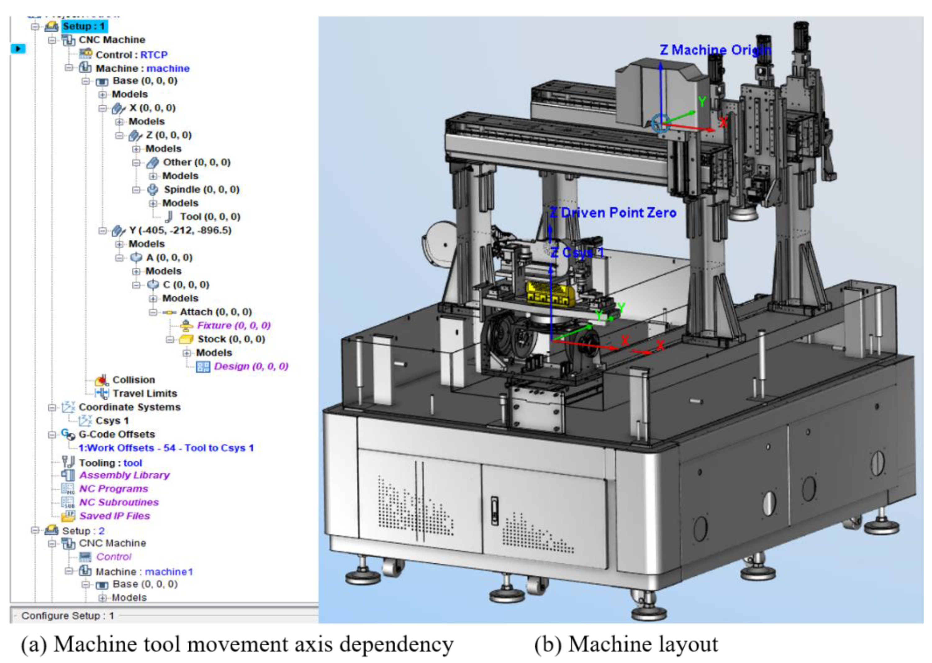
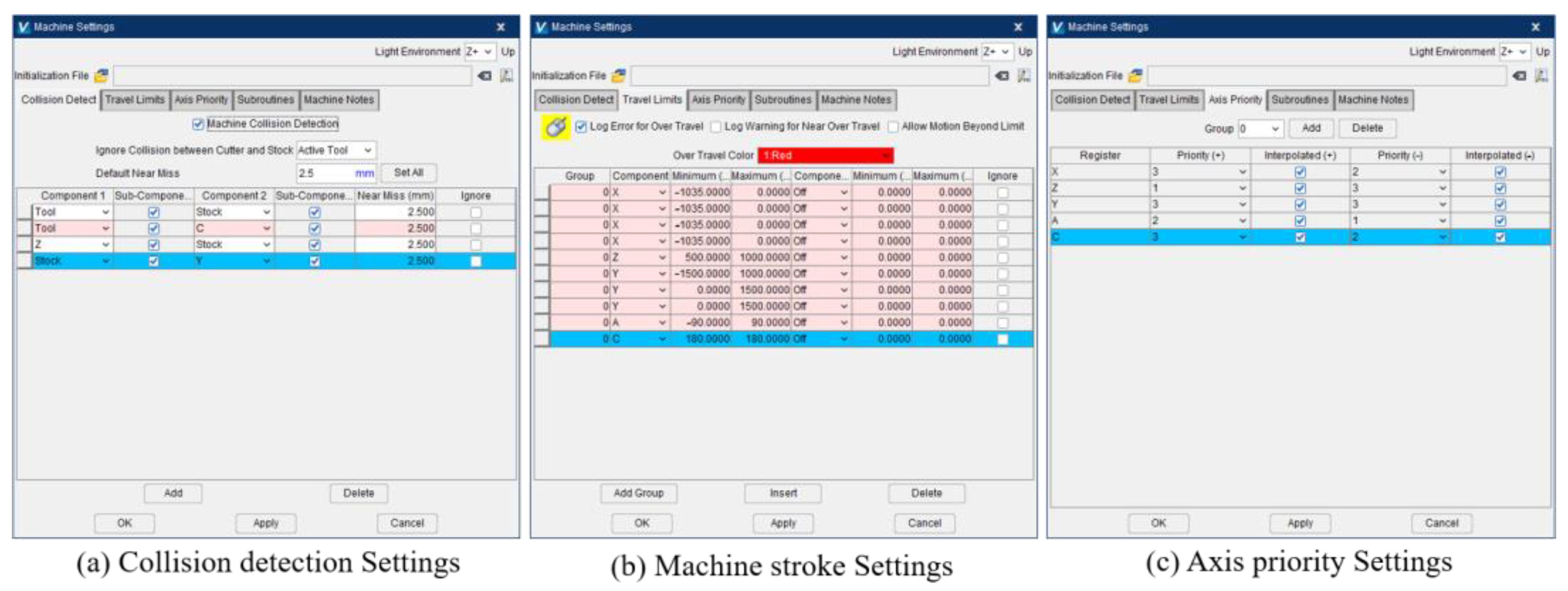
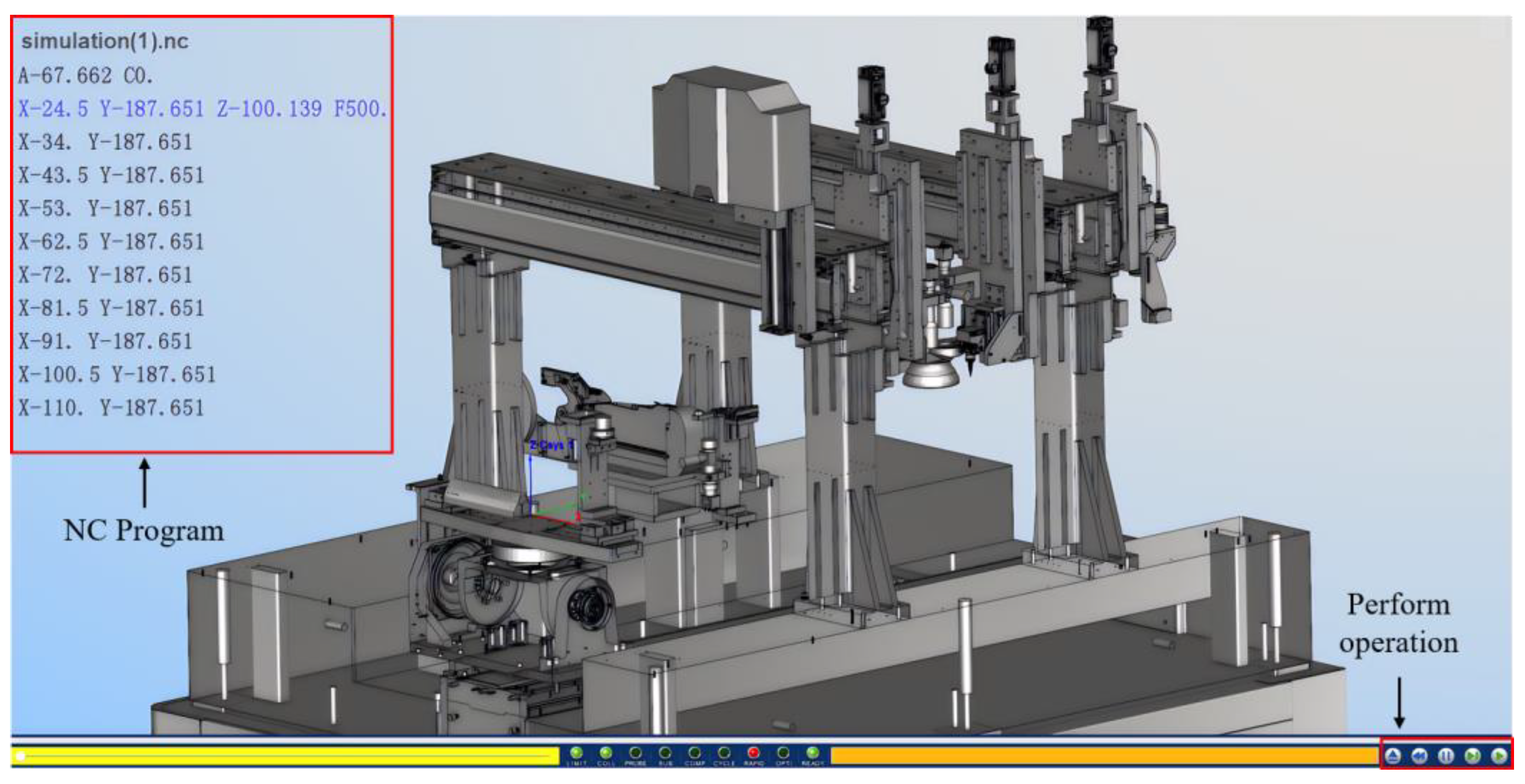
4.1. Machining Motion Simulation Based on Vericut
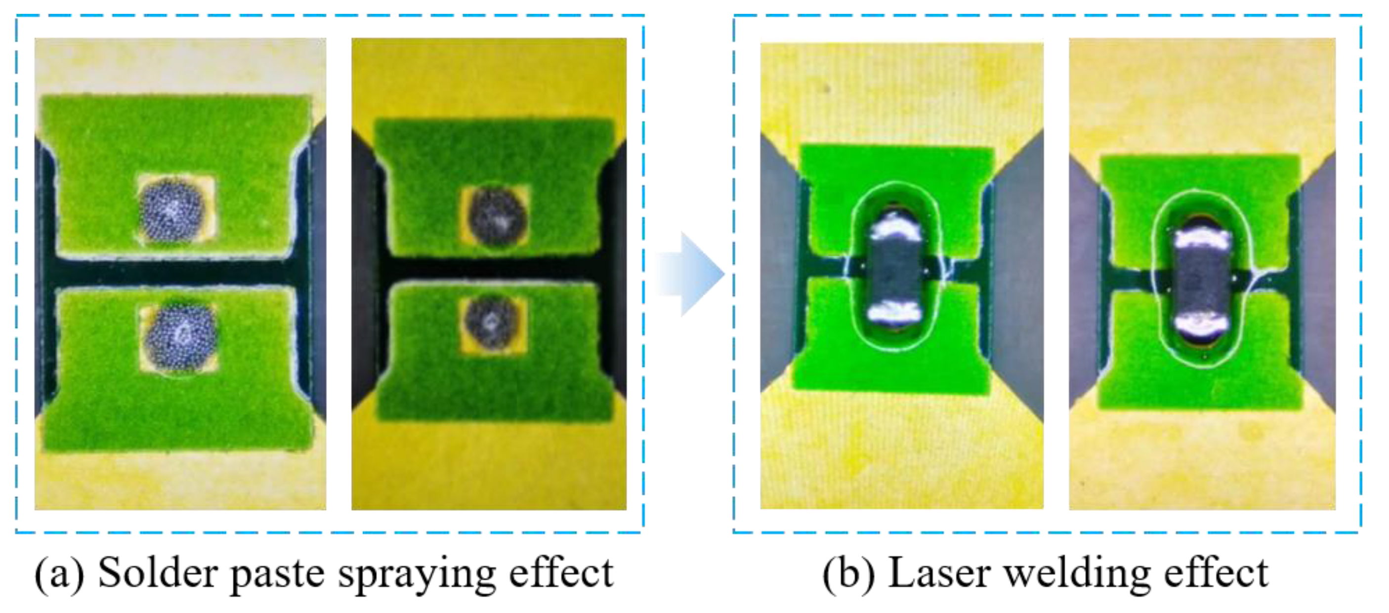
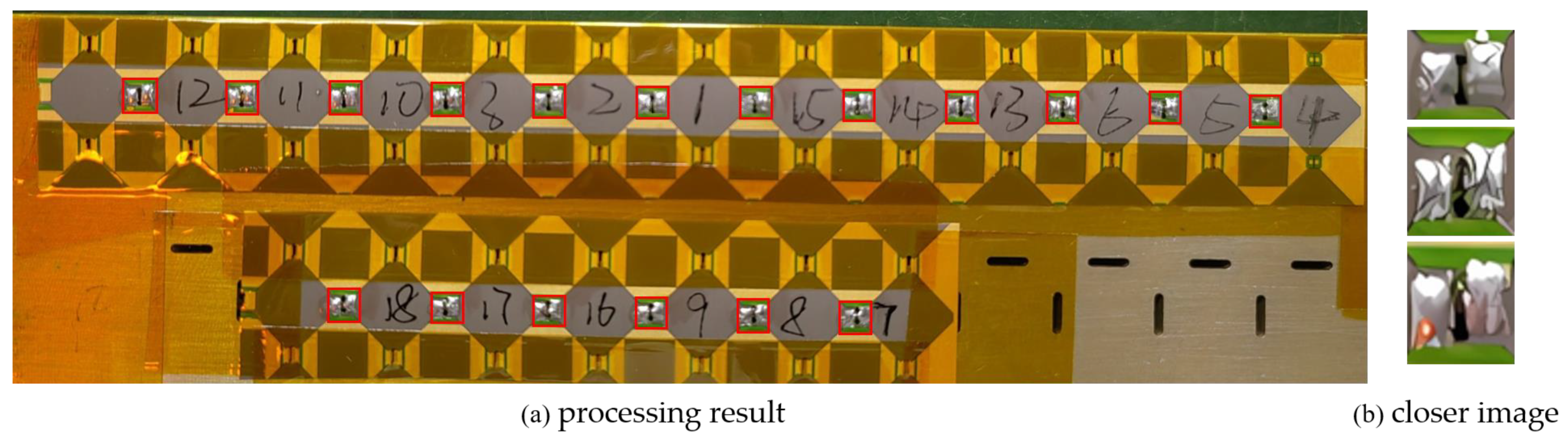
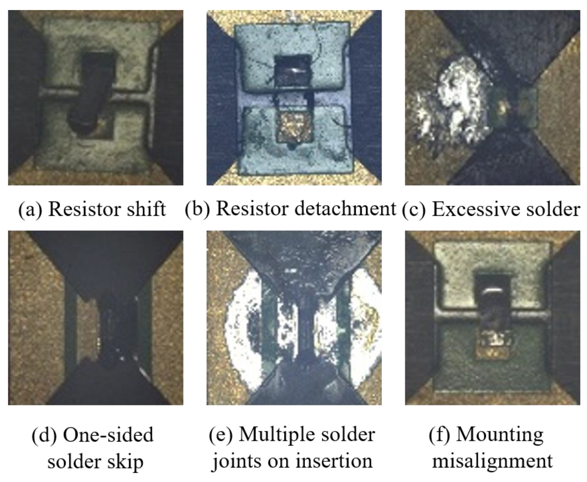
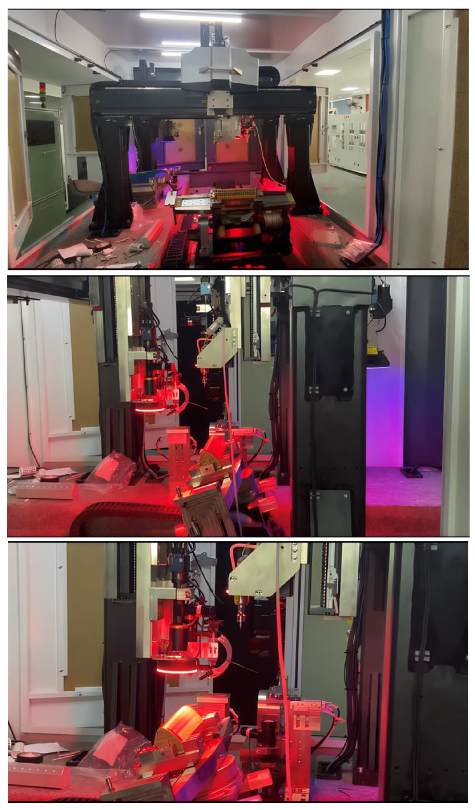
To validate the feasibility and performance of the equipment during the design process, motion simulation based on Vericut was utilized [34]. This simulation enabled the testing of the equipment without the need for physical manufacturing, saving both time and cost. In this section, Vericut software is used for CNC machining simulation. First, a 3D model and machine tool layout are built in Vericut, and the machine tool coordinate system, machining coordinate system, tool coordinate system, etc., are set up, as shown in Figure 16. For ease of observation, the machine tool safety protection shell and external control devices are hidden, and only the moving mechanism and various processing modules are displayed. By setting the direction and relationship of each axis of motion of the machine tool, the machining sequence and range of motion of the moving mechanism are constrained [35,36].
After building the model, auxiliary systems are set up, including collision detection, travel limits, etc. The default setting of the software’s internal system is not to perform collision detection. By setting up collision detection, if the 3D model comes into contact or collides during the motion process, it is considered a collision. The specific configuration is shown in Figure 17.
Based on CAM software, the CNC machining program is generated and imported into the “CNC Program” in the Vericut simulation system. The 3D model follows the machining process according to the CNC program. If there are situations such as overtravel or collision, the system will issue a simulation error alarm, as shown in Figure 18.
Through the Vericut simulation, the accessibility analysis and collision detection of the equipment model were completed, and the generated NC program was verified. By checking the error logs of the simulation, the machining program was modified and optimized. The final simulation results showed that the design layout and coordinate system setting of the entire equipment met the machining range and requirements of the workpiece, and there were no interference or collision situations.

4.2. Experiment

After completing the machining motion simulation, a solid machining experiment was conducted, and overall control of the mechanism was achieved using Huazhong CNC. The workpiece parameters and experimental table parameters used in the experiment are shown in Table 2.
After manual installation of the workpiece, the computer runs the NC program, and the equipment obtains the solder paste spraying data, resistor mounting pressure data, and laser welding data in the process database, which are executed by the end of the modules. The final machining effect is shown in Figure 19. In order to verify whether the processing meets the requirements, combined with machine learning algorithms to train the judgment model, through the post-weld visual inspection to determine the percentage of unprocessed, unqualified processing, lack of welding, and leakage of welding points, the high sensitivity sensor feedback force control accuracy, and the laser interferometer and dial indicator to measure the accuracy of the mechanical movement, the final results of all experiments were analyzed against meeting the processing requirements, and the detailed test results are shown in Table 3. Therefore, the conformal antenna manufactured by the intelligent assembly and welding equipment for three-dimensional integrated circuits can be fully applied to the intelligent assembly of radar electronic equipment, improving the production efficiency of electronic warfare equipment and making a huge contribution to the development of the electronic warfare field.
The traditional processing method relies on manual processing, and the professional ability of the personnel in the actual operation is different. The process of spraying solder paste, mounting resistors, soldering, etc., relies entirely on the professionalism of the processing personnel, which can lead to the quality of the processed product being difficult to guarantee, and there are often processing errors in some positions (as shown in Figure 20), resulting in short circuits or broken circuit, which ultimately cause the entire conformal antenna to stop functioning. Due to the small size of the processing points, in the actual production process, the error rate of manual operation is very high, the processing time of a workpiece is usually more than 24 h, the overall processing efficiency and processing quality is low, and the processing cost is high. Compared with the processing results shown in Figure 19 (Numbers in Figure 19 represents the processing sequence), the equipment proposed in this paper can be a good solution to the problems caused by human error, and under the premise of ensuring quality, the efficiency will be increased by more than 50%, thus reducing production costs and effectively avoiding the problems arising from the “human” factor.
The real picture of the intelligent equipment proposed in this paper is shown in Figure 21, in which can clearly be seen the internal layout of the equipment and the machining status of the workpiece. Even though the machining process is complicated, we have realized the layout of the modules in a reasonable space, and it is almost the same as the model diagram of the equipment shown in the previous section. In order to introduce this equipment in more detail, the technical parameters and specifications of the main modules of this equipment are listed in Table 4.

5. Conclusions

This paper presents an integrated precision manufacturing equipment which can complete the task of intelligent assembly and welding, and has been successfully applied to the three-dimensional circuit machining on the surface of conformal antenna. This article analyzes the difficulties of three-dimensional circuit assembly and processing, and it breaks through the difficulties of three-dimensional circuit processing, such as high personnel dependence, poor processing quality, and poor reliability. The article optimizes the overall processing flow, designs the overall structure of the equipment, verifies the feasibility of the equipment’s mechanical structure based on simulation experiments, builds an experimental platform, and verifies the comprehensive performance of the designed solder paste spraying module, resistor mounting module, and laser welding module. Additionally, the equipment can adapt to more conformal antenna models by changing the fixture form of the two-dimensional rotary motion module, making it highly versatile. The experimental results show that the surface processing point repeat positioning accuracy of the three-dimensional circuit is better than ±30 μm, the mounting force control accuracy of the resistor is better than ±0.1 N, the visual measurement repeat measurement accuracy is less than ±10 μm, and the visual recognition accuracy is higher than 99%. Compared with manual production, the first-pass yield rate reaches 95%, and production efficiency is improved by more than 50%. Finally, the cost and environmental performance of the intelligent processing equipment proposed in this paper are in line with national and industry standards and are suitable for mass production. It is hoped that the research results of this paper can provide certain guidance for the implementation of three-dimensional circuit intelligent processing equipment.

Author Contributions

Conceptualization, W.T., X.D. and C.W.; validation, W.T., X.D. and C.W.; investigation, Z.W., K.L., C.D. and Y.D.; writing—original draft preparation, Z.W., K.L. and Y.D.; writing—review and editing, W.T., X.D. and C.W.; supervision, W.T., X.D., C.W. and W.L.; project administration, X.D. and C.D.; funding acquisition, X.D. and C.D. All authors have read and agreed to the published version of the manuscript.

Funding

This research was funded by the National key R&D program of China (2020YFB1710300) and the National Defense Basic Scientific Research Program of China (No. JCKY2019210B004).

Informed Consent Statement

Not applicable.

Data Availability Statement

Not applicable.

Acknowledgments

The authors would like to acknowledge the financial support from the National key R&D program of China (2020YFB1710300) and the National Defense Basic Scientific Research Program of China (No. JCKY2019210B004).

Conflicts of Interest

The authors declare no conflict of interest.

References

  1. Miqueo, A.; Torralba, M.; Yagüe-Fabra, J.A. Lean manual assembly 4.0: A systematic review. Appl. Sci. 2020, 10, 8555. [Google Scholar] [CrossRef]
  2. Jiang, Z.; Cao, X.; Huang, X.; Li, H.; Ceccarelli, M. Progress and development trend of space intelligent robot technology. Space Sci. Technol. 2022, 2022, 9832053. [Google Scholar] [CrossRef]
  3. Tian, W.; Ding, Y.; Du, X.; Li, K.; Wang, Z.; Wang, C.; Deng, C.; Liao, W. A Review of Intelligent Assembly Technology of Small Electronic Equipment. Micromachines 2023, 14, 1126. [Google Scholar] [CrossRef]
  4. Li, N.; Bu, S.H.; Shang, B.L.; Li, Y.B.; Tang, Z.L.; Zhang, W.W. Aircraft intelligent design: Visions and key technologies. Acta Aeronaut. Et Astronaut. Sin. 2021, 42, 213–230. [Google Scholar]
  5. Liu, H.C.; Yan, X.J.; Hui, H.C. Design of Axis Hole Parts Positioning System Based on Monocular Vision. Mach. Electron. 2021, 39, 70–75. [Google Scholar]
  6. Dolgui, A.; Sgarbossa, F.; Simonetto, M. Design and management of assembly systems 4.0: Systematic literature review and research agenda. Int. J. Prod. Res. 2022, 60, 184–210. [Google Scholar] [CrossRef]
  7. Lei, J.; Yang, J.; Chen, X.; Zhang, Z.; Fu, G.; Hao, Y. Experimental demonstration of conformal phased array antenna via transformation optics. Sci. Rep. 2018, 8, 3807. [Google Scholar] [CrossRef]
  8. Schippers, H.; Verpoorte, J. Overview and Main Achievements of the ACASIAS Project. Schiopers2020 Overview AM. Marknesse: NLR. 2020, pp. 1–2. Available online: http://www.acasias-project.eu/files/Slot2_ACASIAS_overview-achievements.pdf (accessed on 10 August 2023).
  9. Hao, S.; Ma, T.L.; Wang, Y.; Xiang, J.W.; Ma, H.Z.; Jiang, B.F.; Cao, J. Progress and application of key technologies of Sensor Craft. Acta Aeronaut. Astronaut. Sin. 2023, 44, 6–39. [Google Scholar]
  10. Alt, K.H.; Lockyer, A.J.; Coughlin, D.P.; Kudva, J.N.; Tuss, J. Overview of the DoD’s rf multifunction structural aperture (MUSTRAP) program. Proc. SPIE-Int. Soc. Opt. Eng. 2001, 4334, 137–146. [Google Scholar]
  11. Baek, S.M.; Lim, S.J.; Ko, M.G.; Park, M.Y.; Kim, M.S. Structural Design, Fabrication and Static Testing of Smart Composite Skin Structure: Conformal Load-Bearing SATCOM Array Antenna Structure (CLSAAS). Int. J. Aeronaut. Space Sci. 2020, 21, 50–62. [Google Scholar] [CrossRef]
  12. Han, L.; Wang, G.; Jiang, W.X.; Zhao, P.B.; Tang, W.; Liu, T.; Dang, T. Application research on the 3D printing technology in airborne ultra-wideband conformal antenna. Chin. J. Radio Sci 2023, 1–7. Available online: http://kns.cnki.net/kcms/detail/41.1185.TN.20230508.1754.001.html (accessed on 10 August 2023).
  13. Peng, J.; Qu, S.W.; Xia, M.; Yang, S. Wide-Scanning Conformal Phased Array Antenna for UAV Radar Based on Polyimide Film. IEEE Antennas Wirel. Propag. Lett. 2020, 99, 1. [Google Scholar] [CrossRef]
  14. Shi, Z.Y.; Ye, D.; Peng, Z.H.; Xie, H.; Wang, H.Y.; Jiang, Y.; Huang, Y.A. Research progress on novel manufacturing approaches of conformal antenna for aircraft. Acta Aeronaut. Astronaut. Sin. 2021, 42, 157–173. [Google Scholar]
  15. Zhu, J.; Zhou, H.; Wang, C.; Zhou, L.; Yuan, S.; Zhang, W. A review of topology optimization for additive manufacturing: Status and challenges. Chin. J. Aeronaut. 2021, 34, 91–110. [Google Scholar] [CrossRef]
  16. Shin, D.; Sun, C.; Kim, J.H.; Regmi, A.; Chang, J. Direct-Printing of Functional Nanofibers on 3D Surfaces Using Self-Aligning Nanojet in Near-Field Electrospinning. Adv. Mater. Technol. 2020, 5. [Google Scholar] [CrossRef]
  17. Li, Z.; Huang, J.; Yang, Y.; Yang, S.; Zhang, J.; Yuan, P.; Zhang, J. Additive Manufacturing of Conformal Microstrip Antenna Using Piezoelectric Nozzle Array. Appl. Sci. 2020, 10, 3082. [Google Scholar] [CrossRef]
  18. Saada, G.; Layani, M.; Chernevousky, A.; Magdassi, S. Hydro printing conductive patterns onto 3D structures. Adv. Mater. Technol. 2017, 2, 1600289. [Google Scholar] [CrossRef]
  19. Le Borgne, B.; De Sagazan, O.; Crand, S.; Jacques, E.; Harnois, M. Conformal electronics wrapped around daily life objects u-sing an original method: Water transfer printing. ACS Appl. Mater. Interfaces 2017, 9, 29424–29429. [Google Scholar] [CrossRef]
  20. Wu, H.Y.; Chiang, S.W.; Yang, C.; Lin, Z.; Liu, J.; Moon, K.S.; Kang, F.; Li, B.; Wong, C.P. Conformal pad-printing electrically conductive composites onto thermoplastic hemispheres: Toward sustainable fabrication of3-cents volumetric electrically small antennas. PLoS ONE 2015, 10, e0136939. [Google Scholar] [CrossRef]
  21. Purvis, A.; Mcwilliam, R.; Johnson, S.; Seed, N.L.; Williams, G.L.; Maiden, A.; Ivey, P.A. Photolithographic patterning of bihelical tracks onto conical substrates. J. Micro/Nanolithography MEMS MOEMS 2007, 6, 043015. [Google Scholar] [CrossRef]
  22. Jobs, M.; Hjort, K.; Rydberg, A.; Wu, Z. A tunable spherical cap microfluidic electrically small antenna. Small 2013, 9, 3230–3234. [Google Scholar] [CrossRef] [PubMed]
  23. Hu, J.; Li, P.; Dai, H. Mechanical and electric performance characterization of screen printed flexible membrane antennas. J. Harbin Inst. Technol. 2018, 50, 18–23. [Google Scholar]
  24. Li, Y.T. Application analysis of domestic electronic components. China Plant Eng. 2022, 496, 247–248. [Google Scholar]
  25. Wang, C.; Li, P.; Ren, Z.; Meng, F. Effect and experiment of curvature radius of 3-D printed conformal load-bearing antenna array on EM performance. Int. J. RF Microw. Comput.-Aided Eng. 2020, 30, e22130. [Google Scholar] [CrossRef]
  26. Chen, Q.L. Research on Key Technologies of Robot Fine Compliance Assembly. Master’s Thesis, Beijing University of Posts and Telecommunications, Beijing, China, 2019. [Google Scholar]
  27. Zhang, K.; Shi, M.H.; Xu, J.; Liu, F.; Chen, K. Force control for a rigid dual peg-in-hole assembly. Assem. Autom. 2017, 37, 200–207. [Google Scholar] [CrossRef]
  28. Yang, Y.C.; Wang, H.Q.; Liu, Q.P.; Wang, F.Z.; Wang, Z.Y. Research on precision assembly of industrial robot based on force/position hybrid control. Manuf. Autom. 2021, 43, 56–59. [Google Scholar]
  29. Lin, C.J.; Lin, C.H. Using an improved differential evolution for scheduling optimization of dual-gantry multi-head surface-mount placement machine. Mathematics 2021, 9, 2016. [Google Scholar] [CrossRef]
  30. Deng, L.; Wang, L.; Sheng, B.Y.; Xiao, Z. Path planning of automatic optical inspection based on variable neighborhood ant colony algorithm. Comput. Eng. Des. 2020, 41, 354–360. [Google Scholar]
  31. Wei, W.; Li, J.Y.; Wang, H. Path optimization for PCB NC-drilling using genetic algorithm. Comput. Eng. Appl. 2008, 44, 229–232. [Google Scholar]
  32. Xiong, D.J. Research on the Key Technology of Vision Detection of High Precision SMT System. Master’s Thesis, Guangdong University of Technology, Guangzhou, China, 2020. [Google Scholar]
  33. Jin, J.; Tian, W.; Li, B. Design of an Automatic Drilling-riveting End-effector. China Mech. Eng. 2020, 31, 1555–1561. [Google Scholar]
  34. Shi, X.L.; Deng, J.J.; Gai, Y.H.; Zhang, J.W. Simulation Method of Posture Alignment and Docking of Large Aircraft Components Based on DELMIA. Aeronaut. Manuf. Technol. 2020, 63, 24–28. [Google Scholar] [CrossRef]
  35. Sheng, W.S.; Xu, A.P.; Xu, L.J. Simulation of traveling salesman path planning based on ant colony algorithm and genetic algorithm. Comput. Simul. 2022, 39, 398–402+412. [Google Scholar]
  36. Chen, P.; Lei, X.J.; Li, C.; Hu, Y.L.; Chen, S. Assembly of countersunk-hole parts based on 3D pose estimation and impedance. Opt. Precis. Eng. 2022, 30, 2889–2900. [Google Scholar] [CrossRef]
Figure 1. Defense electronic equipment.
Applsci 13 09359 g001
Figure 2. Design and manufacture of conformal antenna [17,25] (reproduced with permission from [17], Wiley, 2019).
Applsci 13 09359 g002
Figure 3. Partial schematic of flexible three-dimensional integrated circuits.
Applsci 13 09359 g003
Figure 4. Variable curvature shape diagram.
Applsci 13 09359 g004
Figure 5. Overall process solution.
Applsci 13 09359 g005
Figure 6. Overall structural model diagram.
Applsci 13 09359 g006
Figure 7. Two-dimensional rotary motion model diagram.
Applsci 13 09359 g007
Figure 8. Three-dimensional reconstruction architecture module diagram.
Applsci 13 09359 g008
Figure 9. Solder paste spraying module diagram.
Applsci 13 09359 g009
Figure 10. Electronic resistor mounting module diagram.
Applsci 13 09359 g010
Figure 11. Laser welding module model diagram.
Applsci 13 09359 g011
Figure 12. Soldering and welding effect images.
Applsci 13 09359 g012
Figure 13. System coordinate system diagram.
Applsci 13 09359 g013
Figure 14. Coordinate system conversion for point cloud camera calibration.
Applsci 13 09359 g014
Figure 15. Coordinate system unified relationship diagram of intelligent assembly welding equipment of three-dimensional circuit.
Applsci 13 09359 g015
Figure 16. Machine initial state.
Applsci 13 09359 g016
Figure 17. Auxiliary system settings.
Applsci 13 09359 g017
Figure 18. Machining simulation.
Applsci 13 09359 g018
Figure 19. Processing result diagram.
Applsci 13 09359 g019
Figure 20. Common processing defects in traditional processing methods (manual processing).
Applsci 13 09359 g020
Figure 21. Real equipment diagram.
Applsci 13 09359 g021
Table 1. Solder paste coating and surface mount welding test parameters.
Process NameProcess Parameters
Solder pasteModel number: YB-B63;
Type 5 powder
Particle size range: 15~25 μm
Solder paste viscosity: 60~200 Pa/s
Solder paste viscosityLeft: 4 mg; right: 4 mg
Air pressure/Dwell time during soldering4 mg–0.2 Mpa/370 ms
Type of dispensing needleDispensing needle: 22 g
Inner diameter: 0.25 mm
Laser welding machine power60 W
Spot diameter1.83 mm
Laser focal length75 mm
Laser temperature modePower upper limit: 40% ± 2; temperature setting: 120 °C/1 s; 165 °C/0.5 s; 230 °C/1 s
Table 2. Solder paste coating and surface mount welding test parameters.
Process NameProcess Parameters
Equipment machining range500 × 300 × 300 mm
Number of machining points18
Size of machining points0.2 × 0.25 mm
Solder paste viscosity60~200 Pa/s
Laser welding power75 W
Resistor mounting pressure3 ± 0.05 N
Table 3. Experimental test results.
Measurement TypeMeasurement DataComparison of Results with Targets
Unprocessed points0Processing points ≥ 99%
Compliance
Missing/leaking welding points0Normal welding points ≥ 99%
Compliance
Force control accuracy±0.03 N<±0.1 N
Compliance
Visual positioning accuracy0.0166 mm<±0.03 mm
Compliance
Welding accuracy±8 μm<±10 μm
Compliance
Table 4. Equipment parameters.
NameTechnical IndicatorsTechnical Parameters
EquipmentEquipment machining range>500 × 300 × 300 mm
Eco-friendly performanceGB16297-1996 <Comprehensive Emission Standards for Air Pollutants> Level 2 Standard
Safety functionFault alarm function, overload, power failure and other protection or alarm function
Two-dimensional rotary motion moduleDriving methodDirect-drive motor
Rotation rangeA: ≥±90°, C: ≥±360°
Position accuracyA ± 10 arc sec
C ± 10 arc sec
Repeated positioning
accuracy
A ± 2.5 arc sec
C ± 2.5 arc sec
Solder paste spraying moduleMinimum diameter of spray point≤250 μm
Single-point accuracy≤±40 μm
Single-point
repeated accuracy
≤±35 μm
Spraying function 1Multiple CAD files converted to spray programs for automatic matching of solder paste volume
Spraying function 2Self-positioning and self-calibration
Solder Paste NozzlesReplaceable and
anti-static
Resistor mounting moduleRange0.3 × 0.6 mm ≈ 3 × 3 mm
SMT precisionIC: 30 μm@3Sigma
Chip: 50 μm@3Sigma
Angular repeated accuracy≤0.05°
Mounting FunctionsConversion of various CAD files to patch programs
Placement force
control range
0.5 ≈ 7 N
Automatic positioning
accuracy for visual
recognition
≤±0.05 mm
Intelligent pressure feedback and control capabilityProgrammable control with intelligent
pressure feedback and intelligent control function
Laser welding moduleLaser welding functionDisplay, edit, save, and recall
process parameters
Temperature control
accuracy
≤±5 °C
Automatic positioning
accuracy for visual
recognition
≤±0.02 mm
Laser irradiation spot size (diameter)The size covers the range of 0.4 mm to 3 mm and is adjustable.
Disclaimer/Publisher’s Note: The statements, opinions and data contained in all publications are solely those of the individual author(s) and contributor(s) and not of MDPI and/or the editor(s). MDPI and/or the editor(s) disclaim responsibility for any injury to people or property resulting from any ideas, methods, instructions or products referred to in the content.

