Article

On-Demand Waveguide-Integrated Microlaser-on-Silicon

Department of Physics, Konkuk University, Seoul 05029, Republic of Korea
*
Author to whom correspondence should be addressed.
These authors contributed equally to this work.
Appl. Sci. 2023, 13(16), 9329; https://doi.org/10.3390/app13169329
Submission received: 25 July 2023 / Revised: 12 August 2023 / Accepted: 15 August 2023 / Published: 17 August 2023
(This article belongs to the Special Issue Advanced Infrared Semiconductor Lasers and Integrated Optics Devices)

Abstract

:
The integration of high-quality III–V light sources on the Si platform has encountered a challenge that demands a highly precise on-demand addressability of single devices in a significantly reduced integration area. However, simple schemes to address the issue without causing major optical losses remain elusive. Here, we propose a waveguide-integrated microlaser-on-silicon in which the III–V/Si integration requires only a small micron-sized post structure with a diameter of <2 µm and enables efficient light coupling with an estimated coupling efficiency of 44.52%. Top-down fabricated high-quality microdisk cavities with an active gain medium were precisely micro-transferred on a small Si-post structure that was rationally designed in the vicinity of a strip-type Si waveguide (WG). Spectroscopic measurements exhibit successful lasing emission with a threshold of 378.0 µW, bi-directional light coupling, and a propagation of >50 µm through the photonic Si WG. Numerical study provides an in-depth understanding of light coupling and verifies the observations in the experiment. We believe that the proposed microlaser-on-Si is a simple and efficient scheme requiring a minimum integration volume smaller than the size of the light source, which is hard to achieve in conventional integration schemes and is readily applicable to various on-demand integrated device applications.

1. Introduction

Optical integration, which was first proposed in 1969, has been extensively studied over the past decades [1,2,3,4,5]. It is defined as the integration of optical components that enable the transmission, modulation, and detection of light on a single chip [6,7,8,9,10,11,12,13,14,15,16,17,18,19,20,21]. Numerous types of integrated devices with various optical functions have been theoretically proposed and experimentally realized using several photonic platform materials including compound semiconductors (InP, GaAs), elementary semiconductors (Si, Ge), silica, and polymers [22,23,24,25,26,27]. In particular, the potential of leveraging the state-of-the-art nanoscale complementary metal-oxide-semiconductor (CMOS) manufacturing technology and superior material properties such as high purity, low defect density, high thermal conductivity, and high refractive index have made Si-based photonic systems the most promising optical integration platform [3,4,5]. Further, Si exhibits almost negligible optical absorption at telecommunication wavelengths and thus already has become a predominant platform for integration. However, despite the substantial progress being made in Si-based light modulation and detection and their large-scale, cost-effective, monolithic device integration technology, the realization of efficient and reliable light sources, such as high-quality lasers on Si, has remained a challenge because of the fundamental limitations of the Si—the phonon-involved slow recombination rate, the enhanced free-carrier absorption (FCA), and the large Auger recombination for high-carrier-injection environments. Two major goals have been pursued simultaneously: the development of high-performance microlasers and their efficient integration into Si platforms [2].
Some strategies using the flip-chip technique and adhesive-polymer-assisted, direct-contact-based and/or oxide-bond-based die-to-wafer bonding combined with special surface treatments as well as template-assisted monolithic integration have enabled the realization of heterogeneous or hybrid integration of III–V compound active semiconductors with passive Si components [6,7,8,9,10,11,12,13,14,15,16,28,29]. Further, they successfully demonstrated the lasing emission and evanescent-type light coupling or hybridized-mode-type laser devices. However, these approaches often involve imprecise manual processes and consequently induce a relatively large initial misalignment, which should later be complementarily compensated with a post-integration III–V device fabrication process, such as photolithography. Thus, to use these approaches, one should initially bond a large volume of III–V dies in an extended area of the coupling region, which inevitably sacrifices the massive III–V materials, high integration density, and compactness [7,10,12]. In this regard, a recently emerging integration technique of micro transfer printing using a microstructured adhesive polymer stamp has drawn considerable attention, demonstrating its ability to mechanically manipulate micro- and nano-scale materials and structures in a highly precise and accurate manner [18,19,20,21,30,31,32,33]. For example, an edge-emitting III–V gain media was transfer-printed using a polymer microtip [17,18]. A bundle of nanoscale semiconductor wires was selectively picked up using a flat-tip polydimethylsiloxane (PDMS) micro-stamp and transferred to a targeted location on a receiving device substrate, thus enabling simultaneous lasing operations at multiple sites [33]. In addition, prefabricated one-dimensional (1D) photonic crystal (PhC) nanocavities with or without a supporting frame structure were successfully transferred, without any damage, onto silicon-on-insulator (SOI) or SiO2 wafers [19,20,34]. However, despite these pioneering works mentioned above as well as the recent development of topological integrations, simple schemes to achieve a further efficient integration that requires a small coupling area have been increasingly demanded [35,36]. Moreover, as more miniaturized and complicated photonic circuits are pursued, it has become of great importance to achieve the on-demand addressability at target locations. In particular, integration without causing significant mechanical damage, optical losses, and/or performance degradation has become critical but remains a challenge [21,30,31].
In this study, we propose a waveguide-integrated microlaser-on-silicon by utilizing a previously developed microtip-assisted transfer-printing method. In the following section, we illustrate a rational design including a microscale Si-post and an on-demand Si-waveguide-integrated microlaser (Section 2.1). Then we describe the important fabrication steps for Si-post structures in the vicinity of strip-type Si waveguides (WGs) and for the separately top-down fabricated arrays of semiconductor microdisks (Section 2.2). The precise alignment transfer of a microdisk on top of a Si-post readily enabled the realization of on-demand WG-coupled microlaser-on-Si integration. Spectroscopic measurements demonstrated the successful lasing emission, light coupling, and propagation through the WG (Section 2.3). The experimental observations were qualitatively verified through numerical simulations (Section 2.4).

2. Results and Discussion

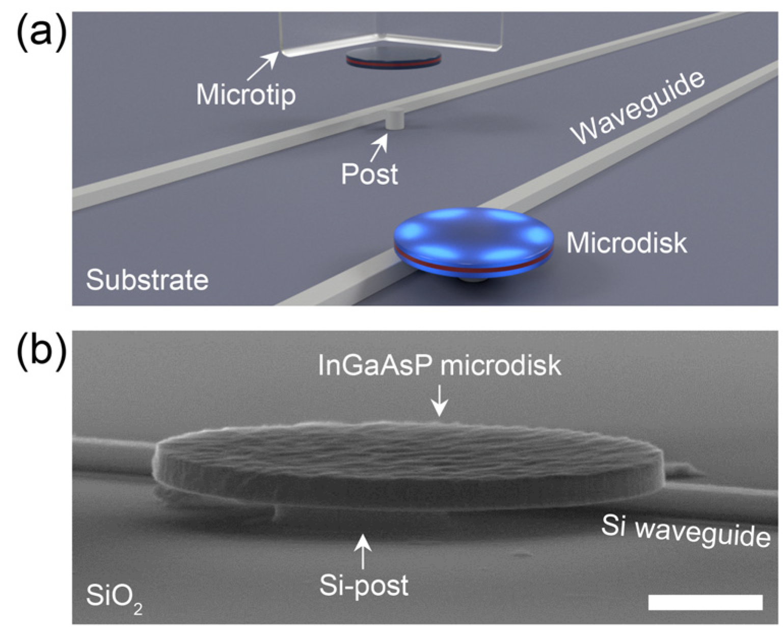
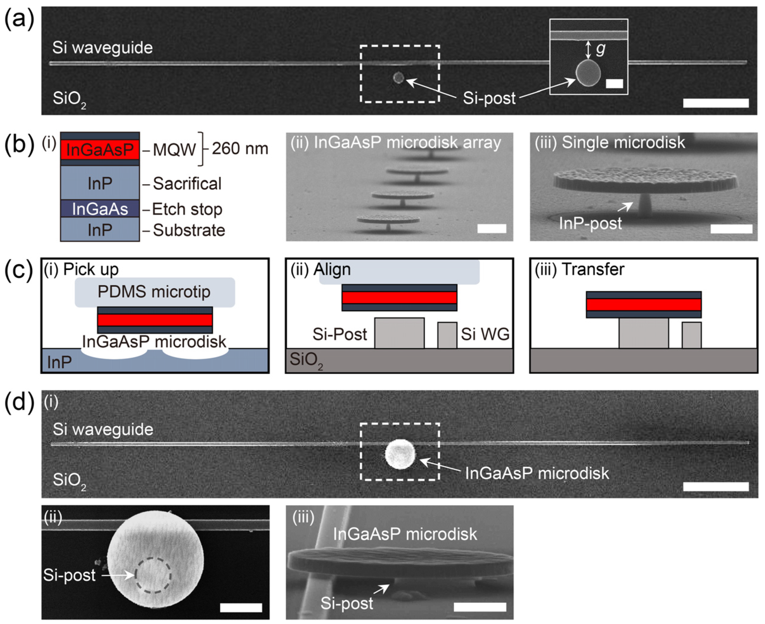
2.1. On-Demand Si-Waveguide-Integrated Microdisk Laser

Figure 1a depicts a schematic of the proposed microdisk laser transferred onto a small Si-post and integrated with a strip-type Si WG. The III–V semiconductor microdisk includes an optical gain medium and represents a high-index active optical microcavity that supports resonant whispering gallery modes (WGMs). The Si-post and WG structures were rationally designed to achieve an efficient light coupling when the light source was integrated. Thereafter, the PDMS transfer-printing technique was used for a highly accurate and damage-free transfer of a microdisk onto a target Si-post, which readily enables the realization of on-demand microlaser-on-Si. Figure 1b depicts a tilted-view scanning electron microscopy (SEM) image of a fully fabricated WG-integrated laser device. The InGaAsP microdisk with a diameter of approximately 4.5 µm and thickness of 260 nm was transferred onto a Si-post with a size of approximately 1.6 µm. The multi-quantum-well (MQW) structure with a central emission wavelength of approximately 1.5 µm was introduced in the middle of the microdisk, where it served as an optical gain medium. When integrated, the Si-post supported the central part of the microdisk such that the boundary of the microdisk, where the WGMs are typically formed, could be air-suspended. This high-index contrast helps in strong field confinement, and thus enables the successful excitation of high-quality-factor (Q-factor) resonant modes.

2.2. Device Fabrication

Figure 2 depicts the device fabrication process. First, we used an SOI wafer with a 260 nm thick Si device layer and a 3.0 µm thick SiO2 layer to fabricate the arrays of Si-posts and strip-type Si WGs with different widths, lengths, and gap distances. These arrays were readily patterned in a deterministic manner using either electron beam lithography (EBL) or photolithography. The conventional dry-etching technique (CCP-RIE) and a few rounds of O2-plasma treatment completed the passive device fabrication. As per the requirements, another round of dry etching was briefly introduced to the Si WG to slightly reduce the height of the WG with respect to that of the Si-post. Importantly, when the microdisk was transferred onto the post, this height difference induced a small air gap between the bottom of the microdisk and the top of the WG, which allowed the evanescent coupling of the light. Thus, the light transmission through the waveguide could be controlled by systematically controlling the air gap. Figure 2a depicts a representative SEM image of the fabricated Si-post and WG. The width and length of the Si WG were approximately 500 nm and approximately 105.8 μm, and the size of Si-post was approximately 1.6 μm in diameter, respectively. The small post was designed to firmly support the entire microdisk structure but minimally perturb the resonant modes. The gap between the post and the WG was approximately 1.1 μm (inset, Figure 2a). In this device, we designed the Si-post to be located in the middle of the longitudinal Si WG to examine how accurately we could integrate the laser device and achieve equal light couplings toward the right and left directions.
The microdisks were fabricated using a 260 nm thick InGaAsP slab containing six InGaAs/InGaAsP quantum-wells (QWs). Underneath the slab, a 900 nm thick InP sacrificial layer was introduced for the selective chemical etching, which readily enabled the microdisks to be air-suspended at the boundaries and post-supported at the center ((i), Figure 2b). Thereafter, we used the EBL to define arrays of microdisks of different sizes, which were mechanically dry-etched using chemically assisted ion beam etching (CAIBE). After removing the residual resist using O2-plasma treatments, time-sensitive anisotropic chemical etching (HCl:DI = 3:1) was applied to produce a submicron-sized post structure ((ii), Figure 2b). In particular, an effort was made to keep the post size smaller than approximately 400 nm to facilitate the pick-up and separation process. Panel (iii) of Figure 2b depicts the fabricated single InGaAsP microdisk with a supporting InP-post of size of approximately 280 nm.
The schematics in Figure 2c illustrate the key steps involved in the on-demand laser-on-Si integration. We used a previously developed PDMS microtip-assisted transfer printing technique to pick up the fabricated single microdisk on the InP substrate ((i)), move it to a receiving Si device substrate ((ii)), and align-transfer it on a target Si-post ((iii)) [21,30,31]. A PDMS stamp with a 20 × 20 × 20 μm3 cubical microtip was surface-treated under the UV radiation with an illumination power of 10.4 mW/cm for 60 s to control the adhesive energy [37].
The low- and high-magnification SEM images depicted in Figure 2d show the top and tilt views of the Si WG-integrated microlaser-on-Si device. The transferred microdisk laser was slightly off-centered at approximately 700 nm with respect to the center of the Si-post. Consequently, the upper boundary of the microdisk, which was originally designed to be aligned with the underlying Si WG, was shifted upward by the same misalignment ((ii), Figure 2d). It should be noted that this misalignment inevitably occurs during the micro transfer printing owing to the limited imaging resolution of the optical microscope system and the finite precision of manual manipulation. An extensive study on misalignment, including the statistical results for different sizes of Si-posts, can be found in Ref. [30]. The high-magnification tilt-view SEM image reveals the details of the coupling geometry ((iii), Figure 2d). As anticipated, the boundary of the microdisk was air-suspended, and a nanoscale air gap between the microdisk and the Si WG, typically a few tens of nanometers, was clearly observed. Notably, this air gap can be controllably increased or decreased by selectively depositing materials on top of the Si-post (e.g., SiO2, resist polymers) or additionally dry-etching the Si WG in the coupling region.

2.3. Optical Characterizations

We systematically performed micro-photoluminescence (PL) spectroscopy to investigate the optical properties of the integrated microdisk laser and the light coupling and propagation through the WG. The fabricated device, depicted in Figure 2d, was mounted on an XYZ stage and optically pumped at room temperature using a pulsed laser diode with a wavelength of 976 nm. Incident pulses with a width of 100 ns at a repetition rate of 1 MHz were used. Light emitted from the device was collected using a 50× microscope objective with a numerical aperture of 0.42 and sent to an infrared (IR) camera for imaging or a monochromator for spectroscopic analysis. We note that the collection of maximum light intensities can be further optimized by using an objective lens with high numerical aperture and different magnification. First, we gradually increased the peak pump power (Ppeak) and imaged the light emission from the laser device. The captured IR camera images depicted in Figure 3a exhibit the spontaneous (i), amplified spontaneous (ii), and lasing (iii) emission patterns, respectively. Light intensities in all panels were normalized to the maximum value of panel (iii). In particular, we observed nearly uniform light emissions from the entire body of microdisk at Ppeak = 301.8 μW but stronger light intensities from the boundary than those from the center at Ppeak = 398.8 μW. This clearly indicates that the excitation of resonant WGMs and the corresponding amplification of spontaneous emission developed at a Ppeak between the two pump powers. At further increased Ppeak = 497.6 μW, a clearer donut-shaped intensity distribution with a strong light interference pattern, which is a typical profile of resonant WGMs, was observed. This indicated the successful lasing operation in the device. We also noted that the slight misalignment in the micro-transfer process might contribute little to the lasing oscillations; thus, the result demonstrated the transfer tolerance in our device design.
For the quantitative characterization, we measured the lasing spectra with increasing Ppeak. The characteristic light-in versus light-out curve exhibited a superlinear increase in intensity with a threshold peak pump power (Pth) of approximately 378.0 μW ((i), Figure 3b). The peak power per unit area of approximately 30.1 μW/μm2 falls within the range of typically accepted incident power for micro-resonators, which often allows some intriguing nonlinear phenomena such as optical bistability [38]. As anticipated, the measured threshold was larger than the Ppeak of panel (i) but smaller than that of panel (ii) of Figure 3a, thus strongly supporting the observations and analysis depicted in Figure 3a. In addition, we plotted the linewidth (∆λ1/2) ((ii), Figure 3b) and peak wavelength (λLaser) of lasing spectra as a function of Ppeak ((iii), Figure 3b). From these data, the experimental Q-factors (λ/∆λ1/2) were estimated as > 2300 at near threshold, which is comparable to those reported in previous study [30]. A typical linewidth reduction and blue shift of the peak wavelength were observed from below- to near-threshold regimes. Interestingly, an abrupt linewidth broadening from 0.64 nm to 0.67 nm near Ppeak = 497.6 μW was observed and its plateau clamped at 0.68 nm afterward. In addition, the lasing peak was noticeably red shifted by 0.07 nm near Ppeak = 497.6 μW and remained a constant for the increased Ppeak. We believe that these unusual observations can be partly explained by the steady-state stimulated light coupling to the WG, which is discussed in a later section.
Next, to examine how the light from the laser efficiently couples to the Si WG, we repeatedly imaged the light scattered at both ends of the WG while increasing Ppeak from below- to above-threshold. Figure 3c exhibits captured IR camera images of the scattered light at both terminations of WG (left and right panels) and the light emission from the laser device (middle panel) at different Ppeak of 398.8 μW (i) (near-threshold) and 497.6 μW (ii) (above-threshold), respectively. At below-threshold, no noticeable light scattering is observed. However, evident light spots were observed at both terminations for Ppeak > Pth, indicating successful light coupling and transmission toward both directions. For the qualitative analysis, we first compared the recorded maximum light intensities from single pixels at the WG end (Ileft or Iright) with that of the laser (Idisk) at Ppeak = 398.8 μW, and the ratios of WG left end (Ileft/Idisk) and WG right end (Iright/Idisk) to the laser were approximately 0.21 and 0.22, respectively ((i), Figure 3c). This discrepancy in the intensity ratios can be attributed to unequal light coupling from the clockwise (CW) and counterclockwise (CCW) WGMs to the propagating WG modes, which originated from the uneven and off-center-transferred microdisk. In addition, this ratio difference became more evident with an increasing Ppeak. For example, the measured Ileft/Idisk and Iright/Idisk ratios are approximately 0.35 and 0.31 at Ppeak = 497.6 μW, respectively ((ii), Figure 3c). Moreover, the ratios of the same WG end at different Ppeak values exhibit noticeable variations. Based on these observations, we hypothesized that besides the light coupling from the laser mode to the fundamental WG mode (kWG), there should be a small portion of spontaneous emission that coupled to several higher-order WG modes. Significantly, the transmitted power carried by the fundamental WG mode thus varies in response to laser power at Ppeak > Pth, whereas the transmitted powers carried by other WG modes might remain constant. This can partly explain the total intensity ratio that eventually converges to the ratio associated with the light coupling of the stimulated emission alone at high Ppeak.
For the spectroscopic study, we measured the spectra from the selected area, including each WG end ((i) left, (iii) right, Figure 3c) and the laser center ((ii), Figure 3c). The intensities of the spectra were normalized to the peak values shown in panel (ii). As anticipated, the normalized peak intensity ratios of the left-(Ipeak,left/Ipeak,disk) and right-end of WG (Ipeak,right/Ipeak,disk) were measured as approximately 0.34 and approximately 0.27, respectively, which agrees well with the previous results from Figure 3c. The high-resolution spectra (right insets, Figure 3d) reveal how the light couplings were established in the left and right directions of the WG. For example, compared to the spectrum from the disk center (inset of (ii)), the spectrum from the left WG (right inset of (i)) exhibits an almost identical peak shape to the major laser peak at 1496.71 nm (rightward arrow) but a partial suppression of the minor shoulder peak at 1495.71 nm (downward arrow). In contrast, the spectrum from the right WG (right inset of (iii)) reveals significant suppression of the minor shoulder peak (downward) as well as the major laser peak (rightward). In particular, the considerably high intensities for wavelengths longer than the peak reveal how much light coupling in the right direction was limited compared to that in the left direction. Furthermore, angle-resolved spectroscopy showed linear polarization of the scattered light at both WG ends (left insets of (i) and (iii), Figure 3d), revealing the transverse electric (TE)-polarized nature of the WG modes (kWG, Figure 3c).

2.4. Numerical Simulations

Three-dimensional (3D) finite-difference time-domain (FDTD) simulations were performed to obtain an in-depth understanding of light coupling. Figure 4a depicts the index profiles of the top and side views of the simulated structure. For a direct comparison with the study, we used structural parameters similar to those of the fabricated device, as shown in Figure 2d. As in the experiment, the InGaAsP microdisk was slightly misaligned by 700 nm with respect to the center of the Si-post and was in the longitudinal center of the 100-μm-long Si WG.
To excite the resonant WGMs, an electric dipole with a wavelength of 1501 nm was introduced in the microdisk. Along the WG, we set a series of monitoring planes perpendicular to the axis of the WG ((i), Figure 4a), which included the cross-section of the Si WG on the SiO2 substrate ((ii), Figure 4c). Then the total power emitted from the microdisk (Outdisk) and the transmitted power passing through the monitor planes (TWG) were calculated. Furthermore, we introduced additional monitoring planes at positions 270 and 570 nm above the microdisk and WG, respectively, to calculate the vertical component of the emitted powers from the microdisk (Topdisk) and WG ends (TopWG) ((ii), Figure 4a). Figure 4b depicts the calculated electric field intensity distributions at the center of the microdisk (i) and Si WG (ii) (white dotted lines of the inset in Figure 4a), exhibiting a strongly confined WGM within the microdisk and coupled light propagation through the WG ((ii), Figure 4b). To estimate the light-coupling efficiency (ηc), we plotted the normalized transmitted power (TWG/Outdisk) as a function of the monitoring position ((i), Figure 4c). Then, the data obtained from positions ranging from 3–48 μm were linear-fitted to exclude the power directly from the microdisk. The extrapolated value on the y-axis represents the coupling efficiency (ηc), which was estimated to be approximately 44.52%. In addition, we calculated the y-component of the electric fields of the propagating TE-like WG mode at a 40 μm distant detection position. The field profile revealed that the light from the microdisk was coupled to the fundamental WG mode ((iii), Figure 4c). Finally, we calculated the normalized power in the vertical direction (TopWG/Topdisk) at both ends and directly compared them with those from the experiment (IWG/Idisk), as shown in Figure 4d. Despite the minor discrepancy in values, the results qualitatively show good agreement between the simulation and experiment, demonstrating the on-demand addressability of our micro-transfer-printing technique.

3. Conclusions

In conclusion, we demonstrated an on-demand WG-integrated microlaser-on-Si. We designed and fabricated a small Si-post structure in the longitudinal center of a long strip-type Si WG. A top-down fabricated InGaAsP MQW microdisk laser was align-transferred on top of the Si-post and integrated with the Si WG. Optical experiments were carried out and the results exhibited a successful lasing oscillation with a threshold pump power of 378 μW and the light coupling and propagation through the WG. The measured scattered power at the left (Ileft/Idisk) and right WG ends (Iright/Idisk), which were normalized to the emission power of the microlaser, was approximately 35.29% and 30.59%, respectively. The numerical simulation results show a calculated coupling efficiency (ηc) of approximately 44.52%. Despite the small discrepancy in the values, the normalized emitted power at one end of the WG (TopWG/Topdisk) of approximately 38.09% exhibited good qualitative agreement with the experimental results. We believe that our on-demand WG-integrated microlaser-on-Si can be a powerful solution for high-quality light sources in high-density ultracompact photonic integrated circuits and further fulfill important functionality such as high-sensitivity optical sensing [3,4,39]. Furthermore, the proposed integration technique is universally applicable and can thus help the realization of integrated micro- and/or nanoscale optical devices operating at different frequencies.

4. Methods

4.1. Optical Measurement

The PL measurement setup was used for the measurement. A laser diode with a wavelength of 976 nm was connected to a function generator (RIGOL (Beijing, China), DG4162) to generate a pulse wave (pulse width of 100 ns, duty cycle of 5%). The mirrors and 50× microscope objective lens (Mitutoyo (Kawasaki, Japan), M Plan Apo) with a numerical aperture of 0.42 were used to focus the pump beam on the sample attached to the XYZ translation stage (Newport (Irvine, CA, USA), M-562-XYZ). The light emitted from the device was collected with a 50× microscope objective lens and entered an IR camera (Hamamatsu (Hamamatsu, Japan), C12741-03) or a monochromator (Spectral product DK480) with 1200 g/mm grating through mirrors to analyze an image or spectrum. An InGaAs photodetector (Thorlabs (Newton, NJ, USA), PDF10C/M) was used to detect the optical signals.

4.2. Numerical Simulations

We employed a 3D FDTD method (Lumerical (Pittsburgh, PA, USA), FDTD solutions) to support our analysis and experimental results. We first investigated the modal characteristics of the microdisk on the Si-post without Si WG. Further, the light coupling and waveguide characteristics of the real structure were simulated by introducing an Ey electric dipole at the boundary of the light source.

Author Contributions

Conceptualization, B.-J.M. and Y.-S.N.; methodology, B.-J.M.; software, Y.-J.K.; validation, B.-J.M., Y.-J.K. and Y.-S.N.; formal analysis, Y.-J.K. and Y.-S.N.; investigation, B.-J.M., Y.-J.K. and Y.-S.N.; resources, Y.-S.N.; data curation, B.-J.M. and Y.-J.K.; writing—original draft preparation, B.-J.M. and Y.-S.N.; writing—review and editing, Y.-S.N.; visualization, B.-J.M.; supervision, Y.-S.N.; project administration, Y.-S.N.; funding acquisition, Y.-S.N. All authors have read and agreed to the published version of the manuscript.

Funding

Y.-S.N. acknowledges the support from the National Research Foundation of Korea (NRF) grant funded by the Korean government (2018R1C1B3001130). This research was supported by the Korea Basic Science Institute (National research Facilities and Equipment Center) grant funded by the Ministry of Education (2022R1A6C101A754).

Institutional Review Board Statement

Not applicable.

Informed Consent Statement

Not applicable.

Data Availability Statement

Not applicable.

Acknowledgments

We thank Min-Woo Kim and Sun-Wook Park at Konkuk University for the help with device fabrication.

Conflicts of Interest

The authors declare no conflict of interest.

References

  1. Miller, S.E. Integrated Optics: An Introduction. Bell Syst. Tech. J. 1969, 48, 2059–2069. [Google Scholar] [CrossRef]
  2. Liang, D.; Bowers, J.E. Recent progress in lasers on silicon. Nat. Photonics 2010, 4, 511–517. [Google Scholar] [CrossRef]
  3. Soref, R. The past, present, and future of silicon photonics. IEEE J. Sel. Top. Quantum Electron. 2006, 12, 1678–1687. [Google Scholar] [CrossRef]
  4. Smit, M.; Leijtens, X.; Ambrosius, H.; Bente, E.; Van der Tol, J.; Smalbrugge, B.; De Vries, T.; Geluk, E.J.; Bolk, J.; Van Veldhoven, R.; et al. An introduction to InP-based generic integration technology. Semicond. Sci. Technol. 2014, 29, 083001. [Google Scholar] [CrossRef]
  5. Feng, L.; Zhang, M.; Wang, J.; Zhou, X.; Qiang, X.; Guo, G.; Ren, X. Silicon Photonic Devices for Scalable Quantum Information Applications. Photonics Res. 2022, 10, A135–A153. [Google Scholar] [CrossRef]
  6. Tanaka, S.; Jeong, S.-H.; Sekiguchi, S.; Kurahashi, T.; Tanaka, Y.; Morito, K. High-output-power, single-wavelength silicon hybrid laser using precise flip-chip bonding technology. Opt. Express 2012, 20, 28057–28069. [Google Scholar] [CrossRef]
  7. Roelkens, G.; Campenhout, J.V.; Brouckaert, J.; Thourhout, D.V.; Baets, R.; Rojo Romeo, P.; Regreny, P.; Kazmierczak, A.; Seassal, C.; Letartre, X.; et al. III-V/Si photonics by die-to-wafer bonding. Mater. Today 2007, 10, 36–43. [Google Scholar] [CrossRef]
  8. Sheng, Z.; Liu, L.; Brouckaert, J.; He, S.; Van Thourhout, D. InGaAs PIN Photodetectors Integrated on Silicon-on-Insulator Waveguides. Opt. Express 2010, 18, 1756–1761. [Google Scholar] [CrossRef]
  9. Roelkens, G.; Van Thourhout, D.; Baets, R.; Nötzel, R.; Smit, M. Laser emission and photodetection in an InP/InGaAsP layer integrated on and coupled to a Silicon-on-Insulator waveguide circuit. Opt. Express 2006, 14, 8154–8159. [Google Scholar] [CrossRef]
  10. Campenhout, J.V.; Rojo-Romeo, P.; Regreny, P.; Seassal, C.; Thourhout, D.V.; Verstuyft, S.; Cioccio, L.D.; Fedeli, J.-M.; Lagahe, C.; Baets, R. Electrically pumped InP-based microdisk lasers integrated with a nanophotonic silicon-on-insulator waveguide circuit. Opt. Express 2007, 15, 6744–6749. [Google Scholar] [CrossRef]
  11. Karle, T.J.; Halioua, Y.; Raineri, F.; Monnier, P.; Braive, R.; Gratiet, L.L.; Beaudoin, G.; Sagnes, I.; Roelkens, G.; Laere, F.V.; et al. Heterogenous integration and precise alignment of InP-based photonic crystal lasers to complementary metal-oxide semiconductor fabricated silicon-on-insulator wire waveguides. J. Appl. Phys. 2010, 107, 063103. [Google Scholar] [CrossRef]
  12. Fang, A.W.; Park, H.; Cohen, O.; Jones, R.; Paniccia, M.J.; Bowers, J.E. Electrically pumped hybrid AlGaInAs-silicon evanescent laser. Opt. Express 2006, 14, 9203–9210. [Google Scholar] [CrossRef]
  13. Liang, D.; Fiorentino, M.; Okumura, T.; Chang, H.-H.; Spencer, D.T.; Kuo, Y.-H.; Fang, A.W.; Dai, D.; Beausoleil, R.G.; Bowers, J.E. Electrically-pumped Compact Hybrid Silicon Microring Lasers for Optical Interconnects. Opt. Express 2009, 17, 20355–20364. [Google Scholar] [CrossRef] [PubMed]
  14. Liang, D.; Huang, X.; Kurczveil, G.; Fiorentino, M.; Beausoleil, R.G. Integrated finely tunable microring laser on silicon. Nat. Photonics 2016, 10, 719–722. [Google Scholar] [CrossRef]
  15. Crosnier, G.; Sanchez, D.; Bouchoule, S.; Monnier, P.; Beaudoin, G.; Sagnes, I.; Raj, R.; Raineri, F. Hybrid Indium Phosphide-on-Silicon Nanolaser Diode. Nat. Photonics 2017, 11, 297–300. [Google Scholar] [CrossRef]
  16. Hattori, H.T.; Seassal, C.; Touraille, E.; Rojo-Romeo, P.; Letartre, X.; Hollinger, G.; Viktorovitch, P.; Di Cioccio, L.; Zussy, M.; Melhaoui, L.E.; et al. Heterogeneous integration of microdisk lasers on silicon strip waveguides for optical interconnects. IEEE Photonics Technol. Lett. 2006, 18, 223–225. [Google Scholar] [CrossRef]
  17. Billah, M.R.; Blaicher, M.; Hoose, T.; Dietrich, P.-I.; Marin-Palomo, P.; Lindenmann, N.; Nesic, A.; Hofmann, A.; Troppenz, U.; Moehrle, M.; et al. Hybrid integration of silicon photonics circuits and InP lasers by photonic wire bonding. Optica 2018, 5, 876–883. [Google Scholar] [CrossRef]
  18. Roelkens, G.; Zhang, J.; Bogaert, L.; Billet, M.; Wang, D.; Pan, B.; Kruckel, C.J.; Soltanian, E.; Maes, D.; Vanackere, T.; et al. Micro-Transfer Printing for Heterogeneous Si Photonic Integrated Circuits. IEEE J. Sel. Top. Quantum Electron. 2023, 29, 8200414. [Google Scholar] [CrossRef]
  19. Karnadi, I.; Son, J.; Kim, J.Y.; Jang, H.; Lee, S.; Kim, K.S.; Min, B.; Lee, Y.H. A printed nanobeam laser on a SiO2/Si substrate for low-threshold continuous-wave operation. Opt. Express 2014, 22, 12115–12121. [Google Scholar] [CrossRef]
  20. Lee, J.; Karnadi, I.; Kim, J.T.; Lee, Y.-H.; Kim, M.-K. Printed Nanolaser on Silicon. ACS Photonics 2017, 4, 2117–2123. [Google Scholar] [CrossRef]
  21. Kim, M.-W.; Park, S.-W.; Park, K.-T.; Min, B.-J.; Ku, J.-H.; Ko, J.-Y.; Choi, J.S.; No, Y.-S. All-Graphene-Contact Electrically Pumped On-Demand Transferrable Nanowire Source. Nano Lett. 2022, 22, 1316–1323. [Google Scholar] [CrossRef] [PubMed]
  22. Huber, T.; Predojević, A.; Khoshnegar, M.; Dalacu, D.; Poole, P.J.; Majedi, H.; Weihs, G. Polarization Entangled Photons from Quantum Dots Embedded in Nanowires. Nano Lett. 2014, 14, 7107–7114. [Google Scholar] [CrossRef] [PubMed]
  23. Huffaker, D.L.; Park, G.; Zou, Z.; Shchekin, O.B.; Deppe, D.G. 1.3 μm room-temperature GaAs-based quantum-dot laser. Appl. Phys. Lett. 1998, 73, 2564–2566. [Google Scholar] [CrossRef]
  24. Liu, A.; Jones, R.; Liao, L.; Samara-Rubio, D.; Rubin, D.; Cohen, O.; Nicolaescu, R.; Paniccia, M. A high-speed silicon optical modulator based on a metal–oxide–semiconductor capacitor. Nature 2004, 427, 615. [Google Scholar] [CrossRef]
  25. Michel, J.; Liu, J.L.; Kimerling, L.C. High-performance Ge-on-Si photodetectors. Nat. Photonics 2010, 4, 527–534. [Google Scholar] [CrossRef]
  26. Knight, J.C.; Birks, T.A.; Russell, P.S.J.; Atkin, D.M. All-silica single-mode optical fiber with photonic crystal cladding. Opt. Lett. 1996, 21, 1547–1549. [Google Scholar] [CrossRef] [PubMed]
  27. Ma, H.; Jen, A.K.-Y.; Dalton, L.R. Polymer-Based Optical Waveguides: Materials, Processing, and Devices. Adv. Mater. 2002, 14, 1339–1365. [Google Scholar] [CrossRef]
  28. Chan, K.C.; Teo, M.; Zhong, Z.W. Characterization of low-k benzocyclobutene dielectric thin film. Microelectron. Int. 2003, 20, 11–22. [Google Scholar] [CrossRef]
  29. Mauthe, S.; Vico Triviño, N.; Sousa, M.; Staudinger, P.; Baumgartner, Y.; Tiwari, P.; Stöferle, T.; Caimi, D.; Scherrer, M.; Schmid, H.; et al. Monolithic integration of III-V microdisk lasers on silicon. In Proceedings of the 2019 International Conference on Optical MEMS and Nanophotonics (OMN), Daejeon, Republic of Korea, 28 July–1 August 2019; pp. 32–33. [Google Scholar]
  30. Park, S.-W.; Kim, M.-W.; Park, K.-T.; Ku, J.-H.; No, Y.-S. On-Chip Transferrable Microdisk Lasers. ACS Photonics 2020, 7, 3313–3320. [Google Scholar] [CrossRef]
  31. Min, B.-J.; Kim, Y.-J.; Choi, J.-H.; Kim, M.-W.; Park, K.-T.; Jang, D.J.; Choi, J.S.; No, Y.-S. Electrically driven on-chip transferrable micro-LEDs. Appl. Phys. Lett. 2022, 121, 241107. [Google Scholar] [CrossRef]
  32. Kim, Y.; Park, B.J.; Kim, M.; Song, D.I.; Lee, J.; Yu, A.; Kim, M.-K. Hybrid Silicon Microlasers with Gain Patches of Unlimited Designs. ACS Photonics 2021, 8, 2590–2597. [Google Scholar] [CrossRef]
  33. Guilhabert, B.; Hurtado, A.; Jevtics, D.; Gao, Q.; Tan, H.H.; Jagadish, C.; Dawson, M.D. Transfer Printing of Semiconductor Nanowires with Lasing Emission for Controllable Nanophotonic Device Fabrication. ACS Nano 2016, 10, 3951–3958. [Google Scholar] [CrossRef] [PubMed]
  34. Osada, A.; Ota, Y.; Katsumi, R.; Watanabe, K.; Iwamoto, S.; Arakawa, Y. Transfer-printed quantum-dot nanolasers on a silicon photonic circuit. Appl. Phys. Express 2018, 11, 072002. [Google Scholar] [CrossRef]
  35. Liu, Q.; Li, S.; Wang, B.; Ke, S.; Qin, C.; Wang, K.; Liu, W.; Gao, D.; Berini, P.; Lu, P. Efficient mode transfer on a compact silicon chip by encircling moving exceptional points. Phy. Rev. Lett. 2020, 124, 153903. [Google Scholar] [CrossRef]
  36. Liu, Q.; Wang, T.; Lei, Q.; Zhao, D.; Ke, S. Nonreciprocal topological mode conversion by encircling an exceptional point in dynamic waveguides. Opt. Lett. 2023, 48, 4089–4092. [Google Scholar] [CrossRef] [PubMed]
  37. Berdichevsky, Y.; Khandurina, J.; Guttman, A.; Lo, Y.-H. UV/ozone modification of poly (dimethylsiloxane) microfluidic channels. Sens. Actuators B Chem. 2004, 97, 402–408. [Google Scholar] [CrossRef]
  38. Mao, C.; Zhong, D.; Liu, F.; Wang, L.; Zhao, D. Multiple optical bistabilities in graphene arrays-bulk dielectric composites. Opt. Laser Technol. 2022, 154, 108292. [Google Scholar] [CrossRef]
  39. Zheng, Y.; Wu, Z.; Shum, P.P.; Xu, Z.; Keiser, G.; Humbert, G.; Zhang, H.; Zeng, S.; Dinh, X.Q. Sensing and lasing applications of whispering gallery mode microresonators. Opto-Electron. Adv. 2018, 1, 180015. [Google Scholar] [CrossRef]
Figure 1. On-demand WG-integrated microlaser-on-silicon. (a) Schematic of the device. A high-index microdisk cavity (dark blue color) with an optical gain medium (red color) is transferred onto a target post and coupled with a strip-type WG using the microtip-assisted transfer-printing technique. (b) Tilted-view SEM image of the fully fabricated WG-integrated laser-on-silicon device. A MQW InGaAsP microdisk with a diameter of approximately 4.5 µm was on-demand transferred on top of a Si-post and coupled to a Si WG. Scale bar: 1 μm.
Applsci 13 09329 g001
Figure 2. Fabrication processes for the on-demand WG-integrated microlaser-on-silicon. (a) SEM images of fabricated strip-type Si WG and Si-post. Inset: high-magnification SEM image showing the Si-post with a diameter of approximately 1.6 μm. The post is located in the longitudinal center of the Si WG with a width of approximately 500 nm and length of approximately 105.8 μm. The gap size between them was approximately 1.1 μm. Scale bar: 10 μm and 1 μm (inset). (b) Fabrication of InGaAsP microdisks. (i) Epitaxial InGaAsP/InP wafer design. (ii) Low-magnification SEM image showing an array of microdisks after the CAIBE and selective chemical etching. (iii) High-magnification tilt-view SEM image showing single microdisk with submicron-sized InP-post structure. The diameter and thickness of the InGaAsP microdisk were approximately 4.5 μm and 260 nm. Scale bar: 1 μm. (c) The PDMS micro-transfer-printing process. (i) Pick-up and separation of single microdisk from the InP substrate. (ii) Locating and coarse alignment with a target Si-post on SOI device wafer. (iii) Center-to-center align-transfer. (d) Si WG-integrated microlaser-on-Si. (i) Low-magnification top-view SEM image of fabricated device. Scale bar: 10 μm. (ii), (iii) High-magnification top- (ii), and tilt-view. (iii) SEM images showing the integration region (white dotted box of (i)). (ii) Transferred microdisk with misalignment of approximately 700 nm. Gray dotted circle indicates the Si-post. Scale bar: 2 μm (iii). Evanescently coupled microdisk and WG with an air gap size of approximately 40 nm. Scale bar: 1 μm.
Applsci 13 09329 g002
Figure 3. Optical characterization. (a) The emission patterns of the laser captured by an IR camera at different Ppeak values of (i) 301.8 μW, (ii) 398.8 μW, and (iii) 497.6 μW. Intensities were normalized with the maximum value of panel (iii). Scale bar: 5 μm. (b) Laser characterization. (i) Light-in versus light-out curve. The threshold power, Pth, was estimated to be approximately 378.0 μW. Laser peak linewidth (ii) and wavelength (iii) plotted as a function of Ppeak. (c) Captured IR camera images showing the scattered light intensities at WG ends (left, right) and the laser emission (middle) at (i) Ppeak = 398.8 μW, (ii) Ppeak = 497.6 μW. The intensities at the ends of the WG were increased by three-fold for comparison. Scale bar: 10 μm. (d) Measured spectra from the left (i) and right ends of WG (iii) and the microdisk center (ii) at Ppeak = 497.6 μW, respectively. The right insets of all panels were high resolution spectra. The left insets of (i) and (iii) were the angle-resolved intensity distributions.
Applsci 13 09329 g003
Figure 4. Numerical simulation of light coupling and propagation. (a) Index profiles of the simulated structures. Top-(i), and side-view (ii) of the Si WG-integrated microdisk. The diameter and thickness of the microdisk (Si-post) were 4.51 μm (1.55 μm) and 260 nm (300 nm), respectively. The width, thickness, and length of Si WG were 470 nm, 260 nm, and 100 μm, respectively. Outdisk and TWG indicate the total power emitted from the microdisks and the transmitted power through the WG. Topdisk and TopWG indicate the vertical component of emitted power from the microdisk and of scattered power at WG end, respectively. Scale bars: 10 μm and 1 μm for (i) and inset of (ii). (b) Calculated electric field intensity distributions at the center of microdisk (i) and WG (ii) (white dotted lines of inset of (a)). (c) Light coupling analysis. (i) Normalized transmitted power (TWG/Outdisk) as a function of distance from the center of WG. (ii) Schematic of WG cross section. Scale bar: 200 nm. (iii) Ey-component of electric fields of the fundamental propagating WG mode. (d) Comparison of simulation and experiment: TopWG/Topdisk (simulation), versus IWG/Idisk (experiment).
Applsci 13 09329 g004
Disclaimer/Publisher’s Note: The statements, opinions and data contained in all publications are solely those of the individual author(s) and contributor(s) and not of MDPI and/or the editor(s). MDPI and/or the editor(s) disclaim responsibility for any injury to people or property resulting from any ideas, methods, instructions or products referred to in the content.

