Review

Optical Beamforming Networks for Millimeter-Wave Wireless Communications

Huawei Technologies Co., Ltd., Shenzhen 518000, China
*
Author to whom correspondence should be addressed.
Appl. Sci. 2023, 13(14), 8346; https://doi.org/10.3390/app13148346
Submission received: 15 May 2023 / Revised: 20 June 2023 / Accepted: 28 June 2023 / Published: 19 July 2023

Abstract

:
With the rapid data growth driven by smart phone, high-definition television and virtual reality/augmented reality devices and so on, the launched 5G and upcoming 6G wireless communications tend to utilize millimeter wave (mmWave) to achieve broad bandwidth. In order to compensate for the high propagation loss in mmWave wireless communications and track the moving users, beamforming and beamsteering are indispensable enabling technologies. These have promising potential to be realized through the use of optical beamforming networks (OBFNs) that have a wider bandwidth and smaller size, lower power consumption, and lower loss compared to those of their electric counterparts. In this paper, we systematically review various OBFN architectures using true time delays and optical phase shifters, as well as discuss performances of different architectures, scalable technologies that promote the advancement of OBFNs, and the application potentials of OBFNs. Two-dimensional OBFNs with discrete components or integrated optical devices have been elaborated, in addition to one-dimensional architectures. Moreover, the state-of-the-art technologies relative to reducing the size, loss and nonlinearity of OBFNs have also been discussed here.

1. Introduction

In the era of 5G and beyond, wireless communications will witness an explosive growth in data traffic with the technology advancements of 4 k/8 k high-definition video, virtual reality/augmented reality (VR/AR), mixed reality (MR), industrial internet of things, remote healthcare and so on [1,2,3,4]. These corresponding application scenarios will drive the evolution of mobile broadband networks toward wide bandwidth and high frequency. To this end, mmWave and terahertz (THz), which have a much larger bandwidth and energy efficiency compared to those of sub-6 GHz, are proposed as the signal carriers of next-generation wireless communication networks [4,5,6,7,8]. Among them, mmWave has gained more popularity in terms of research and application in the past two decades [1,7,8]. However, it is challenging to exploit mmWave, which suffers severe propagation loss in wireless communications, due to the air absorption, rain attenuation and blockages of buildings, foliage and vehicles, etc. [5,7,9]. One key enabling technology for mmWave communications is the phase array antenna (PAA) that adopts a large number of antenna elements to provide sufficient gain in a certain direction through beamforming, and also has the beamsteering ability to track moving users such as pedestrians and passengers in vehicles [8,10,11].
Conventionally, the beamforming and beamsteering of PAAs are implemented using electric beamforming networks that have analog and digital architectures. Analog architectures of electric beamforming generally utilize a phase shifter array that has a bulky size and narrow bandwidth, inducing a high cost and the beam squint problem [12,13]. Meanwhile, digital beamforming networks require that the numbers of high-speed digital–analog converters (ADCs), analog–digital converters (DACs) and mixers are identical to those of antenna elements, which are too expensive to implement in PAAs with massive antenna elements [9,14]. These issues hinder the utilization of electric beamforming networks in mmWave communications with broad bandwidth and compact antenna arrays. One promising solution is to use OBFNs that have inherent advantages in enabling broadband wireless communications, thanks to the wide bandwidth of optical devices and multi-dimensional multiplexing capability of optical signals. With photonic integration technology, OBFNs also possess the potential advantages of small size, low weight, low power consumption and low loss [1,14,15].
OBFNs are used to phase tune or induce a time delay in the radio frequency (RF) signal at each antenna element with optical phase shifters or true time delay (TTD) components, and further control the beam pattern of PAAs. The implementations of OBFNs in PAAs can be dated back to the 1970s [16,17]. Early demonstrations of OBFNs are mainly based on TTD architectures which adopt discrete devices to build fiber-optic or free-space beamforming systems [18,19,20,21]. These architectures are easy to be realized by using commercially mature components; however, their bulkiness inhibits their integration with antennas especially in mmWave wireless communications. OBFNs with optical phase shifters predominantly produce RF signals via coherent beating at photodetectors (PDs), which have a relatively small tuning range and bandwidth [16,22,23,24,25]. Moreover, OBFN architectures combining TTDs and phase shifters have also been demonstrated to have superiorities in reducing the cost and complexity of TTD architectures designed for PAAs with limited bandwidth [20,21]. In recent years, OBFNs with integrated TTDs or integrated phase shifters have received much concern and exhibited advantages in compactness, high scalability and low power consumption [26,27,28,29,30,31]. Several application scenarios of OBFNs such as indoor coverage and mobile fronthaul have been proposed [29,32,33,34,35,36,37,38]. Up to now, reviews about OBFNs have paid more attention on TTD architectures [8,12,15,20,21,39], but the roles and advancements of phase shifter architectures have not been discussed. Furthermore, relative advancements in materials, optical devices and electro-photonic integrations, which may improve the scalability of OBFNs, have not been discussed either.
In this paper, we present a systematic review of OBFN architectures using various TTDs and phase shifters, introduce typical architectures, discuss the scalability of different architectures, as well as propose several scalable techniques and application scenarios for OBFNs. The following sections are organized as follows: Section 2 shows the principles of PAAs, OBFNs with TTDs and phase shifter arrays, Section 3 introduces the representative architectures of five subclasses of OBFNs with TTDs and the corresponding two-dimensional (2D) schemes, Section 4 presents four classic categories of OBFNs with phase shifters and a promising combination of these with TTD architectures, Section 5 discusses the scalability, scalable techniques and application potential of OBFNs in next-generation wireless communication networks, and finally, Section 6 gives the conclusion and outlook.

2. Principles

To sweep the beam in free space for wireless communications, PAAs tune the phase or induce a time delay at each antenna element. For PAAs using OBFNs, the working principles relate to the beam pattern of one-dimensional (1D) and two-dimensional (2D) PAAs, as well as the RF signal processing of OBFNs. The beam pattern is formed by the integral of the electromagnetic field of each antenna in free space. Categorized by the delay, OBFNs have two types: TTD architectures and phase shifter architectures [20]. The former produce different time delays for RF signals transmitted or received by different antenna elements, while the latter produce various phase shifts.

2.1. Beam Pattern of PAAs

PAAs using OBFNs consist of a 1D antenna array or a 2D antenna array and corresponding OBFNs, as shown in Figure 1a,b. For a 1D PAA with equal amplitude and equal spacing (d) between adjacent antennas, the beam pattern (array factor) can be expressed as follows: [40]
F θ = n = 1 N e i ( n 1 ) ( k d s i n θ Δ ϕ )
where Δϕ is the progressive phase of the linear array antenna, k is the wave number of the RF signal exited from the antennas, and θ is the beam angle. The beam angle (θ) can be given as Equation (2) which is derived from F(θ) obtaining the maximum value.
θ = arcsin ( Δ ϕ k d )
Owing to k = 2π/λRF, where λRF is the wavelength of the RF signal, Equation (2) can also be expressed as follows:
θ = arcsin ( Δ ϕ 2 π d λ R F )
Meanwhile, for 2D M × N PAA with equal amplitude and equal spacing (d) between adjacent antenna elements, the beam pattern can be expressed as follows: [40]
F θ ,   φ   = m = 1 M n = 1 N I m n e i ( ( m 1 ) ( k d s i n θ c o s φ ) + ( n 1 ) ( k d s i n θ s i n φ ) )
where θ′ and φ are the azimuthal angle and polar angle in the spherical coordinate system, respectively, and Imn is the excitation of antenna element at m-th row and n-th column.

2.2. Principle of TTD Architectures

As presented in Figure 2, TTD architectures utilize the direct detection of modulated optical carriers, in which the signal processing of a channel is as follows. The optical carrier from a laser is modulated by a RF signal, which is then delayed by a TTD with a time delay of Δt, then the optical carrier is fed to PD and mixed back to RF signal. The other channels have a similar operation with the optical carrier and generate a group of RF signals with a fixed phase difference, in order to form a beam with a certain angle.
Ignoring the high-order harmonics, the optical signal before the PD can be expressed as follows: [30]
S t 1 = A 1 e x p i 2 π f 1 ( t + Δ t ) + A 2 e x p i 2 π f 1 + f R F t + Δ t + ϕ 0 A 2 e x p i 2 π f 1 f R F t + Δ t + ϕ 0
where A1 and A2 are the amplitude of the optical carrier and sidebands, Δt is the time delay, and ϕ0 is the initial phase of the RF signal. Detected by the PD, an electric current is produced as follows:
I t 1 = R S t 1 × S * t 1
where R is the responsivity of PD. Neglecting components of the direct current and beating term, the electric current can be written as follows:
I t 1 = R [ 4 A 1 A 2 cos 2 π f R F ( t + Δ t ) + ϕ 0 ]
This equation states that the phase of the RF signal is shifted by 2πfRFΔt.

2.3. Principle of Phase Shifter Architectures

Typically, the signal processing of phase shifter architectures is characterized by the heterodyne detection of coherent optical carriers. For example, two coherent optical carriers can be produced by two phase-locked lasers, respectively, as plotted in Figure 3. The first optical carrier from one laser is modulated by an electrical signal (RF1), and then the phases of the optical carrier and its modulation sidebands are shifted by the phase shifter or TTD; next, the optical carrier and one sideband are filtered out. The second optical carrier goes directly to the PD and combines with one sideband of the first optical carrier, generating a new electrical signal (RF2) via coherent beating. If the lower sideband of the first optical carrier is left behind, the optical signals before the PD can be expressed as follows:
S t 2 = A 3 e x p i 2 π f 1 f R F 1 t + ϕ + A 4 e x p i 2 π f 2 t
where A3 and A4 are the amplitude of the sideband signal and the second optical carrier. Meanwhile, ignoring the components of direct current and high-order frequency, the electric current can be simplified as follows:
I t 2 = R × [ 2 A 3 A 4 cos 2 π ( f 2 f 1 + f R F 1 ) t ϕ ]
This equation demonstrates that the phase shift in the optical domain can be transferred to one in the RF domain via heterodyne detection which can also change the frequency of the RF signal into a new frequency of fRF2 = f2f1 + fRF1. Derived from Equation (3), the relationship of the phase difference (Δϕ) between adjacent antennas with the beam angle (θ0) is expressed by the following equation.
Δϕ = 2πdsin(θ0)/λRF

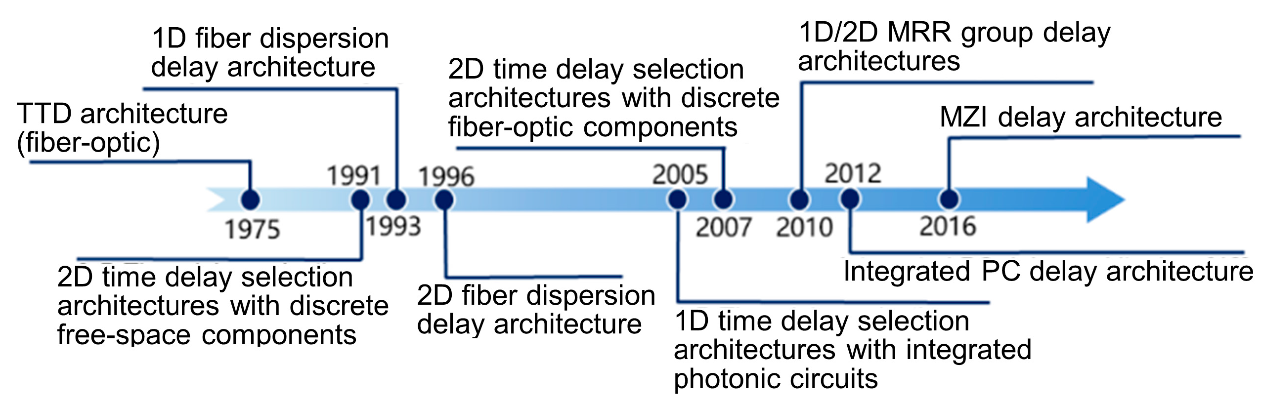
3. OBFNs with TTD Architectures

TTD architectures have the advantages of no beam squint and a large delay tuning range [8,20,41]. As addressed above, OBFNs with TTD architectures can be based on fiber-optic or free-space beamforming systems. Meanwhile, TTD architectures with integrated photonic circuits have also been proposed and demonstrated with the advancement of photonic integration technology, as shown in Figure 4 [17,18,23,24,42,43,44,45,46,47,48,49,50]. It is also shown in this figure that the 1D and 2D OBFN architectures have been proposed since the 1990s. Up to now, TTD architectures mainly include fiber dispersion delay architectures, microring resonator (MRR) group delay architectures, Mach–Zehnder interferometer (MZI) delay architectures, photonic crystal (PC) delay architectures and time delay selection architectures, which will be elaborated in subsequent sections.

3.1. Fiber Dispersion Delay Architectures

The fiber dispersion delay architectures are the most mature ones in TTD architectures, owing to adopting commercially mature fibers and devices. The time delay difference between adjacent beam angles or adjacent channels is produced by the chromatic dispersion of different wavelengths and can be given by the following [43,51]:
Δτ = LD(λ2λ1)
where D is the chromatic dispersion coefficient (ps/nm/km), L is the length of the fiber (km), and λ1 and λ2 represent the adjacent wavelengths (nm).
As shown in Figure 5a,b, the fiber dispersion delay architecture with N channels (equal to the number of antennas) can be established by one tunable laser, one electro-optic modulator, 1 × N splitter, N different fiber delay lines and N PDs, namely the 1λ × N framework [42], while it can also be built by N tunable lasers, one multiplexer, one electro-optic modulator, one fiber, one de-multiplexer and N PDs, namely the × N framework [52]. The 1λ × N framework uses one tunable laser and N fiber channels with different lengths of dispersive fibers and non-dispersive fibers, causing progressive time delays for adjacent antenna elements, whereas the × N framework use only one dispersive fiber, such as a common single-mode fiber (SMF), to afford various delays for N channels. These frameworks realize 1D beam sweeping by changing the laser wavelength, which has the advantage of wide bandwidth that is only limited by the bandwidth (~100 GHz) of optical devices such as modulators and PDs [53,54]. Moreover, the × N framework can achieve very low loss, due to the low transmission loss of commercial SMFs. This advantage can also be obtained in the 1λ × N framework if SMFs with different lengths are utilized in this architecture, instead of using relatively high-loss dispersion fibers. Although the × N framework can largely reduce the cost of the fiber, the increase in number of the tunable laser may be counter-productive in terms of the cost of whole system. Nevertheless, the wavelength multiplexing applied in the × N framework is one of paramount advantages in OBFNs compared to electrical beamforming networks. Note that, a PAA with a large number of antenna elements needs high-resolution scanning with a wide coverage, which further demands a tunable laser with very high tuning precision. For example, as calculated by Equation (12) [52], where n is the bit number corresponding to the resolution of the PAA, a PAA with a six-bit scanning resolution and a RF of 30 GHz requires a tunable laser with a wavelength resolution of less than 10 p.m.
Δλ = 1/(2n+1LDfRF)
For practical implementation, 2D beamforming is a basic requirement for 2D planar PAAs, which can exhibit the superiority of OBFNs thanks to their multi-dimensional multiplexing abilities such as wavelength multiplexing and spatial multiplexing. As illustrated in Figure 6a, an OBFN architecture for 2D PAAs has been proposed [51], using an optical frequency comb, fiber dispersion unit, programmable optical filter and microwave photonic filter (MPF) to control the delay of each channel. The optical frequency comb can simultaneously produce multiple optical carriers with various wavelengths and replace multiple lasers presented in the × N framework, reducing the size of OBFNs. In this architecture, multiple optical carriers are first modulated with N RF frequencies at the polarization modulator (PolM), then delayed by the fiber dispersion unit and selected by the programmable filter which induces N optical carriers to N different MPF paths; finally, RF signals with N center frequencies are generated at MPF paths and sent to an antenna element. This indicates that a 2D PAA with this OBFN architecture can achieve multi-beam beamforming, which is a promising technique for a mmWave massive multiple-input multiple-output (MIMO) system [9,55]. However, there is an issue for this concept in that multi-frequency beamforming requires wideband PAAs which are not commercially available presently. Two-dimensional beamforming with one center frequency is easier to be implemented with a fiber dispersion delay architecture, as shown in Figure 6b [56]. Similarly, an electro-optic frequency comb is utilized to provide multiple wavelengths, whereas optical carriers are modulated by Mach–Zehnder modulators (MZM), are then delayed by two-stage TTDs including dispersion compensation fibers (DCFs) and tunable delay lines (TDLs), and are split into various cores of the multi-core fiber (MCF). Next, they are filtered by de-multiplexers and detected by PDs. Finally, the RF signals produced are distributed to different columns and rows of the PAA. The delays of optical carriers with different wavelengths are separately tuned by DCFs, while relative signal delays in various cores of fiber are controlled by TDLs. This architecture features a time delay variation of less than 1 ps with a drift in room temperature, which is much more stable than that (~15 ps) with a single-mode fiber. Similarly, the 2D OBFN with fiber dispersion delay architectures has a large size and high sensitivity to changes in the environment, since discrete devices and fibers are applied in this architecture.

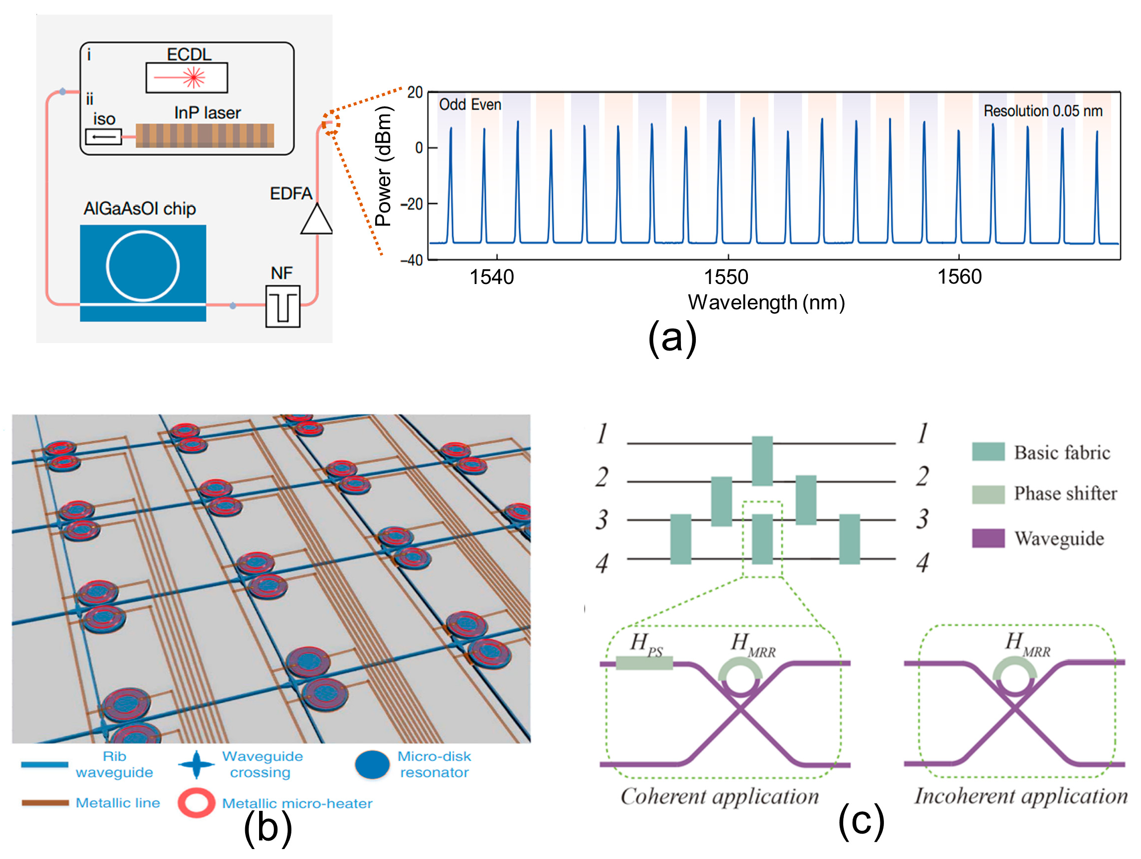
3.2. MRR Group Delay Architectures

With photonic integration technology, a large number of TTDs can be integrated on one substrate, which greatly reduces the size of OBFNs. The MRR group delay architecture, employing multiple MRRs as TTDs, is one approach of such OBFNs within a relatively wide bandwidth, which is typically several gigahertz [26,47,57]. Figure 7a plots the structure of the MRR, which comprises one microring and one bus waveguide. The time delays of a MRR with a round-trip time of 20 ps (free spectral range = 50 GHz) are shown in Figure 7b, as calculated using the following equation [31] in the case that the optical loss of the MRR is ignored:
τ g ( ω ) = ( γ 2 γ 1 K cos ω τ r γ 2 + 1 K 2 γ 1 K cos ω τ r + γ 1 K c o s ( ω τ r ) γ 2 ( 1 K ) 1 + γ 2 ( 1 K ) 2 γ 1 K c o s ( ω τ r ) ) τ r
where K is the coupling coefficient, 𝛾 is the optical loss factor, τr is the round-trip time (s), and 𝜔 is the angular frequency of light (rad/s). When ignoring the optical loss of the MRR, 𝛾 = 1. By changing the K, the variation of the group delay induces different time delays of light. The time delay has a larger variation at the on-resonance wavelength than that at the off-resonance/anti-resonance wavelength. The MRR group delay architectures can adopt the time delays at the on-resonance wavelength and off-resonance wavelength. Figure 8a,b shows two examples of these cases, respectively, with non-coherent optical carriers and a binary tree structure fabricated on the silicon nitride platform [26,31,58]. To obtain a large time delay (~one hundred picoseconds), the MRR group delay architecture at the on-resonance wavelength uses one MRR as a basic delay unit, while the MRR group delay architecture at the off-resonance wavelength requires several MRRs, such as three MRRs. The former has a smaller size and much fewer power supplies to control the K of the MRR than those of the latter. However, the MRR group delay architectures at the off-resonance wavelength possess a high resolution of time delay, leading to finer beam-sweeping than that of the architecture at the on-resonance wavelength. It is worth noting that these MRR group delay architectures with a binary tree structure have an increasing delay ripple (around several picoseconds) with the number increase of MRRs at the first stage [58]. Moreover, thermal crosstalk is another issue in these architectures to be carefully dealt with during the design stage or the post-processing stage.
Furthermore, MRR group delay architectures can also be applied in OBFNs with coherent optical carriers. The main advantage of this kind of OBFN is that the intensity of the noise in the optical signals can be nearly eliminated through the balance PDs (BPD) [59,60], which reduces the noise of these systems. One example of such an architecture for an OBFN receiver with N antennas has been proposed [24]; the RF signals received are modulated to the optical carrier by MZMs and phase shifted by the MRR delays, and then upper sidebands of N signal channels are selected by the optical sideband filter (OSBF) and are combined with optical carrier. Finally, the phase-aligned RF signals are produced by the BPD. The MRR delays have a binary tree structure made up of eight MRRs, seven phase shifters and seven couplers. Note that, the number of MRR is decreased from 12 to 8 compared to that in the architecture proposed in [61,62], which can reduce the size of the architecture and electric control units, especially for application in massive PAAs. In addition, this architecture can better relax the complexity and cost of modulators compared to the architecture using single-sideband (SSB) suppressed carrier modulation [23].
To realize 2D optical beamforming, one MRR group delay architecture has been proposed, as shown in Figure 9 [47]. This architecture is used as a receiver for 4 × 4 PAAs, which shows the capability of horizontal and vertical beamforming via the use of a fixed-wavelength laser, 16 MZMs, 16 × 1 MRR group delays and a PD. Among them, 16 × 1 MRR group delays have a binary tree structure that consists of 20 MRRs and corresponding power supplies. Although this 2D OBFN architecture has a small-scale integration of delays, the numbers of MRRs and power supplies are huge when adopted in massive PAAs. In addition, MRR group delay architectures require an electric monitoring and control circuit for each MRR, thanks to the MRR being highly sensitive to temperature fluctuation. Therefore, MRR group delay architectures need a large amount of electric circuits to control the time delays and operation points of MRRs. One approach to reduce the complexity of the MRR group delay architecture for 2D beamforming is to use the wavelength multiplexing technique which utilizes the wavelength multiplexing and frequency-periodic response of an optical ring resonator [63,64]. Horizontal and vertical beamforming are realized using two cascaded 4 × 1 MRR group delay architectures for the 4 × 4 2D PAA. Note that, compared with the MRR group delay architecture using one wavelength, more than half of the total number of MRRs is reduced by that adopting multiple wavelengths.

3.3. MZI Delay Architectures

In addition to the MRR group delay architectures, TTDs can also be composed of a Mach–Zehnder delay interferometer (MZDI) and a MZI [45,65], and these can be called MZI delay architectures. In this architecture, MZDI is used to tune the phase or time delay of the optical carrier, in which the power coupling ratio of the upper to lower arms is varied by the MZI. With MZI delays, a TTD architecture for an OBFN receiver of N antennas has been proposed, as shown in Figure 10a [45]. The architecture includes N signal channels and one reference channel using the same laser light. N signal channels are encoded with RF signals received by antennas, while a reference channel is modulated with a local oscillator (LO) signal. After tuning the time delays, N signal channels and one reference channel are combined and injected into a BPD, producing an intermediate frequency (IF) signal with a frequency which is equal to the frequency difference between the RF and LO. The responses of amplitude and time delay of a MZDI are plotted in Figure 10b, it is clearly illustrated that these responses resemble to those of a MRR. This MZI delay architecture has a squint-free operation bandwidth of at least five percent of the RF frequency [66]. Based on this architecture, an experimental implementation has been established, as shown in Figure 11, demonstrating the receiving capabilities of I/Q signals and two beams [27]. Owing to the fact that a laser is used for the N + 1 channels, the architecture has a high sensitivity and low phase noise. However, the limited power of a laser will induce a weak optical signal in each channel, requiring low-loss optical devices such as low-loss phase shifters, optical splitters and couplers. One approach to relax the requirement of optical loss for optical devices is to use a power amplifier in each channel, which, however, will increase the cost and fabrication complexity.

3.4. PC Delay Architectures

OBFNs using PC structures, founded on the high dispersion of the PC in the vicinity of the band edge [67], are also a promising architecture for small-scale integration. An early report of this architecture was based on PC fibers [68]. With several PC waveguides of various lengths, the architecture provides different delays for PAAs originally. Meanwhile, the beam angle can be changed by tuning the wavelength of the laser. In order to reduce the size of the PC delay architecture, integrated PC waveguides have been adopted, which can scan the beam by changing the wavelength and by thermo-optic effect simultaneously [46,69,70,71,72]. One example is based on a silicon platform and four PC waveguides of varied lengths which are integrated on one substrate, as presented in Figure 12 [46]. The 1 × 4 delay lines of this architecture occupy less than a 1 mm2 area with a length of few millimeters, largely reducing the size compared to that of the counterpart employing PC fibers. However, there is an issue that the integrated PC waveguides have a mode mismatch between general waveguides on the same substrate, which induces a larger optical loss than that of the PC fibers. Similarly, PC delay architectures are sensitive to fabrication imperfection, owing to the fact that the PC waveguide has small units (~few hundred nanometers in the optical domain) and a periodic structure. Moreover, OBFNs with PC delay architectures generally have a limited delay bandwidth product for a certain length of PC waveguides [67].

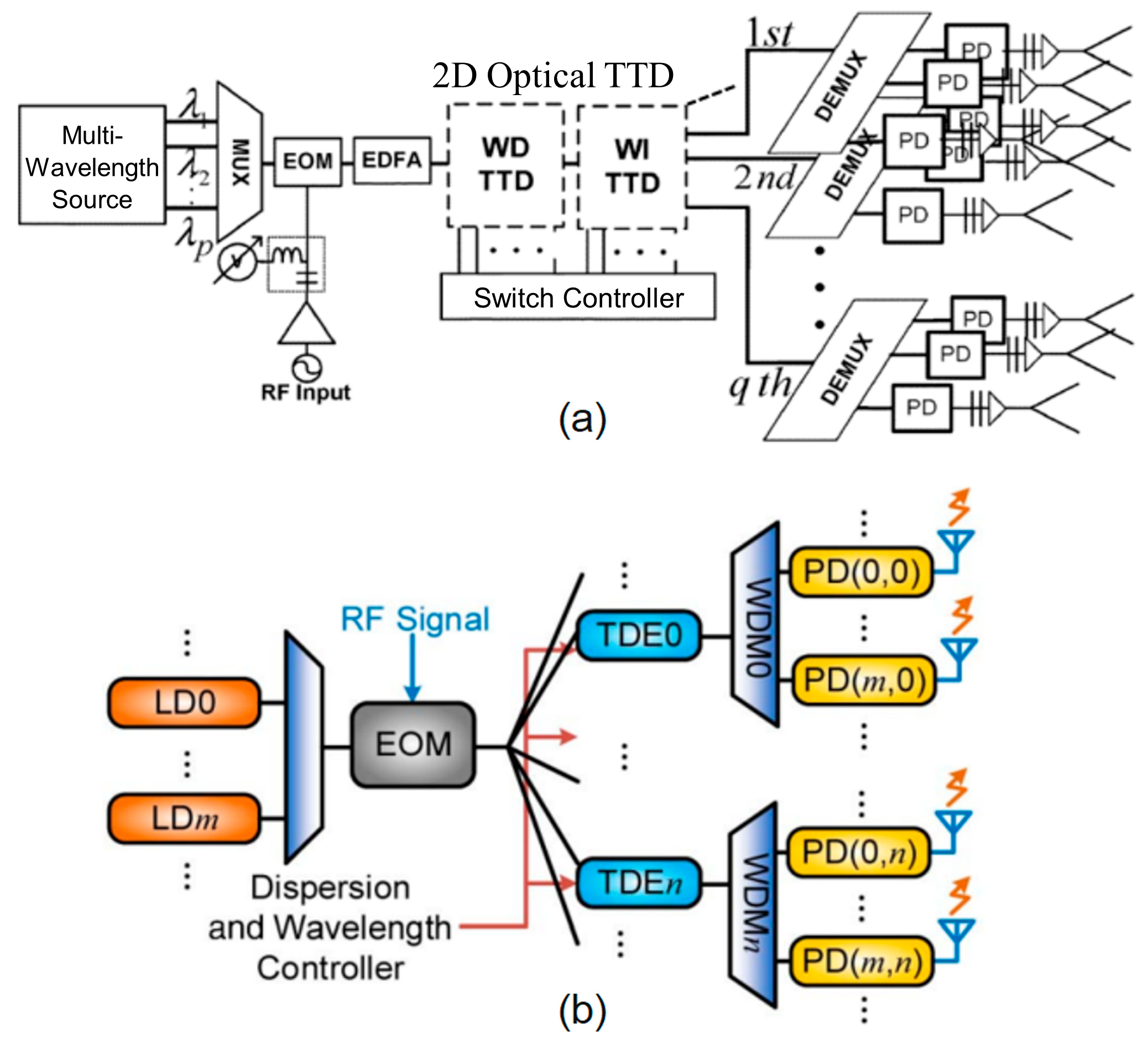
3.5. Time Delay Selection Architectures

The time delay selection architecture is a significant type of OBFNs employing TTD and has squint-free behavior. According to the optical devices exploited for time delay selection, these architectures predominantly include three subclasses as plotted in Figure 13a–c: (1) the architecture with optical switches; (2) the architecture with a wavelength de-multiplexer; (3) the architecture with space light modulators (SLMs). The first architecture uses an optical switch to select the delay lines of various lengths, which is widely studied and several prototypes of small-scale integration have been manufactured [50,73,74,75,76,77]. The optical switch can take advantage of the thermo-optic effect and electro-optic effect, which have a tuning speed of a microsecond scale and nanosecond scale, respectively. Thus, beam sweeping speed can be engineered according to the various requirements of wireless systems. The second architecture (Figure 13b) adopts the wavelength de-multiplexer (DE-MUX) to select different delay lines according to the laser wavelengths; namely, the time delay of each channel in the architecture is determined by the laser wavelength [32,33,78,79]. Once the time delay is selected, the optical signals under different wavelengths are connected to the same PD by a multiplexer (MUX). This architecture can realize nanosecond-scale beam sweeping, resulting from the fast tunable laser which has a switching time of ~1 nanosecond [80]. The third architecture (Figure 13c) selects the time delays of SLMs and polarization beam splitters (PBSs) [18,43,44,81]. Owing to the fact that free-space devices are extensively applied, this architecture has a large size and weight, causing high difficulty for integration. Moreover, the number of antenna elements and structure of 2D planar PAAs should be identical to the pixel number and shape of SLM, which limits the upgrade of the architecture. Nevertheless, the SLMs are commercially available and have small optical loss [82,83], making it easy for this architecture to meet the demand of 2D PAAs with massive antenna elements. One solution to match the pixel number and shape of a SLM with 2D planar PAAs is to utilize a flexible SLM module which can change the pixel number and shape of the SLM [81].
As mentioned earlier, the time delay selection architecture with the wavelength de-multiplexer can tune the time delay by changing the laser wavelength. This architecture adopts multiple optical delay lines for high-resolution beam sweeping. However, these delay lines are used for one antenna, leading to the fact that a massive PAA will utilize a large number of delay lines and increasing the complexity of the system. One approach to simplify the architecture is to allocate one laser wavelength for an antenna, changing the time delay of each antenna using other delay-tuning methods [84,85]. Figure 14 shows one implementation of such an approach with dispersion components, namely linearly chirped fiber Bragg grating (LCFBG) [84]. It is similar to the fiber dispersion architecture in that the time delay difference between adjacent optical channels of the architecture is given by Equation (14) [85], where β is the dispersion coefficient of the LCFBG. This implementation architecture tunes the time delay differences of antennas by changing the wavelength spacing between the adjacent optical channels, thanks to the strain-induced period variation of the fiber Bragg grating with different periods. As a result, the time delay difference, Δτg1, between adjacent channels changes with the variation in λ2λ1. The architecture is based on fibers and fiber components, which have a relatively large size and weight. To realize small-scale integration, integrated de-multiplexers have been applied to simplify the time delay selection architectures with a wavelength multiplexer [32,33]. Furthermore, when using one AWG as a de-multiplexer and the multiplexer simultaneously, the architecture has the potential for more compact integration than does its counterpart with two AWGs [49,78,79].
Δτg1 = β(λ2λ1)
As addressed earlier, 2D optical beamforming is required for 2D planar PAAs. Among the OBFNs with time delay selection architectures, 2D optical beamforming has been achieved by the architectures combined wavelength multiplexers and optical switches or dispersion components. As plotted in Figure 15a, a 2D time delay selection architecture implements wavelength-dependent (WD) TTD and wavelength-independent (WI) TTD to realize horizontal beamforming and vertical beamforming, respectively [48,86]. The WD-TTD adopts fiber Bragg gratings (FBGs) to control time delays for different wavelengths, which is induced by the reflection of the FBGs with various periods, while the WI-TTD uses optical switches to set progressive delays for antenna elements in different rows. It is obvious that a large number of optical switches is demanded in this architecture. For an l-bit × n-bit beamforming system to support a 2D p × q PAA, a total number of l + n × q optical switches is needed. Alternatively, a 2D OBFN architecture with wavelength multiplexers and chirped FBGs (CFBGs), as shown in Figure 15b [87], can be used to reduce the components needed. Owing to the multi-wavelength operation capability of tunable CFBGs, this architecture can tune time delays for antenna elements in one row of PAAs by changing the dispersion of the corresponding CFBG. Meanwhile, the time delay difference between adjacent rows of PAAs is controlled by the center wavelength of the CFBG [88]. Note that, for a similar l-bit × n-bit beamforming system to support a 2D p × q PAA, a total number of p CFBGs is needed in this 2D OBFN architecture in case the tunable CFBG has an l-bit tuning ability. For the small-scale integration of this architecture, the CFBG can be substituted by integrated chirped Bragg grating or chirped sub-wavelength grating [89,90], while the de-multiplexer can be replaced by integrated AWG.

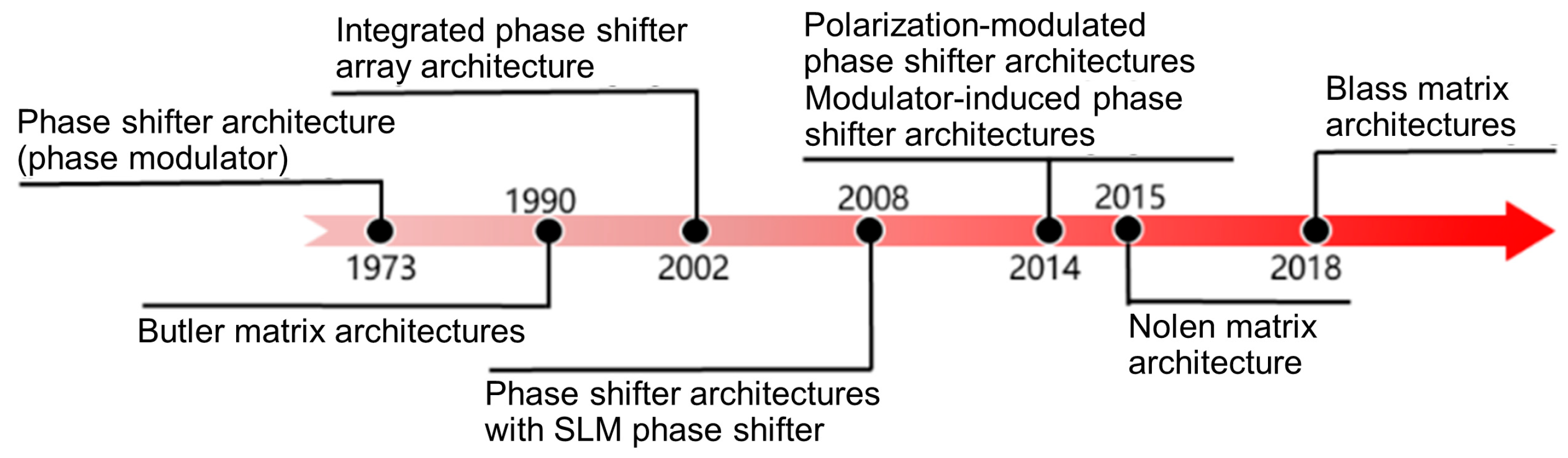
4. OBFNs with Phase Shifter Architectures

The phase shifter architectures are built by an array of optical phase shifters which tune the phases of RF signals. Commonly, the main advantage of this kind of architecture is that the phases of RF signals are equal to phase differences between two optical carriers owing to coherent beating at PDs, as expressed by Equation (9). In other words, the phase shifts of RF signals produced by phase shifter architectures are same as the phase shifts in the optical domain. Phase shifter architectures predominantly include four subclasses: polarization-modulated phase shifter architectures, modulator-induced phase shifter architectures, integrated phase shifter array architectures, matrix architectures (Butler matrix, Blass matrix and Nolen matrix), as shown in Figure 16 [16,22,91,92,93,94,95,96].

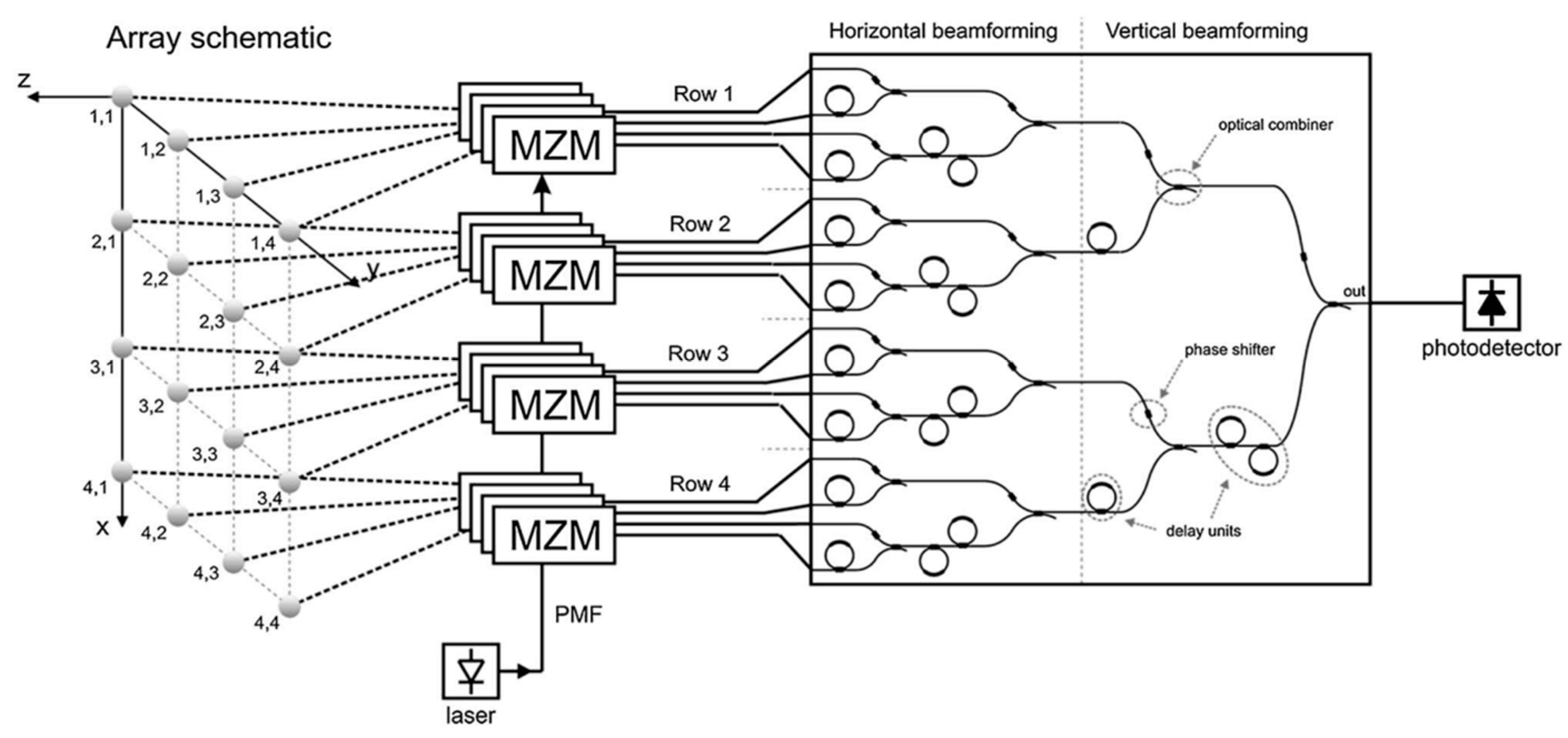
4.1. Polarization-Modulated Phase Shifter Architectures

One phase shifter architecture for the OBFN receiver is presented in Figure 17a, which is a polarization-modulated phase shifter architecture that is composed of a laser diode (LD), a polarization division-multiplexing MZM, a PBS, an optical band-pass filter (OBPF), a 1 × N splitter, N polarization controllers (PCs), N polarizers, and N PDs [97]. Via carrier-suppressed double-sideband modulation at the MZM, sidebands corresponding to the RF signal and local oscillator (LO) signal with orthogonal polarization directions are produced, separately. Then, the upper sidebands of the RF signal and LO signal, extracted by the OBPF, beats at the PD and down-converts into an intermediate frequency (IF) signal in this OBFN receiver architecture. The phase of each IF signal is controlled by the corresponding PC which adjusts the light polarization direction and further tunes the phase difference produced at the polarizer [98]. A similar architecture is presented in Figure 17b, in which the laser light is oriented at an angle of 45° originally and is modulated by a polarization modulator [93]. The functions of the tunable PC, polarizer and OBPF are same as those applied in the architecture before. The phase of the RF signal at one antenna can be given by Equation (15) [25], where ϕi is the phase of one antenna in the PAAs, and αi is the polarization angle between one principal axis of the PolM and the polarization direction aligned by a PC. The phase induced by the phase shifter can vary in a range between 0 and 2π, if αi changes from 0 to π. These architectures both have a key advantage in that the amplitude of the RF signal in each antenna remains unchanged when tuning the phase, since the PC, PBS and polarizer will not influence the magnitude of a circularly polarized optical signal [93]. However, the tuning speed of the PC may be too low to meet the demand of beam sweeping for PAAs. One solution to improve the tuning speed is to use the other PolM to change the phase through the electric control of its DC voltage [99].
ϕ i = π 2 + 2 α i

4.2. Modulator-Induced Phase Shifter Architectures

For optical beamforming, realizing the functions of modulation and the phase shift by the same modulator may largely reduce system complexity, especially for OBFN receivers. OBFNs with this kind of modulator can be called modulator-induced phase shifter architectures. A phase modulator is one kind of such modulators that can be adopted to tune the phase difference of two coherent optical carriers [94]. The phase modulator, manufactured by LiNbO3, has two different electro-optic coefficients for the TE mode and TM mode; namely, the former is one-third of the latter, inducing a phase difference (Δϕi) between the TM mode and TE mode in one channel as (2πVi)/(3Vπ), where Vi is the applied voltage in this channel, and Vπ is the half-wave voltage of the phase modulator [94]. Thus, the phase of the RF signal at each antenna is induced by a phase difference of two coherent optical carriers in the orthogonal polarization direction. The phase difference of adjacent channels in an antenna array can be given by Equation (16), where ΔV is the difference of the applied voltages on the adjacent phase modulators. Additionally, modulation and the phase shift can be realized by a dual-drive MZM, as plotted in Figure 18 [100]. The phase shift in a channel can be induced by the bias voltage of the modulator [101]. The phase difference between adjacent channels can be expressed by Equation (17), where ΔVDC is the difference of bias voltages added on the dual-drive MZMs in adjacent channels. In addition, DMZM is also modulated by the LO signal which has a small frequency difference from the RF signal and down-converts the RF signals into IF signals at the PD. With these phase shifter array architectures, a simplified OBFN without or with less discrete phase shifters can be built for PAAs operating with a given bandwidth. Although fibers are used to connect discrete components, this OBFN architecture has the advantage of immunity to the influence of the environment, due to the fact that the two coherent optical signals employed pass through the same path.
Δϕ = (2πΔV)/(3Vπ)
Δϕ = (πΔVDC)/(3Vπ)

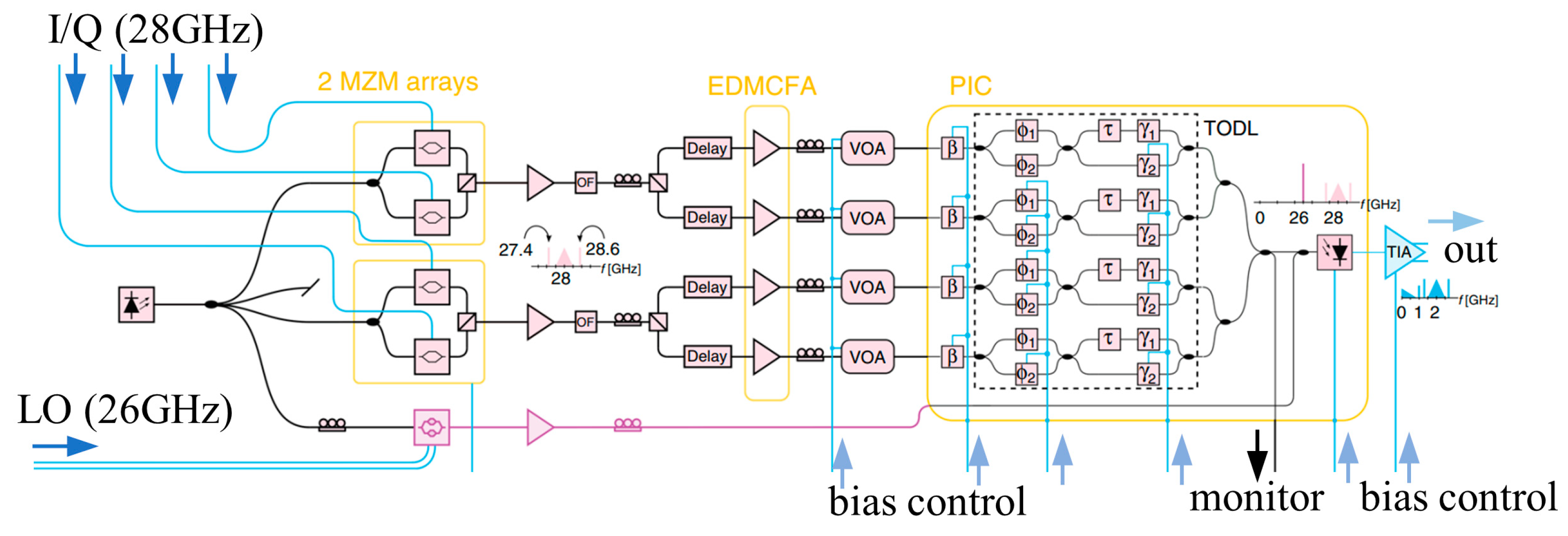
4.3. Integrated Phase Shifter Array Architectures

To miniaturize the OBFNs, multiple phase shifter arrays integrated on one substrate can be employed for phase shifter architectures, owing to the fact that the optical phase shifter has a small footprint for a phase shift in the optical domain. As depicted in Figure 19a, four phase shifters on a silica platform are manufactured for 1 × 4 OBFN [22]. This architecture mainly consists of two lasers, an integrated phase shifter array and four optic/millimeter-wave converters (OMC), namely optic-electric converters. The integrated phase shifter array occupies an area of 2 × 30 mm2. Two lasers are coupled to high modulation sidebands of a master laser (LDM) and have a frequency spacing of 60.8 GHz (19 × 3.2 GHz). Therefore, except for the phase shift, the frequency up-conversion is also realized in the optical domain, which may enhance the value of the OBFNs applied in PAAs. One disadvantage of this architecture is the slow tuning speed of phase shifters using a thermo-optic effect, which is typically tens of or hundreds of microseconds. This issue can be solved by integrating electro-optic phase shifters with a much higher tuning speed. Figure 19b shows the implementation of a phase shifter array architecture using the electro-optic effect, composed of a continuous work (CW) laser, an electro-optic modulator (EOM) with the ability of single-sideband (SSB) modulation, and four beamforming network elements (BFN-E) fabricated on a silicon platform [28,102]. The BFN-E includes an optical filter, an electro-optic phase shifter, and a BPD, which occupies an area of ~4.5 mm2. The optical filter consists of a MRR and MZI structure and separates the optical carrier and the sideband. The electro-optic phase shifter has a tuning speed of 5 ns, which is at least three orders of magnitude faster than that of the thermo-optic phase shifter. Therefore, the integrated phase shifter array architectures is promising for realizing small-scale OBFNs with a beam sweeping speed as fast as hundreds of megahertz. Note that, the loss of the electro-optic phase shifter is larger than that of the thermo-optic phase shifter due to the carrier injection in the waveguide region.

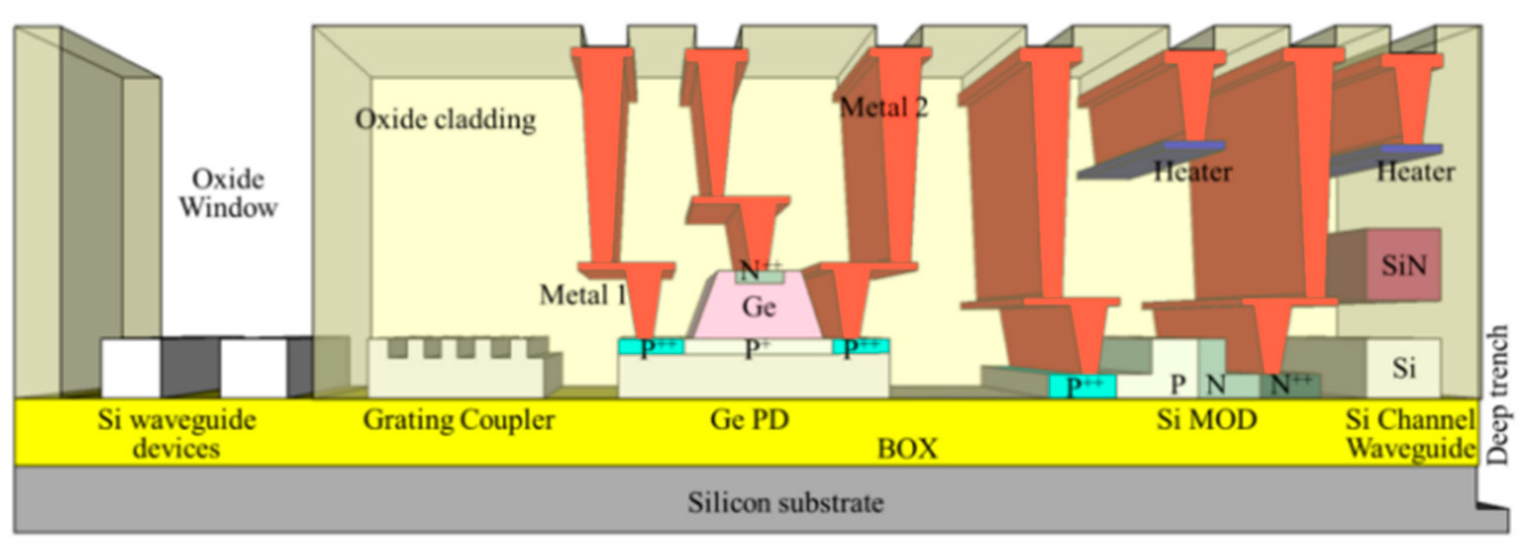
4.4. Matrix Architectures

Matrix architectures, including the Butler matrix, Blass matrix and Nolen matrix are popularly adopted in electric beamforming networks [103,104,105,106]. A distinguished advantage of these architectures is that multi-beam beamforming can be straightforwardly realized when injecting signals into different input ports, in addition to the fact that these architectures have compact structures. There are few works that have adopted these architectures in OBFNs [29,91,95,96,107,108,109,110], in which the optical Butler matrix architecture has the superiorities of footprint and optical loss. Figure 20a shows a 4 × 4 optical Butler matrix which consists of four 3 dB couplers, two phase shifters and a waveguide crossing [111], which is similar to the electrical counterpart. With this structure, each optical signal from one of the input ports will be split into four output ports with a linear phase relationship and an even power. For example, the phases of four optical outputs, when launching from the first input port (In1), are φ1, π/4 + φ1, π/2 + φ1, and 3π/4 + φ1, separately. Using the similar Butler matrix, several implementations for OBFN transmitters and receivers were established [91,107,108,109,110]. For example, a Butler matrix architecture for an OBFN receiver has been demonstrated with an 8 × 8 Butler matrix fabricated on a lithium niobate (LiNbO3) platform with a footprint of ~32 mm × 0.9 mm [91]. Employing this Butler matrix in an OBFN receiver has advantages over using other OBFN receivers since each output of the matrix can combine a high-power LO for increasing the receiving power of the system.
The typical Butler matrix shown above cannot tune the amplitude of the output ports, in order to control the side lobe and grating lobe of the beam pattern formed by the PAA. This issue can be solved by the Blass matrix and Nolen matrix, although these architectures have a larger footprint than that of the Butler matrix. Figure 20b presents a 4 × 4 Blass matrix, in which a tunable coupler together with a phase shifter is served as one node [29]. The phase and amplitude of lights at four outputs can be tuned simultaneously, and each output has the ability to export four optical signals from the four inputs. Based on this principle, an M × N Blass matrix is designed for feeding an N-element PAA [96]. This architecture adopts the self-heterodyne detection technique to produce RF signals. The main operation is as follows. M parts of the optical carrier are modulated by M independent RF signals; then, the upper sidebands are selected by the optical sideband filter and tuned by the M × N Blass matrix, and are coupled with the optical carrier at the couplers and mixed back to the RF signals at PDs. Finally, RF signals are fed to N antennas. In this architecture, M × N phase shifters and tunable couplers are utilized, which occupy a relatively large footprint and need a great number of electric control units. One approach to remediate this issue is to use a Nolen matrix, which reduces the number of nodes to half of that in the Blass matrix. The Nolen matrix has a triangular structure which can also be seen in Figure 20b by ignoring the section below the dashed line. A 144 × 36 Nolen matrix has been reported, and its beamforming pattern has been theoretically investigated [95]. It is worthy to note that the Nolen matrix architecture for OBFN has a footprint that is three orders of magnitude smaller than that of its electric counterpart.
PAAs using phase shifter architectures addressed above are not squint-free, since the phase shift provided by a phase shifter does not depend on the RF frequency, causing a change in the beam angle under different RF frequencies. However, there is a great number of applications with limited bandwidth, while exploiting phase shifters in a TTD architecture can reduce its complexity and cost [18,20,112,113]. For instance, one architecture combined with the phase shifters and TTDs has been proposed in [92,114]. In these two architectures, phase shifters and TTD can realize fine tuning and coarse tuning, separately. This feature is beneficial for scanning the beam in a broad coverage, and achieving a balance between bandwidth and system complexity. Therefore, OBFN architectures with a phase shifter array and TTDs are conducive to PAAs with a limited bandwidth.

5. Scalability and Application Potentials

Up to now, the OBFN architectures implemented have been tested for PAAs with few antenna elements, which may have resulted from the limited optical power of lasers and the large energy dissipation at several components, such as modulators, phase shifters, delay lines and PD. The scalability of OBFNs, including the performances of size, weight, power consumption, loss, bandwidth, multi-beam beamforming and linearity, should be kept in line with the increase in the scale of PAAs. Here, the scalability represents the capability to catch up the development of a wireless communication system with the explosive growth of capacity. In this section, a scalability comparison of different OBFN architectures, scalable techniques and the application potential of OBFNs is discussed.

5.1. Scalability Comparison of Different OBFN Architectures

Table 1 summarizes six performances related to the scalability of OBFN architectures which are elaborated above. The size and weight of OBFNs are intuitive performances corresponding to the number of free-space components and fiber components used in architectures [14]. The power consumptions of OBFNs are mainly induced by lasers, except for the electric and photonic amplifiers [65]. Here, the power consumptions of OBFNs are simply evaluated using the number of lasers applied in these architectures. OBFNs’ loss originates from the insertion loss of components and propagation loss of waveguides. OBFNs’ bandwidth is determined by the mechanisms of time delay and the bandwidth of optical devices. TTD architectures have a wider bandwidth than that of phase shifter array architectures, while MRR and MZI-TTD have a smaller bandwidth than other TTD architectures do since time delays of MRR and MZI-TTD remain constant within a limited frequency range [23,45]. Multi-beam beamforming is a significant ability of OBFNs for massive PAAs which have a narrow beam and should meet the demand of multiusers [9]. The capability of the multi-beam beamforming is assessed via considering the feasibility of producing multiple beams with current architectures. It is shown in Table 1 that, architectures of MRR group delay, MZI delay, photonic crystal, time delay selection with integrated devices, and integrated phase shifter array are of a small size, are light weight and have relatively low power consumption, which are amendable for aerospace applications and pole-mounted base stations. The fiber dispersion delay architectures and time delay selection architectures of SLMs have the advantage of low loss and wide bandwidth. Meanwhile, matrix architectures have the inherently ability of multi-beam beamforming with a relatively small size, weight and power consumption. Therefore, the scalability of these architectures may be evaluated according to the application scenario, while there is not an architecture that can meet the requirements of all applications. For example, the time delay selection architectures of SLMs can easily establish a massive OBFN for massive PAAs in a scenario without considering its size and weight; however, integrated architectures are more appropriate for aerospace antennas and pole-mounted antennas.

5.2. Scalable Techniques for OBFNs

Among the above architectures, MRR group delay architectures, MZI delay architectures, PC delay architectures, integrated time–time delay selection architectures and integrated phase shifter array architectures and matrix architectures are promising for small-scale integration. Nevertheless, these architectures are still of a relatively large size and demand a large number of delay units. For example, a 16 × 1 MRR group delay architecture is adopted to form and steer the beam received by the 4 × 4 2D PAA, which needs 20 MRRs to provide the accurate delays for 16 antennas (Figure 9). It is difficult to scale up this architecture for massive PAAs, since a thermal compensation circuit and a delay control circuit are required for each MRR except for the complexity of delays. One approach is to use the wavelength multiplexing technique as addressed earlier, dramatically decreasing the total number of MRRs from 20 to 8 for the 4 × 4 2D PAA. However, a large amount of lasers, including an integrated laser array, are required for the wavelength multiplexing technique which greatly increases the footprint and cost. One solution is to use microcomb source (Figure 21a [115]) which can largely reduce the size and has the flexibility to meet the demands of different 2D PAAs by changing number of comb lines [56,116]. Furthermore, combining wavelength multiplexing with mode multiplexing, the channel number of integrating OBFNs can be further increased by several times [117], relaxing the requirement of a microcomb source. In addition, photonic field-programmable gate arrays based on microdisk (Figure 21b) and MRR (Figure 21c) can achieve a small footprint, time delay selection, wavelength filtering and reconfiguration simultaneously [118,119]. These structures have potential to be applied in large-scale OBFNs. To sum this up, microcomb sources and programmable structures may provide high scalability for OBFNs used in PAAs with massive antenna elements.
For small-scale integration, a material platform with very low loss is vital for large-scale OBFNs. Currently, photonic integration circuits are predominantly implemented on platforms of silicon (Si), silicon nitride (Si3N4) and indium phosphide (InP). Table 2 lists the propagation losses of these material platforms [120,121,122,123,124,125], in which it is exhibited that the Si3N4 deposited via low-pressure chemical vapor deposition (LPCVD) has the smallest propagation loss, of less than 0.1 dB/cm. The propagation losses of Si and InP fabricated by generic foundries is about 1 dB/cm and 2 dB/cm, respectively, while Si3N4 deposited via plasma-enhanced chemical vapor deposition (PECVD), inductively coupled plasma chemical vapor deposition (ICP-CVD) and reactive sputtering (RS) can also achieve a small loss of ~1 dB/cm. As a result, Si3N4 material, especially the Si3N4 deposited via LPCVD, is promising for the integration of large-scale OBFNs. More recently, a wideband erbium waveguide amplifier was realized based on Si3N4 deposited via LPCVD [126], which may have greatly promoted the photonic integration on the Si3N4 platform. However, the lack of a modulator and PD hinders the full integration of photonic circuits on a Si3N4 platform. One probable approach is to develop a Si-Si3N4 monolithic integration platform as presented in Figure 22, which combines the Si active devices (such as modulator and PD) and Si3N4 passive devices [120,127]. Thus, this Si-Si3N4 photonic platform can capitalize on the advantages of Si3N4 passive devices, Si3N4 waveguide amplifiers and Si active devices.
The heterogeneous integration and monolithic integration of photonic circuits and electrical circuits (electro-photonic systems) are prominent for the compactness, energy efficiency and stability of beamforming systems [11]. The heterogeneous integration of an electro-photonic system can present the advantages of Si3N4 deposition via LPCVD, thanks to the separate fabrication of electric circuits and photonic circuits on different wafers. Meanwhile, the monolithic integration of an electro-photonic system can accelerate the innovation of an electro-photonic system on one substrate [128]. This electro-photonic monolithic integration can be implemented on a silicon-on-insulator (SOI) platform and bulk silicon platform, the latter being more CMOS-compatible [128,129]. To integrate Si3N4 devices on these platforms, Si3N4 material should be fabricated via low-temperature processes such as PECVD, ICP-CVD and RS, instead of LPCVD. Therefore, more efforts should be devoted to manufacturing low-loss photonic circuits and waveguide amplifiers via a low-temperature fabrication process for exploiting the advantages of a Si3N4 platform and the monolithic integration of electro-photonic systems.
In addition, the linearity of OBFNs is also a key factor for scalability, which is mainly determined by the linearity of modulators and PDs [130,131,132]. For microwave photonic systems, such as OBFNs, the linearity of the modulator is critical for the performance of whole system [132]. The linearity of a modulator can be characterized by a spurious free dynamic range (SFDR) defined as the ratio of the maximum RF power which produces third-order intermodulation distortions to noise power. Typically, the SFDR of a silicon-based MZM is smaller than 100 dB∙Hz2/3 at a 1 GHz modulation frequency, exhibiting worse linearity than do LiNbO3 modulators [133]. The linearity of a modulator can be improved using response compensation techniques of MRR and the Kerr effect in a MZM [132,133,134]. Especially, the SFDR of a heterogeneously integrated III–V/Si MZM has been increased to ~117 dB·Hz2/3 at 10 GHz with the assistance of MRR, as shown in Figure 23a. For mmWave wireless communication networks, high-speed and high-power PDs are significant devices as well. The linearity of PDs can be evaluated via a consideration of the maximum output power that approaches the 1 dB compression point [130,135]. One alternative to using high-speed and high-power PDs is to use uni-traveling carrier (UTC) PDs. These PDs have superiorities of low bias voltage, high operation speed and high output power compared to common PDs, since electrons are the majority carriers as shown in Figure 23b [136,137,138]. Currently, UTC-PDs are mainly fabricated on Si/Germanium, InP and InGaAs material platforms [139,140,141]. The maximum output power of Si/Germanium UTC-PDs has reached ~0 dBm at 20 GHz [140,141,142]. Compared to those with a Si/Germanium platform, InP/InGaAs-based UTC-PDs have a wider bandwidth and higher output power, which has resulted in a maximum output power larger than 20 dBm at a low-frequency band of mmWave spectrum such as at 28 GHz, 40 GHz and 48 GHz [130,143,144,145,146]. Therefore, heterogeneous integrations of InP-based UTC-PDs on Si and Si3N4 can be employed [147,148,149], to obtain high-speed and high-power PDs which are comparable to their InP-based counterparts. In summary, it is promising to integrate high-linearity modulators and PDs on Si/ Si3N4 platforms, achieving compact and high-linearity OBFNs.

5.3. Application Potential in Wireless Communication Systems

The application of OBFNs in practical wireless communication system may not be realized in a short time, suffering from the relatively low energy efficiency of electro-optic conversion at the modulator/laser and optic-electric conversion at the PD. Nevertheless, one approach that combines the advantages of analog radio over fiber (A-RoF) and OBFNs has demonstrated application potential in high-frequency wireless communications such as mmWave wireless communication [32,33,34,35,38,150]. This approach implements A-RoF in the mobile fronthaul and OBFNs as beamformers for PAAs. A-RoF technology is a promising alternative for mobile fronthaul, thanks to its high bandwidth efficiency, carrying RF signals directly on the optical signals [7,151]. Recently, A-RoF fronthaul linked with RF signals of high-level modulation formats such as 16 QAM, 32 QAM and 64 QAM have experimentally succeeded and achieved a data rate larger than 1 Gb/s for each beam [152,153,154]. One issue that may hinder the application of the A-RoF with OBFN is its nonlinearity, which results from the laser nonlinear effect, four-wave mixing in optical amplifier and fibers, the nonlinear transfer function of modulators, and the nonlinearity of PDs, as well as the power amplifier [153,155]. OBFNs with high-linearity modulators and high-power PDs provide a solution for this issue. The convergence of an A-RoF fronthaul and OBFN-based PAAs can not only eliminate mixers and digital–analog convertors/analog–digital convertors [32,35], but also remove the lasers and modulators required for OBFNs in antenna sites. This is because OBFNs can be deployed at the central office, which simplifies the antenna units and improves the cost effectiveness and installation flexibility [38,114,152].

6. Conclusions and Outlook

Beamforming and beamsteering through OBFNs provide promising enabling technologies for mmWave wireless communications. In this review, we analyzed typical OBFNs with TTD architectures and phase shifter architectures, introduced their principles and basic features, and conducted a performance comparison of different architectures. Furthermore, several technologies that can scale-up OBFNs were recommended, which include wavelength multiplexing using a microcomb source, MRR/microdisk-based photonic field-programmable gate arrays, the use of low-loss material platforms such as Si3N4, and the heterogeneous and monolithic integration of electro-photonic systems. In addition, integrated devices such as high-linearity modulators and UTC-PDs on Si/Si3N4 platforms are also key components in OBFNs for meeting the demands of mmWave PAAs with massive antenna elements and high excitation power. These two research topics may receive much more concern in the future. For practical applications, the convergence of an OBFN-based PAA and A-RoF is a competitive candidate technology for mmWave wireless communications.

Author Contributions

Conceptualization, F.D.; investigation, F.D., Y.G., Z.G. and Y.Y.; writing—original draft preparation, F.D.; writing—review and editing, F.D., Y.Y., Y.W. and T.C.; funding acquisition, T.C. All authors have read and agreed to the published version of the manuscript.

Funding

This work was supported by Huawei Technologies Co., Ltd.

Data Availability Statement

No new data were created or analyzed in this study. Data sharing is not applicable to this article.

Acknowledgments

The authors would like to thank Xiongbin Yu and Zhipeng Luo from the Huawei Technologies Co., Ltd., for their help with academic writing of this paper.

Conflicts of Interest

The authors declare no conflict of interest.

References

  1. Li, X.; Yu, J.; Chang, G.-K. Photonics-Assisted Technologies for Extreme Broadband 5G Wireless Communications. J. Light. Technol. 2019, 37, 2851–2865. [Google Scholar] [CrossRef]
  2. Chen, Y.W.; Zhang, R.; Hsu, C.W.; Chang, G.K. Key Enabling Technologies for the Post-5G Era: Fully Adaptive, All-Spectra Coordinated Radio Access Network with Function Decoupling. IEEE Commun. Mag. 2020, 58, 60–66. [Google Scholar] [CrossRef]
  3. Tataria, H.; Shafi, M.; Molisch, A.F.; Dohler, M.; Sjöland, H.; Tufvesson, F. 6G Wireless Systems: Vision, Requirements, Challenges, Insights, and Opportunities. Proc. IEEE 2021, 109, 1166–1199. [Google Scholar] [CrossRef]
  4. Hong, W.; Jiang, Z.H.; Yu, C.; Hou, D.; Wang, H.; Guo, C.; Hu, Y.; Kuai, L.; Yu, Y.; Jiang, Z.; et al. The Role of Millimeter-Wave Technologies in 5G/6G Wireless Communications. IEEE J. Microw. 2021, 1, 101–122. [Google Scholar] [CrossRef]
  5. Rappaport, T.S.; Sun, S.; Mayzus, R.; Zhao, H.; Azar, Y.; Wang, K.; Wong, G.N.; Schulz, J.K.; Samimi, M.; Gutierrez, F. Millimeter Wave Mobile Communications for 5G Cellular: It Will Work! IEEE Access 2013, 1, 335–349. [Google Scholar] [CrossRef]
  6. Rappaport, T.S.; Xing, Y.; Kanhere, O.; Ju, S.; Madanayake, A.; Mandal, S.; Alkhateeb, A.; Trichopoulos, G.C. Wireless Communications and Applications Above 100 GHz: Opportunities and Challenges for 6G and beyond. IEEE Access 2019, 7, 78729–78757. [Google Scholar] [CrossRef]
  7. Lim, C.; Tian, Y.; Ranaweera, C.; Nirmalathas, T.A.; Wong, E.; Lee, K.L. Evolution of Radio-Over-Fiber Technology. J. Light. Technol. 2019, 37, 1647–1656. [Google Scholar] [CrossRef]
  8. Paul, B.; Sertel, K.; Nahar, N.K. Photonic Beamforming for 5G and Beyond: A Review of True Time Delay Devices Enabling Ultra-Wideband Beamforming for mmWave Communications. IEEE Access 2022, 10, 75513–75526. [Google Scholar] [CrossRef]
  9. Hong, W.; Jiang, Z.H.; Yu, C.; Zhou, J.; Chen, P.; Yu, Z.; Zhang, H.; Yang, B.; Pang, X.; Jiang, M.; et al. Multibeam Antenna Technologies for 5G Wireless Communications. IEEE Trans. Antennas Propag. 2017, 65, 6231–6249. [Google Scholar] [CrossRef]
  10. Robert, M. Phased Array Antenna Handbook, 3rd ed.; Artech House: Norwood, MA, USA, 2017; p. 1. [Google Scholar]
  11. Cao, Z.; Ma, Q.; Smolders, A.B.; Jiao, Y.; Wale, M.J.; Oh, C.W.; Wu, H.; Koonen, A.M.J. Advanced Integration Techniques on Broadband Millimeter-Wave Beam Steering for 5G Wireless Networks and Beyond. IEEE J. Quantum Electron. 2016, 52, 0600620. [Google Scholar] [CrossRef]
  12. Aldaya, I.; Campuzano, G.; Castañón, G.; Aragón-Zavala, A. A Tutorial on Optical Feeding of Millimeter-Wave Phased Array Antennas for Communication Applications. Int. J. Antennas Propag. 2015, 2015, 264812. [Google Scholar] [CrossRef] [Green Version]
  13. Pan, S.; Ye, X.; Zhang, Y.; Zhang, F. Microwave Photonic Array Radars. IEEE J. Microw. 2021, 1, 176–190. [Google Scholar] [CrossRef]
  14. Anzalchi, J.; Perrott, R.; Latunde-Dada, K.; Oldenbeuving, R.; Roeloffzen, C.G.; Van Dijk, P.W.; Hoekman, M.; Leeuwis, H.; Leinse, A. Optical beamforming based on microwave photonic signal processing. In Proceedings of the International Conference on Space Optics (ICSO), Biarritz, France, 18–21 October 2016. [Google Scholar]
  15. Pan, S.; Zhang, Y. Microwave Photonic Radars. J. Light. Technol. 2020, 38, 5450–5484. [Google Scholar] [CrossRef]
  16. Cumming, R.C.; Matt, L.; Wright, M.L. Optically Operated Microwave Phased-Array Antenna System. U.S. Patent 3,878,520, 15 April 1975. [Google Scholar]
  17. Levine, A.M. Fiber Optic Phased Array Antenna System for RF Transmission. U.S. Patent 4,028,702, 7 June 1977. [Google Scholar]
  18. Goutzoulis, A.; Davies, K.; Zomp, J.; Hrycak, P.; Johnson, A. Development and field demonstration of a hardware-compressive fiber-optic true-time-delay steering system for phased-array antennas. Appl. Opt. 1994, 33, 8173–8185. [Google Scholar] [CrossRef]
  19. Dolfi, D.; Michel-Gabriel, F.; Bann, S.; Huignard, J.P. Two-dimensional optical architecture for time-delay beam forming in a phased-array antenna. Opt. Lett. 1991, 16, 255–257. [Google Scholar] [CrossRef] [PubMed]
  20. Frigyes, I.; Seeds, A.J. Optically generated true-time delay in phased-array antennas. IEEE Trans. Microw. Theory Tech. 1995, 43, 2378–2386. [Google Scholar] [CrossRef]
  21. Capmany, J.; Novak, D. Microwave photonics combines two worlds. Nat. Photonics 2007, 1, 319–330. [Google Scholar] [CrossRef]
  22. Grosskopf, G.; Eggemann, R.; Zinal, S.; Kuhlow, B.; Przyrembel, G.; Rohde, D.; Kortke, A.; Ehlers, H. Photonic 60-GHz maximum directivity beam former for smart antennas in mobile broad-band communications. IEEE Photonics Technol. Lett. 2002, 14, 1169–1171. [Google Scholar] [CrossRef]
  23. Meijerink, A.; Roeloffzen, C.G.H.; Meijerink, R.; Zhuang, L.; Marpaung, D.A.I.; Bentum, M.J.; Burla, M.; Verpoorte, J.; Jorna, P.; Hulzinga, A.; et al. Novel Ring Resonator-Based Integrated Photonic Beamformer for Broadband Phased Array Receive Antennas—Part I: Design and Performance Analysis. J. Light. Technol. 2010, 28, 3–18. [Google Scholar] [CrossRef] [Green Version]
  24. Zhuang, L.; Roeloffzen, C.G.H.; Meijerink, A.; Burla, M.; Marpaung, D.A.I.; Leinse, A.; Hoekman, M.; Heideman, R.G.; Etten, W.v. Novel Ring Resonator-Based Integrated Photonic Beamformer for Broadband Phased Array Receive Antennas—Part II: Experimental Prototype. J. Light. Technol. 2010, 28, 19–31. [Google Scholar] [CrossRef] [Green Version]
  25. Pan, S.; Zhang, Y. Tunable and wideband microwave photonic phase shifter based on a single-sideband polarization modulator and a polarizer. Opt. Lett. 2012, 37, 4483–4485. [Google Scholar] [CrossRef] [PubMed] [Green Version]
  26. Liu, Y.; Wichman, A.R.; Isaac, B.; Kalkavage, J.; Adles, E.J.; Clark, T.R.; Klamkin, J. Ultra-Low-Loss Silicon Nitride Optical Beamforming Network for Wideband Wireless Applications. IEEE J. Sel. Top. Quantum Electron. 2018, 24, 8300410. [Google Scholar] [CrossRef]
  27. Duarte, V.C.; Prata, J.G.; Ribeiro, C.F.; Nogueira, R.N.; Winzer, G.; Zimmermann, L.; Walker, R.; Clements, S.; Filipowicz, M.; Napierała, M.; et al. Modular coherent photonic-aided payload receiver for communications satellites. Nat. Commun. 2019, 10, 1984. [Google Scholar] [CrossRef] [PubMed] [Green Version]
  28. Serafino, G.; Porzi, C.; Hussain, B.; Scotti, F.; Falconi, F.; Chiesa, M.; Toccafondo, V.; Bogoni, A.; Ghelfi, P. High-Performance Beamforming Network Based on Si-Photonics Phase Shifters for Wideband Communications and Radar Applications. IEEE J. Sel. Top. Quantum Electron. 2020, 26, 6101011. [Google Scholar] [CrossRef]
  29. Muñoz, R.; Rommel, S.; Dijk, P.v.; Brenes, J.; Grivas, E.; Manso, C.; Roeloffzen, C.; Vilalta, R.; Fabrega, J.M.; Landi, G.; et al. Experimental Demonstration of Dynamic Optical Beamforming for Beyond 5G Spatially Multiplexed Fronthaul Networks. IEEE J. Sel. Top. Quantum Electron. 2021, 27, 8600216. [Google Scholar] [CrossRef]
  30. Santacruz, J.P.; Rommel, S.; Roeloffzen, C.G.H.; Timens, R.B.; Dijk, P.W.L.; Jurado-Navas, A.; Monroy, I.T. Incoherent Optical Beamformer for ARoF Fronthaul in Mm-Wave 5G/6G Networks. J. Light. Technol. 2022, 41, 1325–1334. [Google Scholar] [CrossRef]
  31. Sun, H.; Lu, L.; Liu, Y.; Ni, Z.; Chen, J.; Zhou, L. Broadband 1×8 Optical Beamforming Network Based on Anti-resonant Microring Delay Lines. J. Light. Technol. 2022, 40, 6919–6928. [Google Scholar] [CrossRef]
  32. Cao, Z.; Zhao, X.; Soares, F.M.; Tessema, N.; Koonen, A.M.J. 38-GHz Millimeter Wave Beam Steered Fiber Wireless Systems for 5G Indoor Coverage: Architectures, Devices, and Links. IEEE J. Quantum Electron. 2017, 53, 8000109. [Google Scholar] [CrossRef]
  33. Zhang, X.; Zhao, M.; Jiao, Y.; Cao, Z.; Koonen, A.M.J. Integrated Wavelength-Tuned Optical mm-Wave Beamformer with Doubled Delay Resolution. J. Light. Technol. 2020, 38, 2353–2359. [Google Scholar] [CrossRef]
  34. Moerman, A.; Kerrebrouck, J.V.; Caytan, O.; Paula, I.L.d.; Bogaert, L.; Torfs, G.; Demeester, P.; Rogier, H.; Lemey, S. Beyond 5G without Obstacles: mmWave-over-Fiber Distributed Antenna Systems. IEEE Commun. Mag. 2022, 60, 27–33. [Google Scholar] [CrossRef]
  35. Paula, I.L.d.; Bogaert, L.; Caytan, O.; Kerrebrouck, J.V.; Moerman, A.; Muneeb, M.; Brande, Q.V.d.; Torfs, G.; Bauwelinck, J.; Rogier, H.; et al. Air-Filled SIW Remote Antenna Unit with True Time Delay Optical Beamforming for mmWave-Over-Fiber Systems. J. Light. Technol. 2022, 40, 6961–6975. [Google Scholar] [CrossRef]
  36. Lu, F.; Xu, M.; Shen, S.; Alfadhli, Y.M.; Cho, H.J.; Chang, G.K. Demonstration of Inter-Dimensional Adaptive Diversity Combining and Repetition Coding in Converged MMW/FSO Links for 5G and beyond Mobile Fronthaul. In Proceedings of the Optical Fiber Communications Conference and Exposition, San Diego, CA, USA, 11 March 2018. [Google Scholar]
  37. Zhang, R.; Lu, F.; Xu, M.; Liu, S.; Peng, P.C.; Shen, S.; He, J.; Cho, H.J.; Zhou, Q.; Yao, S.; et al. An Ultra-Reliable MMW/FSO A-RoF System Based on Coordinated Mapping and Combining Technique for 5G and Beyond Mobile Fronthaul. J. Light. Technol. 2018, 36, 4952–4959. [Google Scholar] [CrossRef]
  38. Morant, M.; Trinidad, A.; Tangdiongga, E.; Koonen, T.; Llorente, R. Experimental Demonstration of mm-Wave 5G NR Photonic Beamforming Based on ORRs and Multicore Fiber. IEEE Trans. Microw. Theory Tech. 2019, 67, 2928–2935. [Google Scholar] [CrossRef]
  39. Rotman, R.; Tur, M.; Yaron, L. True Time Delay in Phased Arrays. Proc. IEEE 2016, 104, 504–518. [Google Scholar] [CrossRef]
  40. John, L.V. Antenna Engineering Handbook, 4th ed.; McGraw-Hill Education: New York, NY, USA, 2007; pp. 3-4–3-13. [Google Scholar]
  41. Zhou, L.; Wang, X.; Lu, L.; Chen, J. I Integrated optical delay lines: A review and perspective nvited. Chin. Opt. Lett. 2018, 16, 101301. [Google Scholar] [CrossRef] [Green Version]
  42. Esman, R.D.; Frankel, M.Y.; Dexter, J.L.; Goldberg, L.; Parent, M.G.; Stilwell, D.; Cooper, D.G. Fiber-optic prism true time-delay antenna feed. IEEE Photonics Technol. Lett. 1993, 5, 1347–1349. [Google Scholar] [CrossRef]
  43. Frankel, M.Y.; Matthews, P.J.; Esman, R.D. Two-dimensional fiber-optic control of a true time-steered array transmitter. IEEE Trans. Microw. Theory Tech. 1996, 44, 2696–2702. [Google Scholar] [CrossRef]
  44. Riza, N.A. Transmit/receive time-delay beam-forming optical architecture for phased-array antennas. Appl. Opt. 1991, 30, 4594–4595. [Google Scholar] [CrossRef]
  45. Duarte, V.C.; Drummond, M.V.; Nogueira, R.N. Photonic True-Time-Delay Beamformer for a Phased Array Antenna Receiver based on Self-Heterodyne Detection. J. Light. Technol. 2016, 34, 5566–5575. [Google Scholar] [CrossRef]
  46. Lin, C.-Y.; Subbaraman, H.; Hosseini, A.; Wang, A.X.; Zhu, L.; Chen, R.T. Silicon nanomembrane based photonic crystal waveguide array for wavelength-tunable true-time-delay lines. Appl. Phys. Lett. 2012, 101, 051101. [Google Scholar] [CrossRef] [Green Version]
  47. Burla, M.; Roeloffzen, C.G.H.; Zhuang, L.; Marpaung, D.; Khan, M.R.; Maat, P.; Dijkstra, K.; Leinse, A.; Hoekman, M.; Heideman, R. System integration and radiation pattern measurements of a phased array antenna employing an integrated photonic beamformer for radio astronomy applications. Appl. Opt. 2012, 51, 789–802. [Google Scholar] [CrossRef] [PubMed]
  48. Jung, B.M.; Shin, J.D.; Kim, B.G. Optical True Time-Delay for Two-Dimensional X-Band Phased Array Antennas. IEEE Photonics Technol. Lett. 2007, 19, 877–879. [Google Scholar] [CrossRef]
  49. Piqueras, M.A.; Grosskopf, G.; Vidal, B.; Herrera, J.; Martinez, J.M.; Sanchis, P.; Polo, V.; Corral, J.L.; Marceaux, A.; Galiere, J.; et al. Optically beamformed beam-switched adaptive antennas for fixed and mobile broad-band wireless access networks. IEEE Trans. Microw. Theory Tech. 2006, 54, 887–899. [Google Scholar] [CrossRef] [Green Version]
  50. Rasras, M.S.; Madsen, C.K.; Cappuzzo, M.A.; Chen, E.; Gomez, L.T.; Laskowski, E.J.; Griffin, A.; Wong-Foy, A.; Gasparyan, A.; Kasper, A.; et al. Integrated resonance-enhanced variable optical delay lines. IEEE Photonics Technol. Lett. 2005, 17, 834–836. [Google Scholar] [CrossRef]
  51. Ye, X.; Zhang, F.; Pan, S. Optical true time delay unit for multi-beamforming. Opt. Express 2015, 23, 10002–10008. [Google Scholar] [CrossRef] [Green Version]
  52. Furuya, K.; Hirasawa, T.; Oishi, M.; Akiba, S.; Hirokawa, J.; Ando, M. 60 GHz-Band Photonic-Integrated Array-Antenna and Module for Radio-over-Fiber-Based Beam Forming. IEICE Trans. Commun. 2017, 100-B, 1717–1725. [Google Scholar] [CrossRef] [Green Version]
  53. Esman, R.D.; Monsma, M.J.; Dexter, J.L.; Cooper, D.G. Microwave true time-delay modulator using fibre-optic dispersion. Electron. Lett. 1992, 28, 1905–1908. [Google Scholar] [CrossRef]
  54. Gustavsson, U.; Frenger, P.; Fager, C.; Eriksson, T.; Zirath, H.; Dielacher, F.; Studer, C.; Pärssinen, A.; Correia, R.; Matos, J.N.; et al. Implementation Challenges and Opportunities in Beyond-5G and 6G Communication. IEEE J. Microw. 2021, 1, 86–100. [Google Scholar] [CrossRef]
  55. Hu, Y.; Zhan, J.; Jiang, Z.H.; Yu, C.; Hong, W. An Orthogonal Hybrid Analog–Digital Multibeam Antenna Array for Millimeter-Wave Massive MIMO Systems. IEEE Trans. Antennas Propag. 2021, 69, 1393–1403. [Google Scholar] [CrossRef]
  56. Zhang, C.; Lei, P.; Liu, R.; He, B.; Chen, Z.; Xie, X.; Hu, W. Large-scale true-time-delay remote beamforming with EO frequency combs and multicore fiber. Opt. Lett. 2021, 46, 3793–3796. [Google Scholar] [CrossRef]
  57. Burla, M.; Khan, M.R.H.; Marpaung, D.A.I.; Roeloffzen, C.G.H.; Maat, P.; Dijkstra, K.; Leinse, A.; Hoekman, M.; Heideman, R. Squint-free beamsteering demonstration using a photonic integrated beamformer based on optical ring resonators. In Proceedings of the IEEE International Topical Meeting on Microwave Photonics, Montreal, QC, Canada, 5–9 October 2010. [Google Scholar]
  58. Liu, Y.; Wichman, A.; Isaac, B.; Kalkavage, J.; Adles, E.J.; Clark, T.R.; Klamkin, J. Tuning Optimization of Ring Resonator Delays for Integrated Optical Beam Forming Networks. J. Light. Technol. 2017, 35, 4954–4960. [Google Scholar] [CrossRef]
  59. Abbas, G.; Chan, V.; Ting, Y. A dual-detector optical heterodyne receiver for local oscillator noise suppression. J. Light. Technol. 1985, 3, 1110–1122. [Google Scholar] [CrossRef] [Green Version]
  60. Meijerink, A.; Roeloffzen, C.G.H.; Zhuang, L.; Marpaung, D.A.I.; Heideman, R.G.; Borreman, A.; Etten, W.v. Phased Array Antenna Steering Using a Ring Resonator-Based Optical Beam Forming Network. In Proceedings of the Symposium on Communications and Vehicular Technology, Liege, Belgium, 23 November 2006. [Google Scholar]
  61. Zhuang, L.; Roeloffzen, C.G.H.; Heideman, R.G.; Borreman, A.; Meijerink, A.; Etten, W.v. Single-Chip Ring Resonator-Based 1×8 Optical Beam Forming Network in CMOS-Compatible Waveguide Technology. IEEE Photonics Technol. Lett. 2007, 19, 1130–1132. [Google Scholar] [CrossRef]
  62. Schippers, H.; Verpoorte, J.; Jorna, P.; Hulzinga, A.; Zhuang, L.; Meijerink, A.; Roeloffzen, C.G.H.; Marpaung, D.A.I.; Etten, W.v.; Heideman, R.G.; et al. Broadband optical beam forming for airborne phased array antenna. In Proceedings of the IEEE Aerospace conference, Big Sky, MT, USA, 7–14 March 2009. [Google Scholar]
  63. Burla, M.; Khan, R.; Zhuang, L.; Roeloffzen, C. Multiwavelength optical beam forming network with ring resonator-based binary-tree architecture for broadband phased array antenna systems. In Proceedings of the 13th Annual Symposium of the IEEE/LEOS Benelux Chapter, Enschede, The Netherlands, 27–28 November 2008. [Google Scholar]
  64. Burla, M.; Marpaung, D.A.I.; Zhuang, L.; Khan, M.R.; Leinse, A.; Beeker, W.; Hoekman, M.; Heideman, R.G.; Roeloffzen, C.G.H. Multiwavelength-Integrated Optical Beamformer Based on Wavelength Division Multiplexing for 2-D Phased Array Antennas. J. Light. Technol. 2014, 32, 3509–3520. [Google Scholar] [CrossRef]
  65. Duarte, V.; Prata, J.; Nogueira, R.; Winzer, G.; Zimmermann, L.; Walker, R.; Clements, S.; Filipowicz, M.; Napierala, M.; Nasilowski, T.; et al. Modular and smooth introduction of photonics in high-throughput communication satellites—Perspective of project BEACON. In Proceedings of the International Conference on Space Optics (ICSO), Chania, Greece, 9–12 October 2018. [Google Scholar]
  66. Drummond, M.V.; Monteiro, P.P.; Nogueira, R.N. Photonic True-Time Delay Beamforming Based on Polarization-Domain Interferometers. J. Light. Technol. 2010, 28, 2492–2498. [Google Scholar] [CrossRef]
  67. Baba, T. Slow light in photonic crystals. Nat. Photonics 2008, 2, 465–473. [Google Scholar] [CrossRef]
  68. Yongqiang, J.; Howley, B.; Zhong, S.; Qingjun, Z.; Chen, R.T.; Chen, M.Y.; Brost, G.; Lee, C. Dispersion-enhanced photonic crystal fiber array for a true time-delay structured X-band phased array antenna. IEEE Photonics Technol. Lett. 2005, 17, 187–189. [Google Scholar] [CrossRef]
  69. Ishikura, N.; Hosoi, R.; Hayakawa, R.; Tamanuki, T.; Shinkawa, M.; Baba, T. Photonic crystal tunable slow light device integrated with multi-heaters. Appl. Phys. Lett. 2012, 100, 221110. [Google Scholar] [CrossRef] [Green Version]
  70. Takeuchi, G.; Terada, Y.; Takeuchi, M.; Abe, H.; Ito, H.; Baba, T. Thermally controlled Si photonic crystal slow light waveguide beam steering device. Optics Express 2018, 26, 11529–11537. [Google Scholar] [CrossRef] [Green Version]
  71. Ito, H.; Kusunoki, Y.; Maeda, J.; Akiyama, D.; Kodama, N.; Abe, H.; Tetsuya, R.; Baba, T. Wide beam steering by slow-light waveguide gratings and a prism lens. Optica 2020, 7, 47–52. [Google Scholar] [CrossRef]
  72. Tamanuki, T.; Ito, H.; Baba, T. Thermo-Optic Beam Scanner Employing Silicon Photonic Crystal Slow-Light Waveguides. J. Light. Technol. 2021, 39, 904–911. [Google Scholar] [CrossRef]
  73. Fathpour, S.; Riza, N. Silicon-photonics-based wideband radar beamforming: Basic design. Opt. Eng. 2010, 49, 018201. [Google Scholar] [CrossRef]
  74. Wang, X.; Zhou, L.; Li, R.; Xie, J.; Lu, L.; Wu, K.; Chen, J. Continuously tunable ultra-thin silicon waveguide optical delay line. Optica 2017, 4, 507–515. [Google Scholar] [CrossRef]
  75. Liu, Y.; Isaac, B.; Kalkavage, J.; Adles, E.; Clark, T.; Klamkin, J. 93-GHz Signal Beam Steering with True Time Delayed Integrated Optical Beamforming Network. In Proceedings of the Optical Fiber Communication Conference, San Diego, CA, USA, 3 March 2019. [Google Scholar]
  76. Trinidad, A.M.; Cao, Z.; van Zantvoort, J.H.C.; Tangdiongga, E.; Koonen, A.M.J. Broadband and continuous beamformer based on switched delay lines cascaded by optical ring resonator. In Proceedings of the Optical Fiber Communication Conference, San Diego, CA, USA, 3 March 2019. [Google Scholar]
  77. Zhu, C.; Lu, L.; Shan, W.; Xu, W.; Zhou, G.; Zhou, L.; Chen, J. Silicon integrated microwave photonic beamformer. Optica 2020, 7, 1162–1170. [Google Scholar] [CrossRef]
  78. Yaron, L.; Rotman, R.; Zach, S.; Tur, M. Photonic Beamformer Receiver with Multiple Beam Capabilities. IEEE Photonics Technol. Lett. 2010, 22, 1723–1725. [Google Scholar] [CrossRef]
  79. Tessema, N.; Yan, F.; Cao, Z.; Tangdiongga, E.; Koonen, A.M.J. Compact and tunable AWG-based true-time delays for multi-Gbps radio beamformer. In Proceedings of the European Conference on Optical Communication (ECOC), Valencia, Spain, 27 September 2015. [Google Scholar]
  80. Vidal, B.; Mengual, T.; Martí, J. Fast Optical Beamforming Architectures for Satellite-Based Applications. Adv. Opt. Technol. 2012, 2012, 385409. [Google Scholar] [CrossRef] [Green Version]
  81. Riza, N.A.; Khan, S.A.; Arain, M.A. Flexible beamforming for optically controlled phased array antennas. Opt. Commun. 2003, 227, 301–310. [Google Scholar] [CrossRef]
  82. Beeckman, J.; Neyts, K.; Vanbrabant, P. Liquid-crystal photonic applications. Opt. Eng. 2011, 50, 081202. [Google Scholar] [CrossRef] [Green Version]
  83. Bleha, W.; Lei, L.A. Advances in Liquid Crystal on Silicon (LCOS) spatial light modulator technology. In Proceedings of the SPIE Defense, Security, and Sensing, Baltimore, MA, USA, 4 June 2013. [Google Scholar]
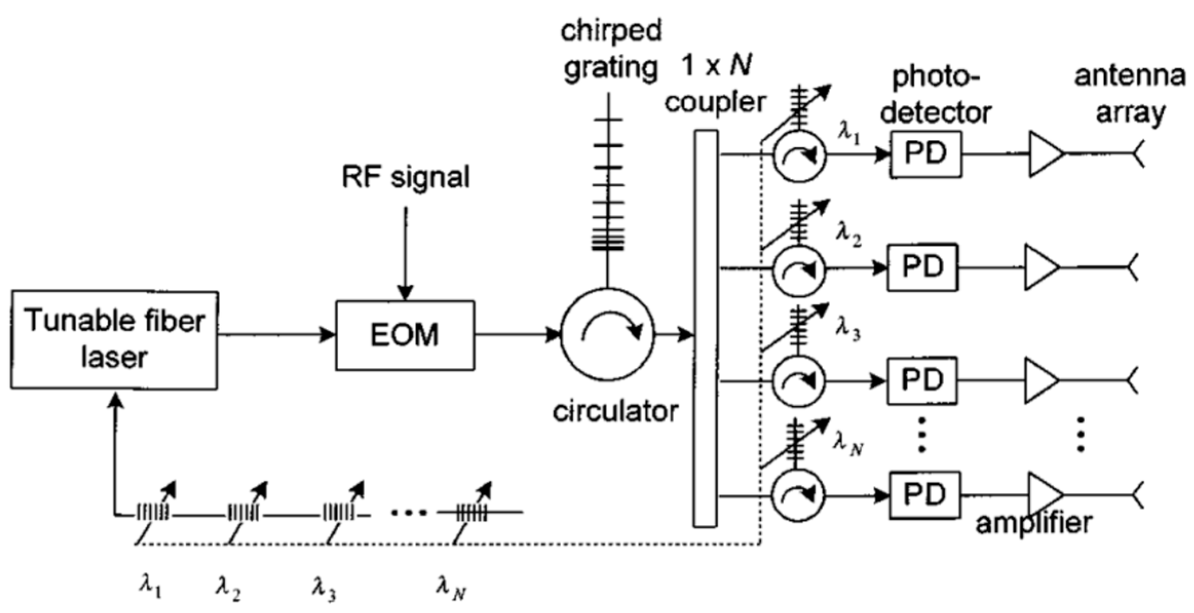
  84. Jianping, Y.; Jianliang, Y.; Yunqi, L. Continuous true-time-delay beamforming employing a multiwavelength tunable fiber laser source. IEEE Photonics Technol. Lett. 2002, 14, 687–689. [Google Scholar] [CrossRef]
  85. Zhang, J.; Yao, J. Photonic True-Time Delay Beamforming Using a Switch-Controlled Wavelength-Dependent Recirculating Loop. J. Light. Technol. 2016, 34, 3923–3929. [Google Scholar] [CrossRef]
  86. Jung, B.M.; Yao, J. A Two-Dimensional Optical True Time-Delay Beamformer Consisting of a Fiber Bragg Grating Prism and Switch-Based Fiber-Optic Delay Lines. IEEE Photonics Technol. Lett. 2009, 21, 627–629. [Google Scholar] [CrossRef]
  87. Ye, X.; Zhang, F.; Pan, S. Compact optical true time delay beamformer for a 2D phased array antenna using tunable dispersive elements. Opt. Lett. 2016, 41, 3956–3959. [Google Scholar] [CrossRef] [Green Version]
  88. Painchaud, Y.; Paquet, C.; Guy, M. Optical Tunable Dispersion Compensators based on Thermally Tuned Fiber Bragg Gratings. Opt. Photon. News 2007, 18, 48–53. [Google Scholar] [CrossRef]
  89. Spasojevic, M.; Chen, L.R. Discretely tunable optical delay lines using serial and step-chirped sidewall Bragg gratings in SOI. Electron. Lett. 2013, 49, 608–610. [Google Scholar] [CrossRef]
  90. Sun, H.; Wang, Y.; Chen, L.R. Integrated Discretely Tunable Optical Delay Line Based on Step-Chirped Subwavelength Grating Waveguide Bragg Gratings. J. Light. Technol. 2020, 38, 5551–5560. [Google Scholar] [CrossRef]
  91. Charczenko, W.; Surette, M.; Matthews, P.; Klotz, H.; Mickelson, A. Integrated optical Butler matrix for beam forming in phased-array antennas. In Proceedings of the Optoelectronic Signal Processing for Phase-Array Antennas II, Los Angeles, CA, USA, 1 June 1990. [Google Scholar]
  92. Jofre, L.; Stoltidou, C.; Blanch, S.; Mengual, T.; Vidal, B.; Marti, J.; McKenzie, I.; Cura, J.M.d. Optically Beamformed Wideband Array Performance. IEEE Trans. Antennas Propag. 2008, 56, 1594–1604. [Google Scholar] [CrossRef] [Green Version]
  93. Zhang, Y.; Wu, H.; Zhu, D.; Pan, S. An optically controlled phased array antenna based on single sideband polarization modulation. Optics Express 2014, 22, 3761–3765. [Google Scholar] [CrossRef]
  94. Shi, S.; Bai, J.; Schneider, G.J.; Zhang, Y.; Nelson, R.; Wilson, J.; Schuetz, C.; Grund, D.W.; Prather, D.W. Conformal Wideband Optically Addressed Transmitting Phased Array with Photonic Receiver. J. Light. Technol. 2014, 32, 3468–3477. [Google Scholar] [CrossRef]
  95. Roeloffzen, C.G.H.; Oldenbeuving, R.M.; Timens, R.B.; van Dijk, P.W.L.; Taddei, C.; Leinse, A.; Hoekman, M.; Heideman, R.G.; Zhuang, L.; Marpaung, D.A.I.; et al. Integrated Optical Beamformers. In Proceedings of the Optical Fiber Communication Conference, Los Angeles, CA, USA, 22 March 2015. [Google Scholar]
  96. Tsokos, C.; Mylonas, E.; Groumas, P.; Katopodis, V.; Gounaridis, L.; Timens, R.B.; Oldenbeuving, R.M.; Roeloffzen, C.G.H.; Avramopoulos, H.; Kouloumentas, C. Analysis of a Multibeam Optical Beamforming Network Based on Blass Matrix Architecture. J. Light. Technol. 2018, 36, 3354–3372. [Google Scholar] [CrossRef]
  97. Gao, Y.; Wen, A.; Tu, Z.; Zhang, W.; Lin, L. Simultaneously photonic frequency downconversion, multichannel phase shifting, and IQ demodulation for wideband microwave signals. Opt. Lett. 2016, 41, 4484–4487. [Google Scholar] [CrossRef]
  98. Gao, Y.; Wen, A.; Liu, L.; Tian, S.; Xiang, S.; Wang, Y. Compensation of the Dispersion-Induced Power Fading in an Analog Photonic Link Based on PM–IM Conversion in a Sagnac Loop. J. Light. Technol. 2015, 33, 2899–2904. [Google Scholar] [CrossRef]
  99. Zhang, W.; Yao, J. Ultrawideband RF Photonic Phase Shifter Using Two Cascaded Polarization Modulators. IEEE Photonics Technol. Lett. 2014, 26, 911–914. [Google Scholar] [CrossRef]
  100. Jiang, T.; Yu, S.; Wu, R.; Wang, D.; Gu, W. Photonic downconversion with tunable wideband phase shift. Opt. Lett. 2016, 41, 2640–2643. [Google Scholar] [CrossRef] [PubMed]
  101. Dubovitsky, S.; Steier, W.H.; Yegnanarayanan, S. Analysis and Improvement of Mach-Zehnder Modulator Linearity Performance for Chirped and Tunable Optical Carriers. J. Light. Technol. 2002, 20, 858. [Google Scholar] [CrossRef]
  102. Porzi, C.; Serafino, G.; Sans, M.; Falconi, F.; Sorianello, V.; Pinna, S.; Mitchell, J.E.; Romagnoli, M.; Bogoni, A.; Ghelfi, P. Photonic Integrated Microwave Phase Shifter up to the mm-Wave Band with Fast Response Time in Silicon-on-Insulator Technology. J. Light. Technol. 2018, 36, 4494–4500. [Google Scholar] [CrossRef] [Green Version]
  103. Lin, T.H.; Hsu, S.K.; Wu, T.L. Bandwidth Enhancement of 4 × 4 Butler Matrix Using Broadband Forward-Wave Directional Coupler and Phase Difference Compensation. IEEE Trans. Microw. Theory Tech. 2013, 61, 4099–4109. [Google Scholar] [CrossRef]
  104. Zhong, L.H.; Ban, Y.L.; Lian, J.W.; Yang, Q.L.; Guo, J.; Yu, Z.F. Miniaturized SIW Multibeam Antenna Array Fed by Dual-Layer 8 × 8 Butler Matrix. IEEE Antennas Wirel. Propag. Lett. 2017, 16, 3018–3021. [Google Scholar] [CrossRef]
  105. Lian, J.W.; Ban, Y.L.; Xiao, C.; Yu, Z.F. Compact Substrate-Integrated 4 × 8 Butler Matrix with Sidelobe Suppression for Millimeter-Wave Multibeam Application. IEEE Antennas Wirel. Propag. Lett. 2018, 17, 928–932. [Google Scholar] [CrossRef]
  106. Ren, H.; Arigong, B.; Zhou, M.; Ding, J.; Zhang, H. A Novel Design of 4 ×4 Butler Matrix with Relatively Flexible Phase Differences. IEEE Antennas Wirel. Propag. Lett. 2016, 15, 1277–1280. [Google Scholar] [CrossRef]
  107. Madrid, D.; Vidal, B.; Martinez, A.; Polo, V.; Corral, J.L.; Marti, J. A novel 2N beams heterodyne optical beamforming architecture based on N×N optical Butler matrices. In Proceedings of the International Microwave Symposium Digest, Seattle, WA, USA, 2–7 June 2002. [Google Scholar]
  108. Piqueras, M.A.; Cuesta-Soto, F.; Villalba, P.; Martí, A.; Hakansson, A.; Perdigués, J.; Caille, G. Photonic beamforming network for multibeam satellite-on-board phased-array antennas. In Proceedings of the International Conference on Space Optics, Toulouse, France, 14–17 October 2008. [Google Scholar]
  109. Piqueras, M.A.; Mengual, T.; Navasquillo, O.; Sotom, M.; Caille, G. Opto-microwave, Butler matrixes based front-end for a multi-beam large direct radiating array antenna. In Proceedings of the International Conference on Space Optics Tenerife, Canary Islands, Spain, 6–10 October 2014. [Google Scholar]
  110. Belkin, M.E.; Fofanov, D.A.; Sigov, A.S. Computer-Aided Design of an Integrated-Photonic Butler Matrix for a True-Time Delay Millimeter-Wave Antenna Feeder Network. In Proceedings of the Radiation and Scattering of Electromagnetic Waves (RSEMW), Divnomorskoe, Russia, 28 June–2 July 2021. [Google Scholar]
  111. Lu, P.; Xu, W.; Zhu, C.; Liu, C.; Lu, L.; Zhou, L.; Chen, J. Integrated multi-beam optical phased array based on a 4 × 4 Butler matrix. Opt. Lett. 2021, 46, 1566–1569. [Google Scholar] [CrossRef]
  112. Vidal, B.; Mengual, T.; Ibanez-Lopez, C.; Marti, J. Optical Beamforming Network Based on Fiber-Optical Delay Lines and Spatial Light Modulators for Large Antenna Arrays. IEEE Photonics Technol. Lett. 2006, 18, 2590–2592. [Google Scholar] [CrossRef]
  113. Mengual, T.; Vidal, B.; Stoltidou, C.; Blanch, S.; Martí, J.; Jofre, L.; McKenzie, I.; del Cura, J.M. Optical phase-based beamformer using MZM SSB modulation combined with crystal polarization optics and a spatial light modulator. Opt. Commun. 2008, 281, 217–224. [Google Scholar] [CrossRef]
  114. Ito, K.; Suga, M.; Shirato, Y.; Kita, N.; Onizawa, T. Remote Beamforming Scheme with Fixed Wavelength Allocation for Radio-Over-Fiber Systems Employing Single-Mode Fiber. J. Light. Technol. 2022, 40, 997–1006. [Google Scholar] [CrossRef]
  115. Shu, H.; Chang, L.; Tao, Y.; Shen, B.; Xie, W.; Jin, M.; Netherton, A.; Tao, Z.; Zhang, X.; Chen, R.; et al. Microcomb-driven silicon photonic systems. Nature 2022, 605, 457–463. [Google Scholar] [CrossRef] [PubMed]
  116. Xue, X.; Xuan, Y.; Bao, C.; Li, S.; Zheng, X.; Zhou, B.; Qi, M.; Weiner, A.M. Microcomb-Based True-Time-Delay Network for Microwave Beamforming with Arbitrary Beam Pattern Control. J. Light. Technol. 2018, 36, 2312–2321. [Google Scholar] [CrossRef] [Green Version]
  117. Xu, H.; Liu, C.; Dai, D.; Shi, Y. Direct-access mode-division multiplexing switch for scalable on-chip multi-mode networks. Nanophotonics 2021, 10, 4551–4566. [Google Scholar] [CrossRef]
  118. Zhang, W.; Yao, J. Photonic integrated field-programmable disk array signal processor. Nat. Commun. 2020, 11, 406. [Google Scholar] [CrossRef] [Green Version]
  119. Yi, D.; Wang, Y.; Tsang, H.K. Multi-functional photonic processors using coherent network of micro-ring resonators. APL Photonics 2021, 6, 100801. [Google Scholar] [CrossRef]
  120. Siew, S.Y.; Li, B.; Gao, F.; Zheng, H.Y.; Zhang, W.; Guo, P.; Xie, S.W.; Song, A.; Dong, B.; Luo, L.W.; et al. Review of Silicon Photonics Technology and Platform Development. J. Light. Technol. 2021, 39, 4374–4389. [Google Scholar] [CrossRef]
  121. Roeloffzen, C.G.H.; Hoekman, M.; Klein, E.J.; Wevers, L.S.; Timens, R.B.; Marchenko, D.; Geskus, D.; Dekker, R.; Alippi, A.; Grootjans, R.; et al. Low-Loss Si3N4 TriPleX Optical Waveguides: Technology and Applications Overview. IEEE J. Sel. Top. Quantum Electron. 2018, 24, 4400321. [Google Scholar] [CrossRef] [Green Version]
  122. Mao, S.C.; Tao, S.H.; Xu, Y.L.; Sun, X.W.; Yu, M.B.; Lo, G.Q.; Kwong, D.L. Low propagation loss SiN optical waveguide prepared by optimal low-hydrogen module. Optics Express 2008, 16, 20809–20816. [Google Scholar] [CrossRef] [PubMed] [Green Version]
  123. Shao, Z.; Chen, Y.; Chen, H.; Zhang, Y.; Zhang, F.; Jian, J.; Fan, Z.; Liu, L.; Yang, C.; Zhou, L.; et al. Ultra-low temperature silicon nitride photonic integration platform. Optics Express 2016, 24, 1865–1872. [Google Scholar] [CrossRef]
  124. Frigg, A.; Boes, A.; Ren, G.; Abdo, I.; Choi, D.-Y.; Gees, S.; Mitchell, A. Low loss CMOS-compatible silicon nitride photonics utilizing reactive sputtered thin films. Optics Express 2019, 27, 37795–37805. [Google Scholar] [CrossRef] [PubMed]
  125. Augustin, L.M.; Santos, R.; Haan, E.d.; Kleijn, S.; Thijs, P.J.A.; Latkowski, S.; Zhao, D.; Yao, W.; Bolk, J.; Ambrosius, H.; et al. InP-Based Generic Foundry Platform for Photonic Integrated Circuits. IEEE J. Sel. Top. Quantum Electron. 2018, 24, 6100210. [Google Scholar] [CrossRef]
  126. Liu, Y.; Qiu, Z.; Ji, X.; Lukashchuk, A.; He, J.; Riemensberger, J.; Hafermann, M.; Wang, R.N.; Liu, J.; Ronning, C.; et al. A photonic integrated circuit-based erbium-doped amplifier. Science 2022, 376, 1309–1313. [Google Scholar] [CrossRef] [PubMed]
  127. Sacher, W.D.; Mikkelsen, J.C.; Huang, Y.; Mak, J.C.C.; Yong, Z.; Luo, X.; Li, Y.; Dumais, P.; Jiang, J.; Goodwill, D.; et al. Monolithically Integrated Multilayer Silicon Nitride-on-Silicon Waveguide Platforms for 3-D Photonic Circuits and Devices. Proc. IEEE 2018, 106, 2232–2245. [Google Scholar] [CrossRef] [Green Version]
  128. Atabaki, A.H.; Moazeni, S.; Pavanello, F.; Gevorgyan, H.; Notaros, J.; Alloatti, L.; Wade, M.T.; Sun, C.; Kruger, S.A.; Meng, H.; et al. Integrating photonics with silicon nanoelectronics for the next generation of systems on a chip. Nature 2018, 556, 349–354. [Google Scholar] [CrossRef] [Green Version]
  129. Sun, C.; Wade, M.T.; Lee, Y.; Orcutt, J.S.; Alloatti, L.; Georgas, M.S.; Waterman, A.S.; Shainline, J.M.; Avizienis, R.R.; Lin, S.; et al. Single-chip microprocessor that communicates directly using light. Nature 2015, 528, 534–538. [Google Scholar] [CrossRef] [Green Version]
  130. Beling, A.; Xie, X.; Campbell, J.C. High-power, high-linearity photodiodes. Optica 2016, 3, 328–338. [Google Scholar] [CrossRef]
  131. Bass, J.; Tran, H.; Du, W.; Soref, R.; Yu, S.-Q. Impact of nonlinear effects in Si towards integrated microwave-photonic applications. Optics Express 2021, 29, 30844–30856. [Google Scholar] [CrossRef]
  132. Feng, H.; Zhang, K.; Sun, W.; Ren, Y.; Zhang, Y.; Zhang, W.; Wang, C. Ultra-high-linearity integrated lithium niobate electro-optic modulators. Photonics Res. 2022, 10, 2366–2373. [Google Scholar] [CrossRef]
  133. Bottenfield, C.G.; Thomas, V.A.; Ralph, S.E. Silicon Photonic Modulator Linearity and Optimization for Microwave Photonic Links. IEEE J. Sel. Top. Quantum Electron. 2019, 25, 3400110. [Google Scholar] [CrossRef]
  134. Zhang, C.; Morton, P.A.; Khurgin, J.B.; Peters, J.D.; Bowers, J.E. Ultralinear heterogeneously integrated ring-assisted Mach–Zehnder interferometer modulator on silicon. Optica 2016, 3, 1483–1488. [Google Scholar] [CrossRef] [Green Version]
  135. Yang, Z.; Yu, Q.; Zang, J.; Campbell, J.C.; Beling, A. Phase-Modulated Analog Photonic Link with a High-Power High-Linearity Photodiode. J. Light. Technol. 2018, 36, 3805–3814. [Google Scholar] [CrossRef]
  136. Ishibashi, T.; Ito, H. Uni-traveling-carrier photodiodes. J. Appl. Phys. 2020, 127, 031101. [Google Scholar] [CrossRef] [Green Version]
  137. Umezawa, T.; Kanno, A.; Kashima, K.; Matsumoto, A.; Akahane, K.; Yamamoto, N.; Kawanishi, T. Bias-Free Operational UTC-PD above 110 GHz and Its Application to High Baud Rate Fixed-Fiber Communication and W-Band Photonic Wireless Communication. J. Light. Technol. 2016, 34, 3138–3147. [Google Scholar] [CrossRef]
  138. Muramoto, Y.; Yoshimatsu, T.; Nada, M.; Ishibashi, T. High-speed photodetector technologies. NTT Tech. Rev. 2012, 10, 1–5. [Google Scholar]
  139. Ito, H.; Kodama, S.; Muramoto, Y.; Furuta, T.; Nagatsuma, T.; Ishibashi, T. High-speed and high-output InP-InGaAs unitraveling-carrier photodiodes. IEEE J. Sel. Top. Quantum Electron. 2004, 10, 709–727. [Google Scholar] [CrossRef]
  140. Piels, M.; Bowers, J.E. Si/Ge uni-traveling carrier photodetector. Optics Express 2012, 20, 7488–7495. [Google Scholar] [CrossRef]
  141. Piels, M.; Bowers, J.E. 40 GHz Si/Ge Uni-Traveling Carrier Waveguide Photodiode. J. Light. Technol. 2014, 32, 3502–3508. [Google Scholar] [CrossRef]
  142. Fu, Z.; Yu, H.; Wei, Z.; Xia, P.; Zhang, Q.; Wang, X.; Huang, Q.; Wang, Y.; Yang, J. High-Power and High-Speed Ge/Si Traveling-Wave Photodetector Optimized by Genetic Algorithm. J. Light. Technol. 2022, 41, 240–248. [Google Scholar] [CrossRef]
  143. Carey, V.A.; Konkol, M.R.; Harrity, C.E.; Shahid, E.L.; Schuetz, C.A.; Yao, P.; Prather, D.W. W-Band Pulse Generation Using Phase-Locked Lasers and High-Power Photodiode. IEEE Photonics Technol. Lett. 2022, 34, 645–648. [Google Scholar] [CrossRef]
  144. Peng, Y.; Sun, K.; Shen, Y.; Beling, A.; Campbell, J.C. High-Power and High-Linearity Photodiodes at 1064 nm. J. Light. Technol. 2020, 38, 4850–4856. [Google Scholar] [CrossRef]
  145. Cross, A.S.; Zhou, Q.; Beling, A.; Fu, Y.; Campbell, J.C. High-power flip-chip mounted photodiode array. Optics Express 2013, 21, 9967–9973. [Google Scholar] [CrossRef] [Green Version]
  146. Xie, X.; Zhou, Q.; Li, K.; Shen, Y.; Li, Q.; Yang, Z.; Beling, A.; Campbell, J.C. Improved power conversion efficiency in high-performance photodiodes by flip-chip bonding on diamond. Optica 2014, 1, 429–435. [Google Scholar] [CrossRef]
  147. Maes, D.; Reis, L.; Poelman, S.; Vissers, E.; Avramovic, V.; Zaknoune, M.; Roelkens, G.; Lemey, S.; Peytavit, E.; Kuyken, B. High-Speed Photodiodes on Silicon Nitride with a Bandwidth beyond 100 GHz. In Proceedings of the Conference on Lasers and Electro-Optics (CLEO), San Jose, CA, USA, 15–20 May 2022. [Google Scholar]
  148. Xie, X.; Qiugui, Z.; Norberg, E.; Jacob-Mitos, M.; Yaojia, C.; Ramaswamy, A.; Fish, G.; Bowers, J.E.; Campbell, J.; Beling, A. Heterogeneously integrated waveguide-coupled photodiodes on SOI with 12 dBm output power at 40 GHz. In Proceedings of the Optical Fiber Communications Conference and Exhibition (OFC), Los Angeles, CA, USA, 22–26 March 2015. [Google Scholar]
  149. Wang, Y.; Wang, Z.; Yu, Q.; Xie, X.; Posavitz, T.; Jacob-Mitos, M.; Ramaswamy, A.; Norberg, E.J.; Fish, G.A.; Beling, A. High-Power Photodiodes With 65 GHz Bandwidth Heterogeneously Integrated onto Silicon-on-Insulator Nano-Waveguides. IEEE J. Sel. Top. Quantum Electron. 2018, 24, 6000206. [Google Scholar] [CrossRef]
  150. Cao, Z.; Lu, R.; Wang, Q.; Tessema, N.; Jiao, Y.; van den Boom, H.P.; Tangdiongga, E.; Koonen, A.M. Cyclic additional optical true time delay for microwave beam steering with spectral filtering. Opt. Lett. 2014, 39, 3402–3405. [Google Scholar] [CrossRef] [Green Version]
  151. Ruggeri, E.; Tsakyridis, A.; Vagionas, C.; Leiba, Y.; Kalfas, G.; Pleros, N.; Miliou, A. Multi-User V-Band Uplink Using a Massive MIMO Antenna and a Fiber-Wireless IFoF Fronthaul for 5G mmWave Small-Cells. J. Light. Technol. 2020, 38, 5368–5374. [Google Scholar] [CrossRef]
  152. Morant, M.; Trinidad, A.; Tangdiongga, E.; Koonen, T.; Llorente, R. Multi-Beamforming Provided by Dual-Wavelength True Time Delay PIC and Multicore Fiber. J. Light. Technol. 2020, 38, 5311–5317. [Google Scholar] [CrossRef]
  153. Vagionas, C.; Ruggeri, E.; Tsakyridis, A.; Kalfas, G.; Leiba, Y.; Miliou, A.; Pleros, N. Linearity Measurements on a 5G mmWave Fiber Wireless IFoF Fronthaul Link with Analog RF Beamforming and 120° Degrees Steering. IEEE Commun. Lett. 2020, 24, 2839–2843. [Google Scholar] [CrossRef]
  154. Tsakyridis, A.; Ruggeri, E.; Kalfas, G.; Oldenbeuving, R.M.; Dijk, P.W.L.v.; Roeloffzen, C.G.H.; Leiba, Y.; Miliou, A.; Pleros, N.; Vagionas, C. Reconfigurable Fiber Wireless IFoF Fronthaul with 60 GHz Phased Array Antenna and Silicon Photonic ROADM for 5G mmWave C-RANs. IEEE J. Sel. Areas Commun. 2021, 39, 2816–2826. [Google Scholar] [CrossRef]
  155. Liu, S.; Xu, M.; Wang, J.; Lu, F.; Zhang, W.; Tian, H.; Chang, G.K. A Multilevel Artificial Neural Network Nonlinear Equalizer for Millimeter-Wave Mobile Fronthaul Systems. J. Light. Technol. 2017, 35, 4406–4417. [Google Scholar] [CrossRef]
Figure 1. Schematic diagrams of PAAs using OBFNs: (a) a 1D PAA and (b) a 2D PAA.
Applsci 13 08346 g001
Figure 2. Operation of the RF signal in one channel of a TTD architecture with non-coherent optical carriers.
Applsci 13 08346 g002
Figure 3. Operation of the RF signal in one channel of a coherent OBFN.
Applsci 13 08346 g003
Figure 4. Timeline of TTD architectures proposed in the past [17,18,23,24,42,43,44,45,46,47,48,49,50].
Applsci 13 08346 g004
Figure 5. Schematic diagrams of OBFNs based on fiber dispersion with (a) one wavelength and N antenna elements [42] (Copyright 1993, IEEE, #5487530392418), and (b) N wavelength and N antenna elements [52] (Copyright ©2017, IEICE, #22RB0082).
Applsci 13 08346 g005
Figure 6. Schematic diagrams of 2D OBFNs based on fiber dispersion delays; (a) an OBFN transceiver using an optical frequency comb and fiber dispersion units (reprinted with permission from [51] © The Optical Society), and (b) an OBFN transmitter using electro-optic frequency combs and MCF (reprinted with permission from [56] © The Optical Society).
Applsci 13 08346 g006
Figure 7. (a) Schematic diagram of MRR, and (b) time delay of MRR.
Applsci 13 08346 g007
Figure 8. Schematic diagrams of MRR group delays at the (a) on-resonant wavelength [58] (Copyright 2017, IEEE, #1298491-1), and (b) off-resonant wavelength [31] (Copyright 2022, IEEE, #5491090143023).
Applsci 13 08346 g008
Figure 9. Schematic diagrams of 2D OBFN receivers based on MRRs with a 16 × 1 binary tree structure (reprinted with permission from [47] © The Optical Society).
Applsci 13 08346 g009
Figure 10. (a) Schematic diagram of OBFN receiver based on MZI delays, (b) amplitude and group delay responses of the MZDI in MZI delay architecture [45]. Copyright 2016, IEEE, #5491091197507.
Applsci 13 08346 g010
Figure 11. Schematic diagram of OBFN receiver setup based on MZI delays [27]. Figure licensed under a Creative Commons Attribution 4.0 License.
Applsci 13 08346 g011
Figure 12. Schematic diagrams of OBFNs based on integrated photonic crystal waveguides [46] (Copyright 2012, AIP Publishing, #5443530971561).
Applsci 13 08346 g012
Figure 13. Schematic diagrams of OBFNs based on time delay selection by (a) optical switches, (b) wavelength de-multiplexer, and (c) SLMs.
Applsci 13 08346 g013
Figure 14. Schematic diagrams of OBFNs based on time delay selection with wavelength de-multiplexer and dispersion components [84]. Copyright 2002, IEEE, #5491100280556.
Applsci 13 08346 g014
Figure 15. Schematic diagrams of 2D OBFNs based on (a) delays combined with wavelength de-multiplexers and optical switches [86] (Copyright 2009, IEEE, #5491100487672), and (b) wavelength de-multiplexers and tunable CFBGs (reprinted with permission from [87] © The Optical Society).
Applsci 13 08346 g015
Figure 16. Timeline of phase shifter architectures proposed in the past [16,22,91,92,93,94,95,96].
Applsci 13 08346 g016
Figure 17. Schematic diagrams of OBFNs based on polarization-induced phase shifter using (a) polarization division-multiplexing MZM (reprinted with permission from [97] © The Optical Society), and (b) PolM (reprinted with permission from [93] © The Optical Society).
Applsci 13 08346 g017
Figure 18. Schematic diagrams of OBFNs based on modulation-induced phase shifter consisting of dual-drive MZM (reprinted with permission from [100] © The Optical Society).
Applsci 13 08346 g018
Figure 19. Schematic diagrams of OBFNs based on phase shifter array with (a) thermo-optic phase shifters [22] (Copyright 2002, IEEE, #5491100730358), and (b) electro-optic phase shifters [28] (Copyright 2020, IEEE, #5491100991991).
Applsci 13 08346 g019
Figure 20. Schematic diagrams of (a) a 4 × 4 Butler matrix (reprinted with permission from [111] © The Optical Society), and (b) 4 × 4 Blass matrix [29] (Copyright 2021, IEEE, #5491101159355).
Applsci 13 08346 g020
Figure 21. (a) A microcomb source and its spectrum [115] (figure licensed under a Creative Commons Attribution 4.0 License), (b) microdisk-based photonic field-programmable gate arrays [118] (figure licensed under a Creative Commons Attribution 4.0 License), and (c) MRR-based photonic field-programmable gate arrays [119] (Copyright 2021, AIP Publishing, #5443540906967).
Applsci 13 08346 g021
Figure 22. A Si-Si3N4 monolithic integration platform provided by Advanced Micro Foundry (AMF) [120]. Figure licensed under a Creative Commons Attribution 4.0 License.
Applsci 13 08346 g022
Figure 23. (a) A MRR-assisted MZM (reprinted with permission from [134] © The Optical Society), and (b) band diagram of UTC-PD [136] (Copyright 2017, AIP Publishing, #5443550099755).
Applsci 13 08346 g023
Table 1. Comparison of scalability for various OBFN architectures.
PerformanceSizeWeightPower
Consumption *
LossBandwidthMulti-Beam Beamforming
Schemes
I. Fiber dispersion delay architectures++++++++++
II. MRR group delay architectures++++++++++++++
III. MZI delay architectures++++++++++++
IV. PC delay architectures with integrated PC++++++++++++
V. Time delay selection architectures with SLMs and PBSs+++++++++++
VI. Time delay selection architectures with integrated optical switches and delay lines+++++++++++++
VII. Time delay selection architectures with integrated wavelength de-multiplexer++++++++++++
VIII. Polarization-modulated phase shifter architectures++++++++
IX. Integrated phase shifter array architectures +++++++++++++
X. Matrix architectures++++++++++++
The more “+” appears, the better the corresponding performance is. * power consumption is evaluated by the number of lasers and the integration level in various architectures.
Table 2. Typical propagation losses of Si, Si3N4 and InP waveguides.
MaterialSiSi3N4
(LPCVD)
Si3N4
(PECVD)
Si3N4
(ICP-CVD)
Si3N4
(RS)
InP
Performance
Propagation loss (dB/cm)~1.0
[120]
<0.1
[121]
~2.0
[122]
~0.8
[123]
~0.8
[124]
~2.0
[125]
Disclaimer/Publisher’s Note: The statements, opinions and data contained in all publications are solely those of the individual author(s) and contributor(s) and not of MDPI and/or the editor(s). MDPI and/or the editor(s) disclaim responsibility for any injury to people or property resulting from any ideas, methods, instructions or products referred to in the content.

