Article

Parallel-Coupled-Line Bandpass Filter with Notch for Ultra-Wideband (UWB) Applications

by
Faris H. Almansour
1,
Geamel H. Alyami
2,* and
Hussein N. Shaman
2
1
Carbon Capture, Utilization and Storage Center, King Abdulaziz City for Science and Technology, Riyadh 11442, Saudi Arabia
2
Joint Centers of Excelleance Program, King Abdulaziz City for Science and Technology, Riyadh 11442, Saudi Arabia
*
Author to whom correspondence should be addressed.
Appl. Sci. 2023, 13(11), 6834; https://doi.org/10.3390/app13116834
Submission received: 10 May 2023 / Revised: 27 May 2023 / Accepted: 29 May 2023 / Published: 5 June 2023
(This article belongs to the Section Electrical, Electronics and Communications Engineering)

Abstract

:
A compact parallel-coupled-line microstrip bandpass filter with a very wideband passband and a narrow notched band is demonstrated in this paper. The presented bandpass filter was constructed from one section of three parallel-coupled-lines which has a length of a quarter wavelength at a midband frequency of 6.9 GHz. For the purpose of increasing the filter selectivity, the middle line is extended by a length of a quarter-wavelength and connected at one end to the ground plane. Therefore, a transmission zero was generated at each side of the passband which effectively improved the filter performance. In addition, a narrow notched band at a precise frequency inside the proposed passband was exhibited by placing a stepped-impedance resonator near the parallel-coupled-line for blocking the unwanted radio signal. The proposed filter was designed, simulated, fabricated, and measured. The fabricated filter has a very compact circuit size and its measured response shows an excellent agreement with the simulated results.

1. Introduction

In 2002, a marvelous opportunity was unrolled for researchers and scientists of the ultra-wideband (UWB) technologies by the U.S Federal communication commission (FCC) in terms of the release of a very-wide-frequency band with a fractional bandwidth (FBW) of 110% at a mid-band frequency of 6.85 GHz for unlicensed commercial usage [1]. One significant component that plays a significant part in determining the UWB systems’ overall behavior is the UWB bandpass filter. The UWB bandpass filters are required to exhibit high selectivity, low insertion loss, higher out-of-band rejection, and flat group delay. For these reasons and to meet these specifications, huge efforts have been executed in the last two decades to develop various UWB filters [2,3,4,5,6,7,8,9,10,11,12,13]. One of the approaches for the design of very-wide-band bandpass filters with small footprints is implementing multi-mode resonators (MMR) [2,3,4,5,6,7]. In [2], a multiple-mode wideband bandpass filter was developed using a rectangular waveguide cavity and split ring resonators. The filter showed only the first two resonant modes inside the anticipated passband and, therefore, its bandwidth is limited. In [3], a very wideband bandpass filter was developed using a stepped-impedance configuration. The filter is constructed of two identical high-impedance line sections and one low-impedance line section. The electrical lengths of the high- and low-impedance sections were quarter-wavelength and half-wavelength at the center frequency, respectively. The wideband passband was achieved by creating the initial three resonant modes inside the required passband where the first-order resonant frequency was used to form the lower cutoff frequency while the third-order resonant frequency was used to form the upper cutoff frequency of the passband. To improve the stopband behavior, the low-impedance line unit can be replaced with a stub-loaded multiple-mode resonator [4]. Another way to improve the performance of this kind of filter is by including two short-circuited stubs in the low-impedance line section [5]. As a result, the first four resonant frequencies were evenly allocated inside the UWB passband, which significantly improved the stopband performance. The passband skirts can be improved by increasing the number of resonant modes inside the passband. This can be achieved by adding two side stubs to the stepped-impedance resonator [6] or by implementing a stub-loaded resonator [7]. In both cases, five-mode UWB filters are designed with good filtering performance and sharp selectivity. The UWB filters can also be designed using different topologies such as low-temperature co-fired ceramic technology [8], multilayer printed-circuit-board configuration [9,10], parallel-coupled-lines [11,12], and double-ridged half-mode SIW and ridged half-mode folded substrate-integrated waveguide [13]. Another common way to design UWB bandpass filters is using shunt short-circuited stubs. As a way to reduce the physical size and enhance the performance of this type of filter, the short-circuited stubs can be tapered to provide a wider controlled operational bandwidth and better stopband characteristics [14]. Due to the interference that may occur between the UWB systems and the existing wireless local-area network (WLAN) radio signals such as IEEE 802.11a, IEEE 802.11b, and IEEE 802.11g, UWB bandpass filters with single or multiple notched bands are necessary to avoid interferences from the undesired signals. To achieve this, various wideband bandpass filters can be designed and developed using diverse notched configurations [15,16,17]. In Ref. [15], short-circuit stepped-impedance stubs were used to develop a wideband bandpass filter with a notch where the notched band was attained by implementing short-circuit stepped-impedance stubs that have different electron length ratios. In Ref. [16], a narrow notched band was generated by embedding open-circuited stubs into the transmission unit elements of the wideband bandpass filter. Alternatively, two notched bands can be generated using an L-shaped defected microstrip structure and a T-shaped resonator [17]. To this end, designing wideband bandpass filters with excellent in-band performance, wide rejection band, sharp selectivity, and narrow notched bands is still a challenge.
In this article, a microstrip parallel-coupled-line bandpass filter with an ultra-wideband (UWB) passband and a narrow notched band is designed and developed. The proposed microstrip UWB filter was designed with three parallel-coupled-line sections which have electrical lengths of a quarter-wavelength at a mid-band frequency of 6.9 GHz. A transmission zero near each side of the wanted UWB passband can be generated by attaching a short-circuited stub at one end of the central line of the coupled-line structure as shown in Figure 1. The two transmission zeros effectively increased the sharpness of the passband skirts. In addition, a narrow notch was generated within the passband to reject the unwanted WLAN signal by using a stepped-impedance resonator. The proposed microstrip wideband filter was realized on a RT/Duriod 6010 microstrip substrate that has a relative dielectric constant of 10.8 and a thickness of 1.27 mm. The design and analysis of this wideband filter were demonstrated and verified by electromagnetic simulation and experimentation for validation.

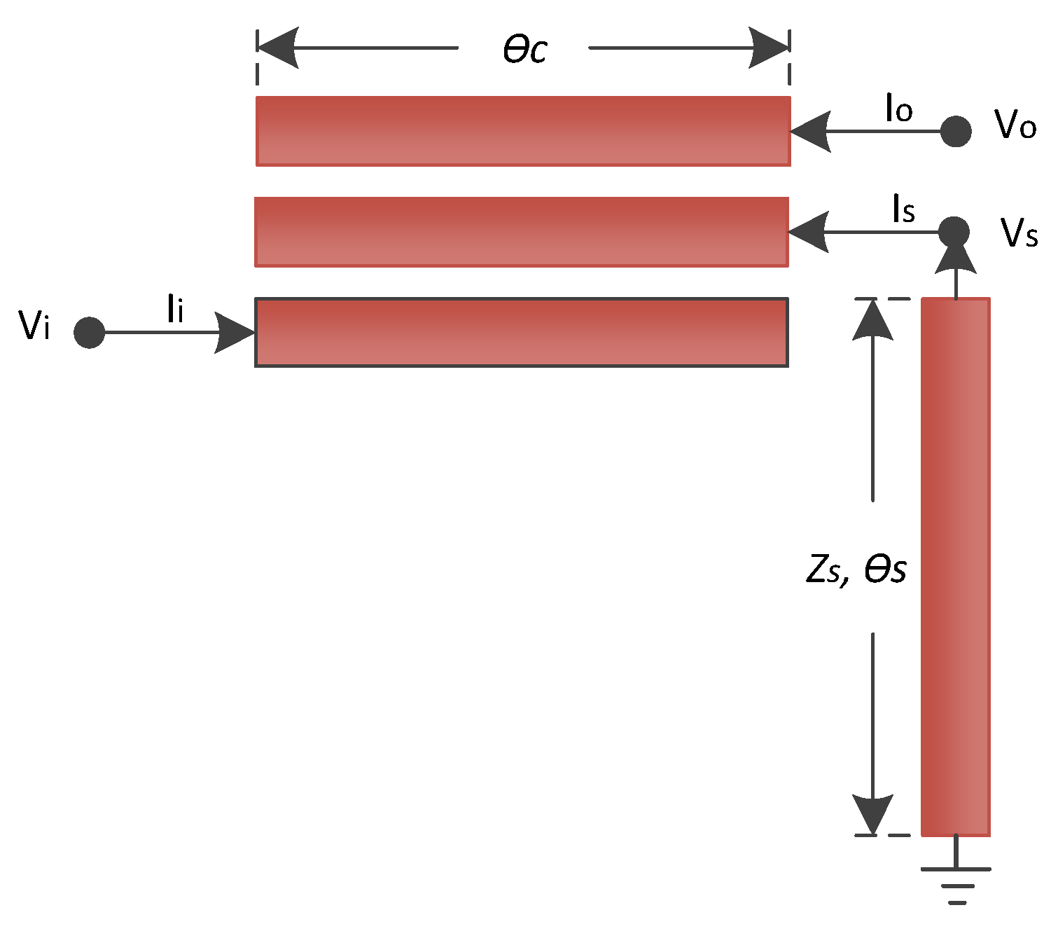
2. UWB Filter Design and Analysis

The proposed configuration of the microstrip wideband bandpass filter with a narrow notch using a microstrip line is illustrated in Figure 1. The wideband bandpass microstrip filter was designed using a single section of parallel-coupled lines with an electrical length ( θ c ) of a quarter-wavelength at the center frequency of the desired UWB passband. At the end of the central line of the coupled lines, a short-circuited stub was connected. The electrical length ( θ s ) of the short-circuited stub is a quarter-wavelength at the midband frequency of the desired passband (6.9 GHz). In addition, a stepped-impedance resonator was placed close to the three parallel lines section. The stepped-impedance resonator was designed to have a length of a half-wavelength at the mid-band frequency of the notch. A general six-port three parallel microstrip line configuration is shown in Figure 2.
The relationship of the port currents and voltages of the symmetrical three parallel-coupled lines can be described as follows:
d [ V ] dx = [ z ] [ I ]
where [ I ] and [ V ] are the three-dimensional column vectors and [ z ]   is the 3 × 3 impedance matrix, which are defined by
[ z ] = [ z 11 z 12 z 13 z 12 z 22 z 12 z 13 z 12 z 11 ] ,       [ V ] = [ V 1 V 2 V 3 ] ,       [ I ] = [ I 1 I 2 I 3 ]
The eigenvalue equation for [ z ] can be written as follows:
( [ z ] λ [ E ] ) [ x ] = 0
where [ λ ] = λ [ E ] is a matrix whose diagonal elements are the eigenvalues of [ z ] , [ E ] is the unity matrix, and [ x ] is a matrix with columns denoting the eigenvalues of [ z ] . More details of the design equations of the parallel line are explained in [18,19].
The circuit model of the presented microstrip filter without a notch is depicted in Figure 3. From the six-port network expression in Figure 2, the circuit model in Figure 3 can be considered as a two-port network with the following termination conditions:
I 1 = I 2 = I 6 = 0
I i = I 3
I o = I 4
V i = V 3
V o = V 4
V s = I 5 ( j Z s t a n θ s )
Taking these conditions into account, the scattering parameters can be extracted as described in [20].
Following the procedure in [18,19,20], the characteristic impedances, admittances, and the length of the coupled three lines of equal width and separation using the defined microstrip substrate can be computed for the three normal modes taking into account the conditions in (4) to (9). The proposed microstrip filter was developed to attain a passband with a fractional bandwidth of 110% at a midband frequency of around 6.9 GHz to meet the FCC requirements for the UWB spectrum. It was developed and implemented on a low-cost microstrip substrate with a relative dielectric constant of 10.8. The thickness of the substrate ‘was chosen to be 1.27 mm. The microstrip configuration for the bandpass filter is presented in Figure 4. The microstrip physical length and width for the parallel lines are represented by L and W , respectively. The spacing between the coupled three lines is represented by g. The microstrip physical length and width for the short-circuited stub are represented by   L s and W s , respectively.
In order to attain a passband with a FBW of more than 110% at 6.9 GHz midband frequency, the physical sizes for the coupled line section were selected to be as follows: W = 0.1   mm , L = 3.9   mm , g = 0.05   mm . The width of the 50 Ω feedlines for the input and output ports was found to be   1.1   mm . The electromagnetic simulated behavior for the parallel lines section with and without short-circuited stub is demonstrated in Figure 5. It can be noticed that the three parallel lines section without adding the stub exhibited a passband with only a single transmission zero at the DC and a second transmission zero at double the midband frequency. For the purpose of enhancing the performance of this type of structure and to achieve a very high selectivity, more sections are required, which will increase the filter circuit size. Alternatively, a single shorted stub can be added at the end of the midline of the parallel lines section to exhibit two additional symmetric transmission zeros in the rejection bands and close to the passband boundaries as displayed in Figure 5. In order to locate the two transmission zeros at   2.6   GHz and at   11   GHz , the physical dimensions for the shorted stub parameters were selected as follows: W s = 0.4   mm , L s = 4.2   mm . As a result, an ultra-wideband passband with very high selectivity was obtained. The two transmission zeros not only increased the selectivity of the passband, but have also extended the rejection bands efficiently, as shown in Figure 5. At the upper rejection band, there is another additional transmission zero which is symmetrical to the transmission zero nearby the upper side of the passband. This transmission zero widened the upper rejection band effectively. Hence, the presented UWB filter with only one section of three parallel-coupled lines attained sharp passband skirts and wide rejection bands. As an advantage, the proposed filter achieved a very compact circuit size, which makes this filter attractive for filter design engineers.
In order to minimize the physical circuit size of the presented UWB microstrip filter, the short circuit stub was folded, and its length and width were optimized in such a way that does not cause any unwanted coupling with the parallel-coupled line. The final microstrip layout of the presented UWB filter with folded stub is displayed in Figure 6. Figure 7 demonstrates the simulated insertion loss (S21) and return loss (S11) of the proposed microstrip filter. The insertion loss was better than 25 dB at the lower rejection band and more than 15 dB at the upper rejection band. The return loss showed four poles inside the desired passband with more than −15 db. One advantage of adding the short-circuited stub is the control of the bandwidth of the bandpass filter. This can be achieved by changing the value of the characteristic impedance of the short-circuited stub without changing the other parameters of the coupled lines.
Figure 8 depicts the simulated insertion loss (S21) with different values of the characteristic impedance of the short-circuited stub. As demonstrated in Figure 8, the pair of transmission zeros at the lower and upper rejection bands can be generated at precise frequencies by changing the value of Z s .   As can be noticed, the bandwidth is directly proportional to the value of the characteristic impedance of the shorted stub where higher impedance provides larger bandwidth and vice versa. However, increasing the value of the shorted stub impedance reduced the insertion loss level at the out-of-band as can be seen in Figure 8. An additional advantage of the proposed filter is that the transmission zero at the upper rejection band can be also controlled by changing the shorted stub length ( L s ) as displayed in Figure 9. Therefore, different bandwidths can be obtained by only changing the short-circuited stub length ( L s ), where reducing ( L s ) shifts the upper transmission zero to a higher frequency, providing a larger bandwidth and vice versa. Those two advantages of the proposed structure provide more flexibility to tune and optimize the design for specific requirements.

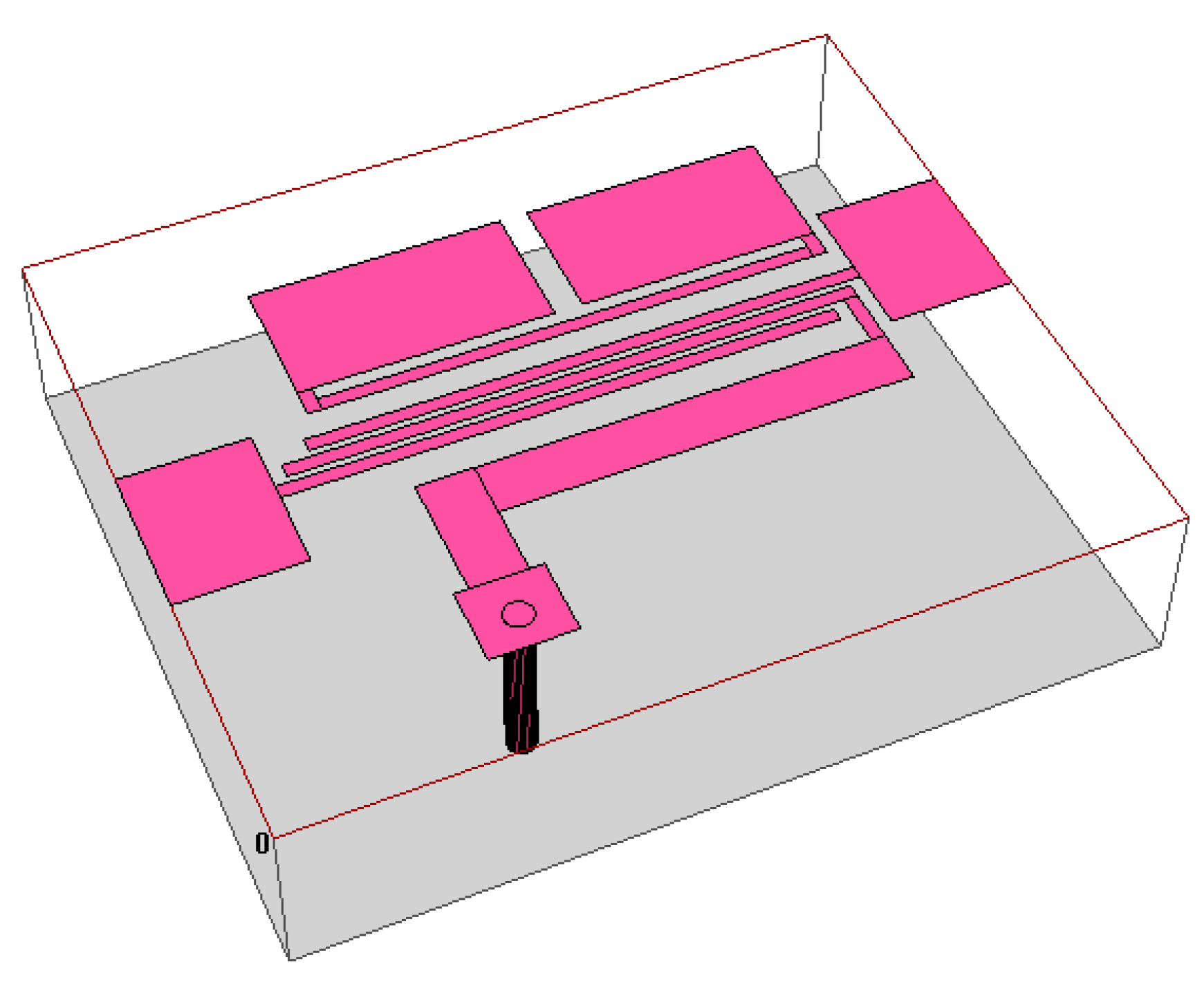
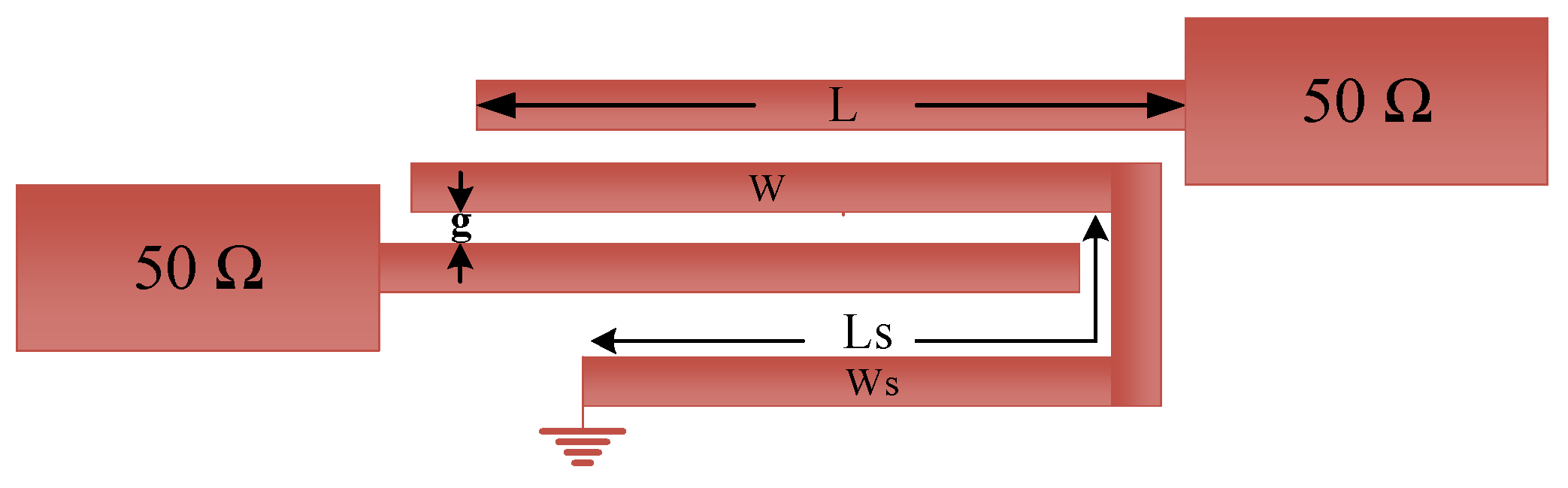
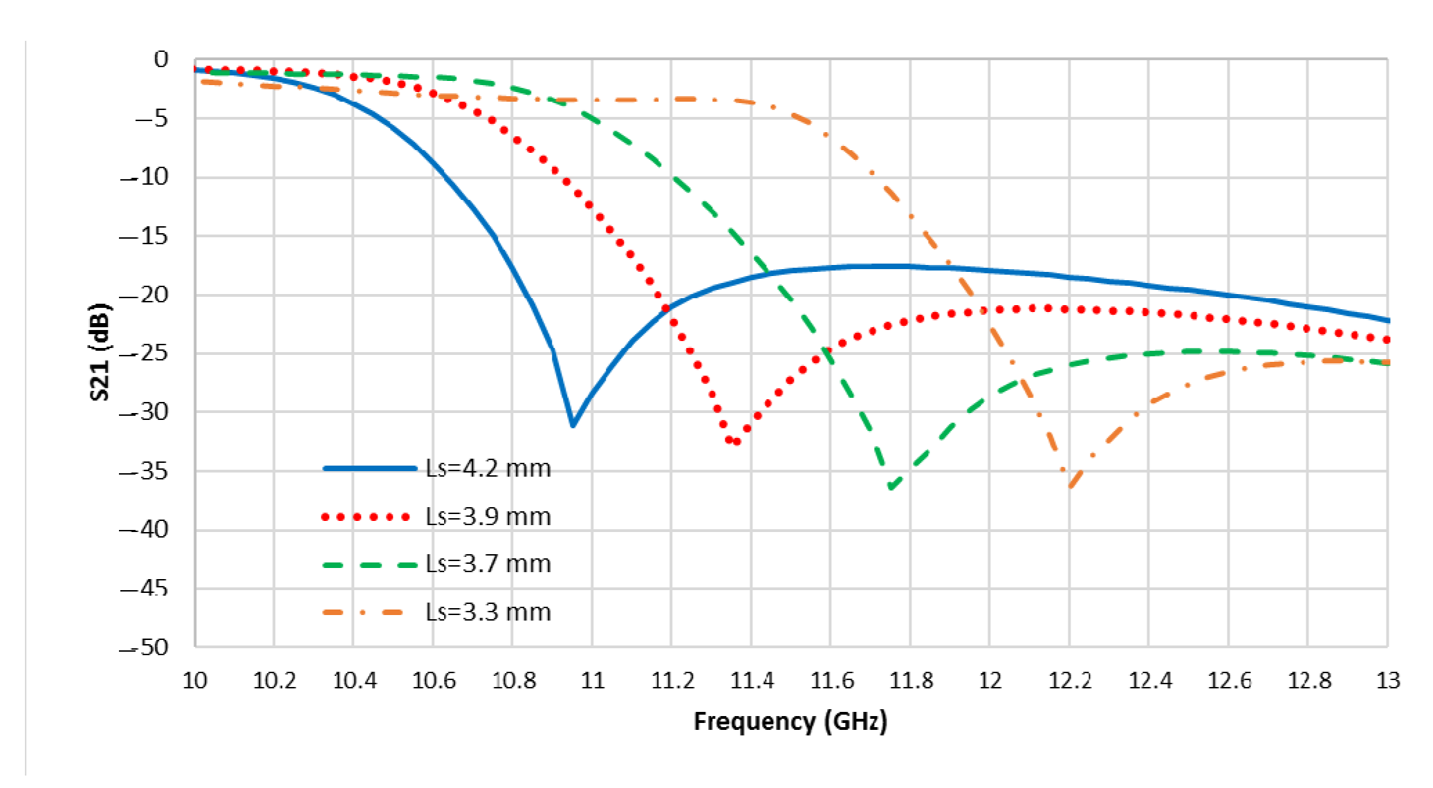
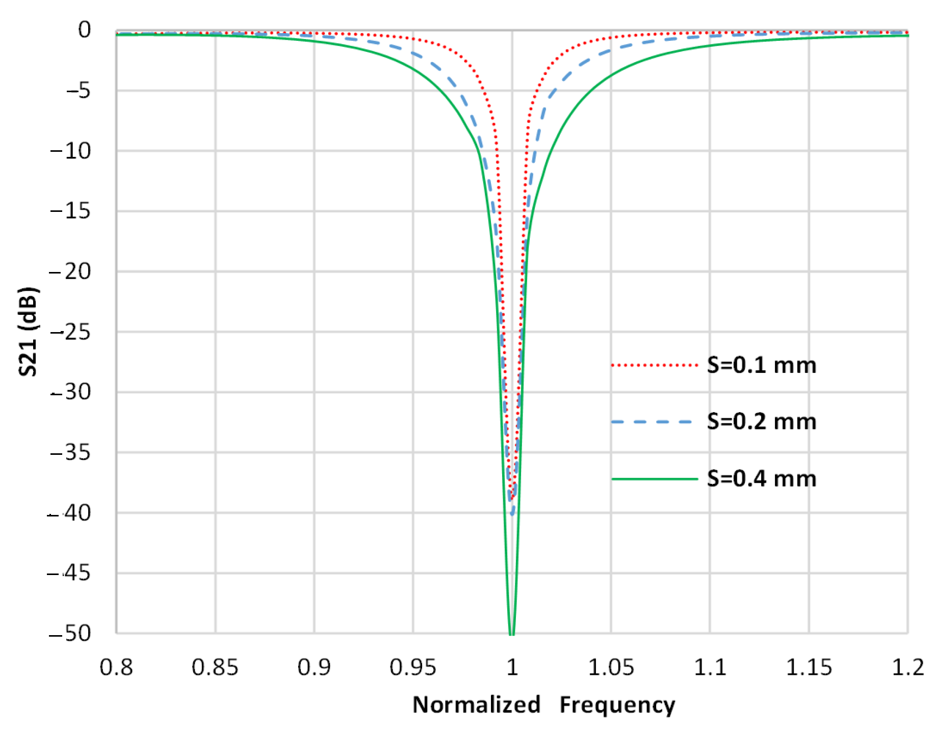
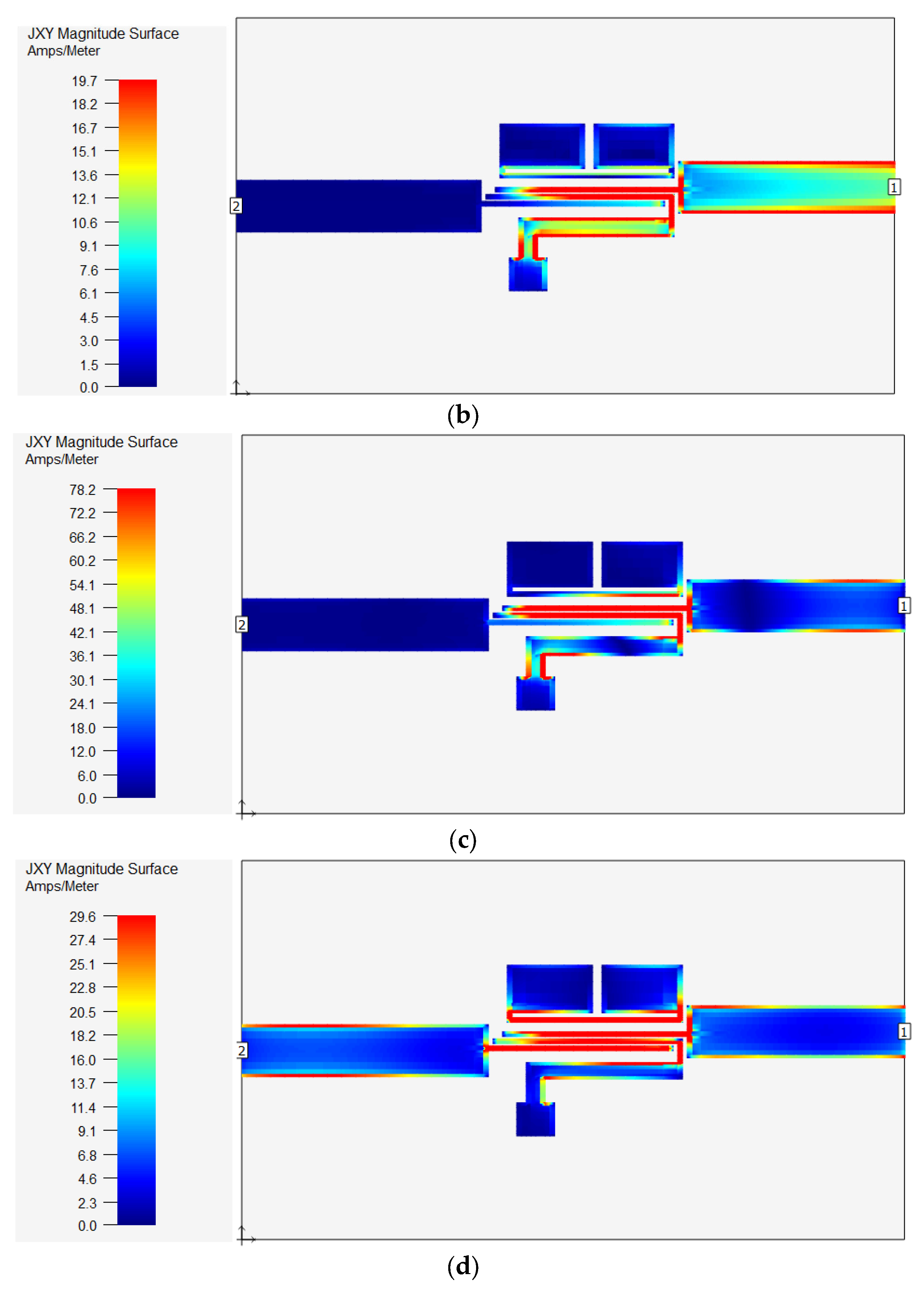
3. Implementation of Notched Filter

Since the specified UWB spectrum by the U.S. Federal communication commission covers a very large band, there are many existing radio signals with very narrow passbands that may produce interference with the UWB systems. Thus, the UWB bandpass filters should have the capability of rejecting those unwanted radio signals. To create a notched band filter to reject the unwanted radio signal that may appear inside the passband (such as a WLAN signal), a single stepped-impedance resonator was employed as illustrated in Figure 9. The stepped-impedance resonator contains two sections of low impedance separated by one element of high impedance. As demonstrated in Figure 10, the electrical length and the characteristic impedance of the low-impedance sections were defined by θ L and Z L . Moreover, the electrical length and the characteristic impedance of the high-impedance element were denoted by θ H and   Z H , respectively. In order to determine the resonance frequencies of the stepped-impedance resonator, the following conditions should be met [21]:
θ 0 = t a n 1 K
where the impedance ratio of the stepped-impedance resonator is denoted by K and can be defined by ( K = Z L / Z H ). The entire electrical length for the stepped-impedance resonator is defined as follows:
θ S I R = 2 ( θ L + θ h ) = π / 2
The impedance ratio K can be used to control the fundamental frequency and spurious resonance mode for the stepped impedance. For instance, when   θ H = θ L = θ 0 , the primary as well as the first spurious resonant frequencies ( f 0 ) and ( f s 1 ) are expressed as follows:
f s 1 = [ π t a n 1 K ] f 0
Figure 11 illustrates the microstrip layout of the UWB filter with a notched band. The length and width of the high-impedance part of the stepped-impedance resonator are defined by     L h and   W h . In addition, the physical length and width of the low-impedance sections are represented by   L L and by W L , respectively. In order to produce the notch at a midband frequency (   f 0 ) of around 6.3 GHz to block the unwanted WLAN signal, the physical parameters for the stepped-impedance resonator were chosen to be as follows: W L = 0.95   mm ,     L L = 1.7   mm , W h = 0.1 mm,   L h = 4.1   mm . The stepped-impedance resonator was folded for circuit size reduction as shown in Figure 11.
Figure 12 depicts the EM-simulated performance (insertion loss) of the notched filter. The bandwidth of the notch can be controlled by the spacing (s) between the stepped-impedance resonator and the parallel lines section, as demonstrated in Figure 12. As can be noticed that the bandwidth is directly proportional to the spacing (s), which means increasing the spacing (s) extends the bandwidth and vice versa. For the purpose of producing a narrow notched band that has a fractional bandwidth (FBW) of approximately 5% at a 6.3 GHz mid-band frequency, the spacing (s) was selected to be 0.2 mm. The EM-simulated insertion (S21) and return (S11) losses of the microstrip layout, shown in Figure 11, for the presented bandpass filter with a notched band, is displayed in Figure 13. The presented filter exhibits a UWB passband with high selectivity, notched band, and wideband stopbands. Figure 14 demonstrates the current density of the proposed filter at the transmission zeros, the notched band frequency, and the center frequency of the UWB passband. It can be noticed from the current distribution in Figure 14 that there was no transmission at the transmission zeros frequencies and the notched frequency.

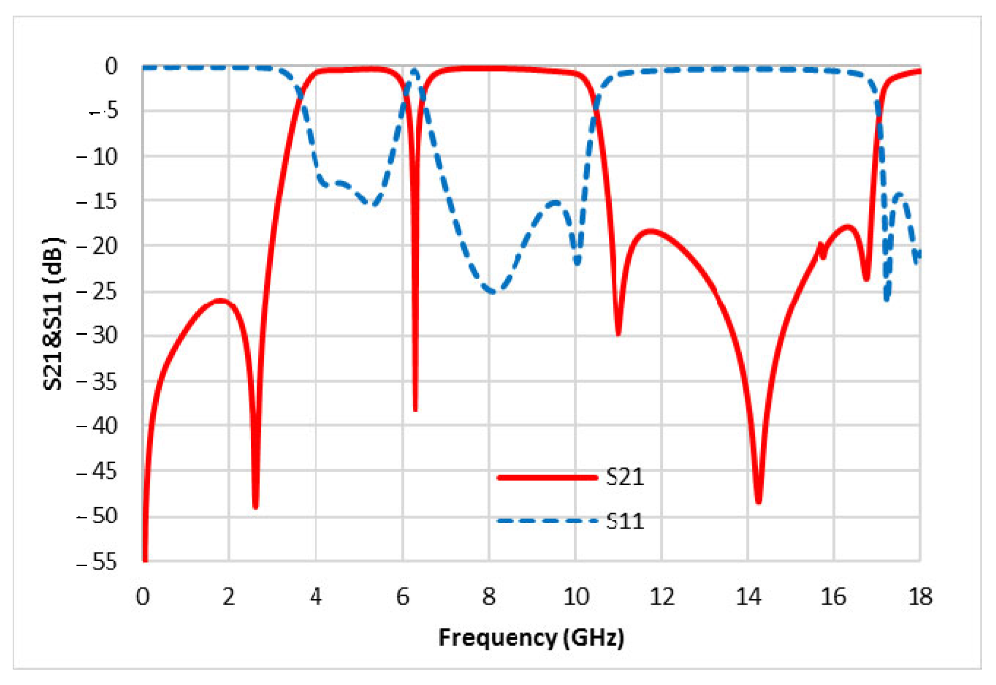
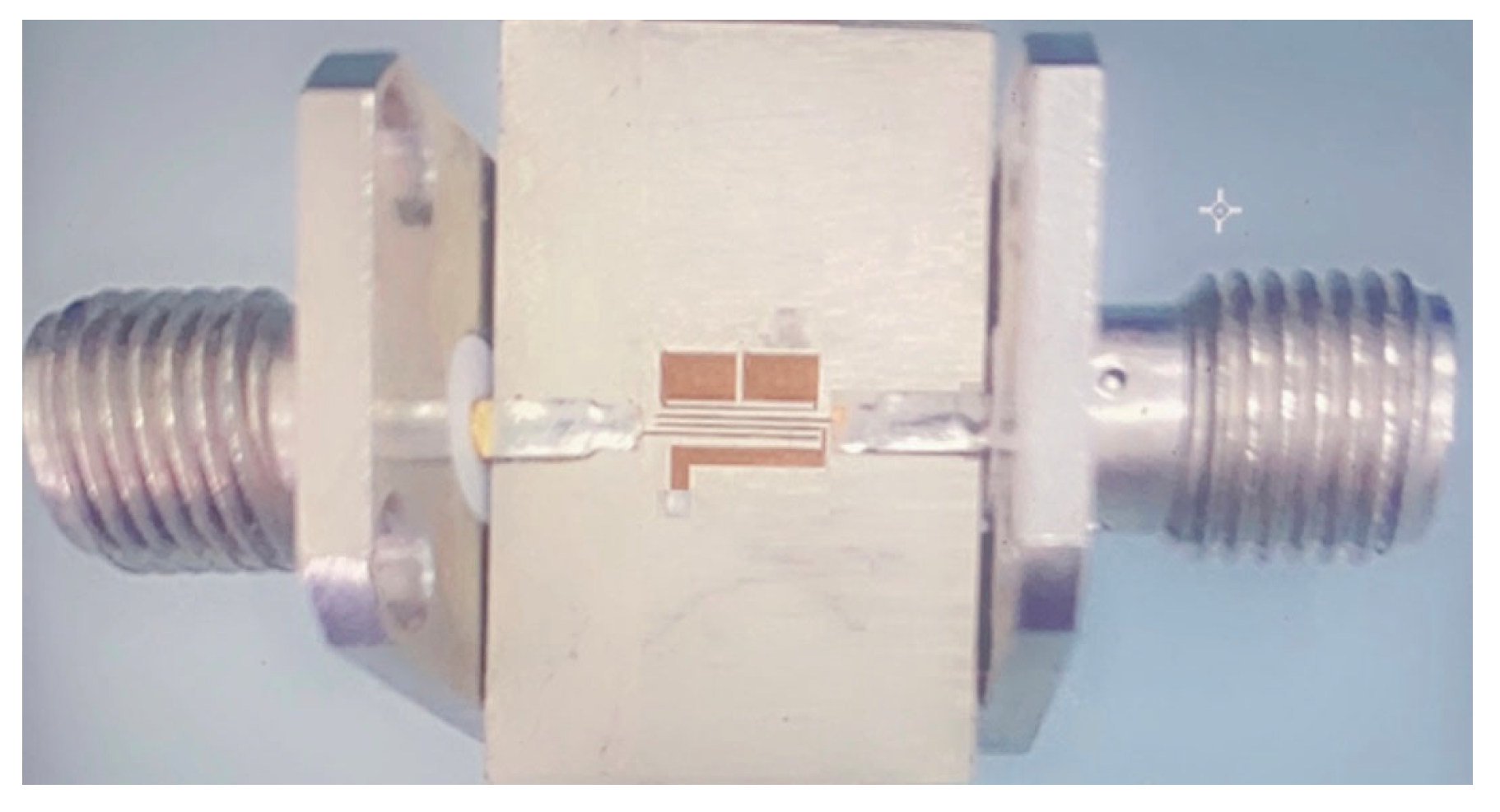
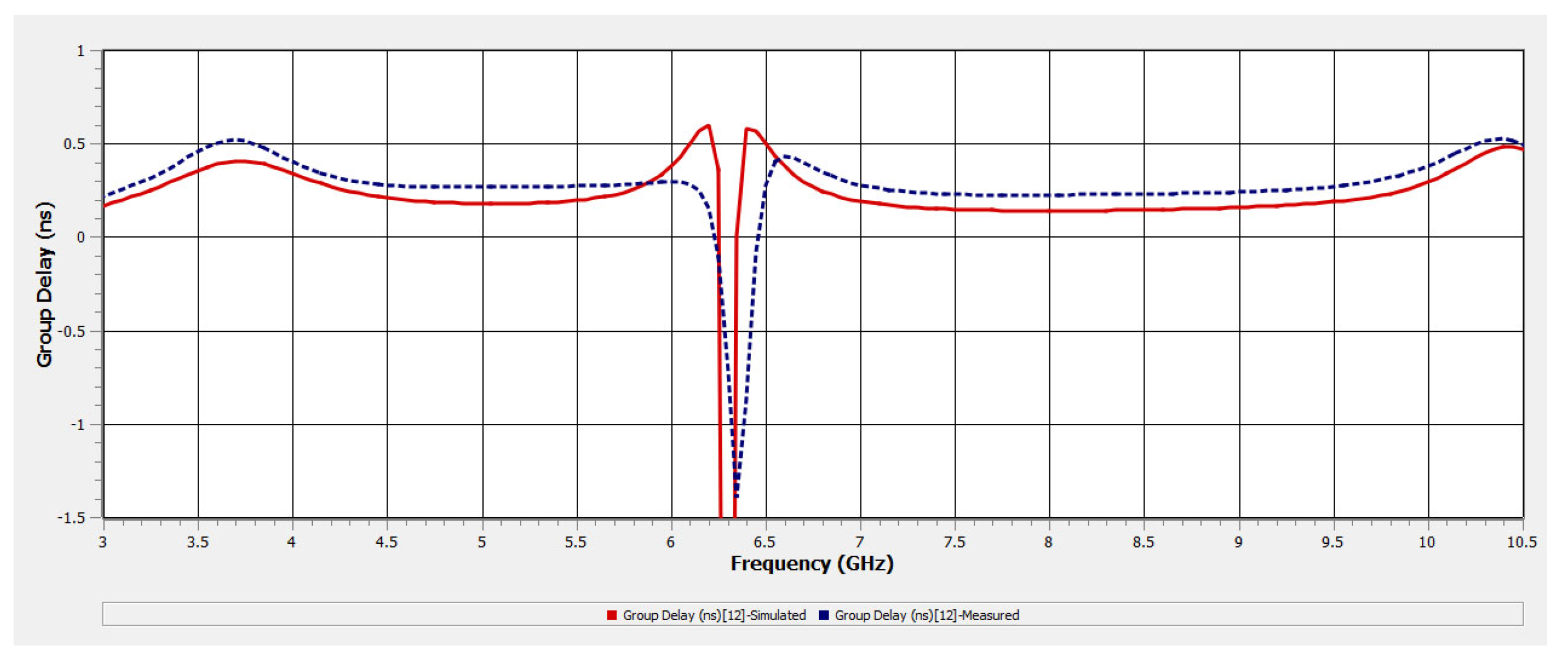
4. Fabrication and Measurements

The presented bandpass filter with a notch was designed utilizing a microstrip substrate with a 10.8 relative dielectric constant. The thickness for the microstrip substrate was chosen to be 1.27 mm. The filter design was successfully manufactured using printed-circuit-board technology. Figure 15 depicts a photograph of the fabricated filter. In addition, pairs of SMA 212-500SF connectors were attached at the input/output feedlines to allow the measurement of the scattering parameters (S11 and S21). The overall size of the manufactured microstrip filter with a notch was very small, with a physical size of 3.5 mm × 4.2 mm. A comparison between the measured and EM-simulated insertion and return losses is demonstrated in Figure 16 for the developed UWB microstrip filter with a notch. As can be seen in Figure 16, an outstanding agreement was attained among the expected and experimented insertion and return losses. In addition, the filter showed a very wide passband with a FBW of around 110% at a midband frequency of nearly 6.9 GHz. The fabricated filter showed an insertion loss with a very high selectivity and with a couple of transmission zeros near the passband edges. The measured insertion loss is recorded to be very low with a maximum value of 0.9 dB over the whole passband. Moreover, the measured return loss was recorded with a minimum value of 12 dB within the passband. The measured filter displayed an excellent out-of-band performance with rejection levels of more than 25 dB at the lower band and more than 18 dB at the upper band. In addition, the fabricated filter exhibited a notch with a narrow band, which has a fractional bandwidth of around 4.3% at a mid-band frequency of about 6.3 GHz, inside the passband. The rejection level of the insertion loss was better than 20 dB at the center frequency of the notched band. The filter exhibited a flat group delay of less than 0.4 ns at the midband frequency of each passband, as demonstrated in Figure 17. Table 1 provides a comparison with other reported filters [2,3,4,5,6,7,8]. The proposed UWB bandpass filter showed a very small circuit size compared to those filters which are presented in [2,3,4,5,6,7,8]. It also showed an excellent performance with a very low insertion loss compared to those filters in [2,3,4,5,6,7]. In addition, the return loss of the proposed filter was better than 12 dB inside the desired passband, which is better than the return loss of the filters in [3,5,6,7,8].

5. Conclusions

This article introduced a compact microstrip parallel-coupledcoupled-line bandpass filter with an ultra-wideband (UWB) passband and a narrow notched band. The presented UWB bandpass filter was developed by using three parallel-coupled-line sections. The electrical length of the coupled lines was designed to be a quarter-wavelength at approximately 6.9 GHz midband frequency. A very high selectivity was achieved using additional short-circuited stubs, which generated a transmission zero at the lower and upper rejection bands close to the desired UWB passband edges. In order to generate a notch with a narrow band inside the passband to reject the unwanted WLAN signal, a stepped-impedance resonator was coupled to the three parallel-coupled line sections. The fabricated filter showed an excellent agreement between the measured and the full-wave electromagnetic simulated performances. The measured insertion loss was very low along the entire UWB passband. The fabricated UWB filter is very compact compared to other filters in the literature.

Author Contributions

Conceptualization, G.H.A., F.H.A. and H.N.S.; methodology, G.H.A. and F.H.A.; software, G.H.A. and F.H.A.; analysis, G.H.A., F.H.A. and H.N.S.; validation, G.H.A. and H.N.S.; formal analysis, F.H.A., G.H.A. and H.N.S.; fabrication, G.H.A., F.H.A. and H.N.S.; measurement, G.H.A., F.H.A. and H.N.S.; investigation, G.H.A. and H.N.S.; resources, F.H.A. and G.H.A.; data curation, F.H.A. and G.H.A.; writing—original draft preparation, F.H.A. and G.H.A.; writing—review and editing, F.H.A. and H.N.S.; visualization, F.H.A. and G.H.A.; supervision, H.N.S.; project administration, H.N.S. All authors have read and agreed to the published version of the manuscript.

Funding

This research received no external funding.

Conflicts of Interest

The authors declare no conflict of interest.

References

  1. FCC. Revision of Part 15 of the Commission’s Rules Regarding Ultra-Wide-Band Transmission System; First Note and Order Federal Communication Commission, ET-Docket 98-153; FCC: Washington, DC, USA, 2002. [Google Scholar]
  2. Hameed, M.; Xiao, G.; Qiu, L.; Xiong, C.; Hameed, T. Multiple-Mode Wideband Bandpass Filter Using Split Ring Resonators in a Rectangular Waveguide Cavity. Electronics 2018, 7, 356. [Google Scholar] [CrossRef] [Green Version]
  3. Zhu, L.; Sun, S.; Menzel, W. Ultra-wideband (UWB) bandpass filters using multiple-mode resonator. IEEE Microw. Wirel. Compon. Lett. 2005, 15, 796–798. [Google Scholar]
  4. Li, R.; Zhu, L. Compact UWB bandpass filter using stub-loaded multiple-mode resonator. IEEE Microw. Wirel. Compon. Lett. 2007, 17, 40–42. [Google Scholar] [CrossRef]
  5. Wong, S.; Zhu, L. Quadruple-mode UWB bandpass filter with improved out-of-band rejection. IEEE Microw. Wirel. Compon. Lett. 2009, 19, 152–154. [Google Scholar] [CrossRef]
  6. Deng, H.; Zhao, Y.; Zhang, L.; Zhang, X.; Gao, S. Compact quintuple-mode stub-loaded resonator and UWB filter. IEEE Microw. Wirel. Compon. Lett. 2010, 20, 438–440. [Google Scholar] [CrossRef]
  7. Chu, Q.; Tian, X. Novel UWB bandpass filters using stub-loaded multiple-mode resonator. IEEE Microw. Wirel. Compon. Lett. 2011, 21, 403–405. [Google Scholar] [CrossRef]
  8. Qian, K.W.; Tang, X.H. Compact Ultra-Wideband Low-Temperature Co-Fired Ceramic Bandstop Filter Using Semi-Lumped Resonators. Electromagnetics 2012, 32, 193–199. [Google Scholar] [CrossRef]
  9. Shaman, H.; Almorqi, S.; AlAmoudi, A. Ultra-wideband (UWB) Bandpass Filter with Cascaded Lowpass Filter on Multilayer Liquid-Crystal Polymer (LCP) Substrate. IETE J. Res. 2016, 62, 63–67. [Google Scholar] [CrossRef]
  10. Li, C.; Ma, Z.; Chen, J.; Wang, M.; Huang, J. Design of a Compact Ultra-Wideband Microstrip Bandpass Filter. Electronics 2023, 12, 1728. [Google Scholar] [CrossRef]
  11. Jamsai, M.; Angkawisittpan, N.; Nuan-On, A. Design of a Compact Ultra-Wideband Bandpass Filter Using Inductively Compensated Parallel-Coupled Lines. Electronics 2021, 10, 2575. [Google Scholar] [CrossRef]
  12. La, D.-S.; Guan, X.; Chen, S.-M.; Li, Y.-Y.; Guo, J.-W. Wideband Band-Pass Filter Design Using Coupled Line Cross-Shaped Resonator. Electronics 2020, 9, 2173. [Google Scholar] [CrossRef]
  13. Huang, L.; Zhang, S. Ultra-Wideband Ridged Half-Mode Folded Substrate-Integrated Waveguide Filters. IEEE Microw. Wirel. Compon. Lett. 2016, 28, 579–581. [Google Scholar] [CrossRef]
  14. Razzaz, F.; Saeed, S.; Alkanhal, M. Ultra-Wideband Bandpass Filters Using Tapered Resonators. Appl. Sci. 2022, 12, 3699. [Google Scholar] [CrossRef]
  15. Liu, L.-Q.; Lai, H.-S.; Hu, H.-M.; Chen, J.-J.; Weng, M.-H.; Yang, R.-Y. A Simple Method to Design a UWB Filter with a Notched Band Using Short-Circuit Step Impedance Stubs. Electronics 2022, 11, 1124. [Google Scholar] [CrossRef]
  16. Shaman, H.; Hong, J.-S. Ultra-Wideband (UWB) bandpass filter with embedded band notch structures. IEEE Microw. Wirel. Compon. Lett. 2007, 17, 193–195. [Google Scholar] [CrossRef]
  17. Zheng, X.; Pan, Y.; Jiang, T. UWB Bandpass Filter with Dual Notched Bands Using T-Shaped Resonator and L-Shaped Defected Microstrip Structure. Micromachines 2018, 9, 280. [Google Scholar] [CrossRef] [PubMed] [Green Version]
  18. Pavlidis, D.; Hartnagel, H. The design and performance of three-line microstrip couplers. IEEE Trans. Microw. Theory Tech. 1976, 24, 631–640. [Google Scholar] [CrossRef]
  19. Tripathi, V. On the analysis of symmetrical three-line microstrip circuits. IEEE Trans. Microw. Theory Tech. 1977, 25, 726–729. [Google Scholar] [CrossRef]
  20. Pozar, D.M. Microwave Engineering, 2nd ed.; John Wiley: New York, NY, USA, 1998. [Google Scholar]
  21. Makimoto, M.; Yamashita, S. Bandpass filters using parallel coupled stripline stepped impedance resonators. IEEE Trans. Microw. Theory Tech. 1980, 28, 1413–1417. [Google Scholar] [CrossRef]
Figure 1. Structure of the presented microstrip wideband bandpass filter with a notch.
Applsci 13 06834 g001
Figure 2. Schematic of six-port three parallel-coupled microstrip lines.
Applsci 13 06834 g002
Figure 3. Circuit model for the presented UWB filter without a notched band.
Applsci 13 06834 g003
Figure 4. Microstrip structure for the presented UWB bandpass filter.
Applsci 13 06834 g004
Figure 5. Frequency response for the three parallel lines section without and with shorted stubs.
Applsci 13 06834 g005
Figure 6. The microstrip layout of the presented UWB bandpass filter with a folded stub.
Applsci 13 06834 g006
Figure 7. Simulated performance of the filter without notched band: insertion (S21) and return (S11) losses.
Applsci 13 06834 g007
Figure 8. Simulated insertion loss (S21) with various values of the characteristic impedance.
Applsci 13 06834 g008
Figure 9. Simulated insertion loss (S21) with various lengths (Ls) of the short-circuited stub.
Applsci 13 06834 g009
Figure 10. The microstrip stepped-impedance resonator configuration.
Applsci 13 06834 g010
Figure 11. Microstrip layout for the filter with a notch.
Applsci 13 06834 g011
Figure 12. EM-simulated performance of the notch with various values of the spacing (s).
Applsci 13 06834 g012
Figure 13. EM-simulated insertion (S21) and return (S11) losses of the UWB bandpass microstrip filter with a notched band.
Applsci 13 06834 g013
Figure 14. Current distributions at (a) the notched frequency, (b) the lower transmission zero, (c) the upper transmission zero, and (d) the center frequency of the UWB passband: (1 and 2 represent Port 1 and Port 2).
Applsci 13 06834 g014aApplsci 13 06834 g014b
Figure 15. A photograph of the fabricated filter.
Applsci 13 06834 g015
Figure 16. Comparison between full-wave EM-simulated and measured insertion and return losses for the presented filter with a notch: (a) (S21) and (b) (S11).
Applsci 13 06834 g016aApplsci 13 06834 g016b
Figure 17. Comparison between the group delay of the simulated and measured filter.
Applsci 13 06834 g017
Table 1. Results comparison with other UWB filters.
Ref.Passband (GHz)FBW (%)S11 (dB)S21 (dB) Circuit   Size   ( λ g × λ g )
[2]1.83–3.1653>14≤1.00.62 × 0.25
[3]2.96–10.67113>10≤2.00.35 × 0.05
[4]2.8–10.27112>14≤1.40.32 × 0.07
[5]2.8–11.0119>10≤1.10.22 × 0.16
[6]2.8–11.2120>12≤2.00.61 × 0.23
[7]3.1–11.1117>10≤1.50.51 × 0.34
[8]1.0–20.0180>10≤0.60.8 × 0.22
This work3.1–10.7110>12≤0.90.096 × 0.08
Disclaimer/Publisher’s Note: The statements, opinions and data contained in all publications are solely those of the individual author(s) and contributor(s) and not of MDPI and/or the editor(s). MDPI and/or the editor(s) disclaim responsibility for any injury to people or property resulting from any ideas, methods, instructions or products referred to in the content.

