Article

Sliding Mode Regulation of a Boost Circuit for DC-Biased Sinusoidal Power Conversion

by
Jorge Rivera
1,*,
Susana Ortega-Cisneros
1,*,
Julio C. Rosas-Caro
2,* and
Omar-Fernando Ruíz-Martínez
3,*
1
Department of Electronic System Design, Centro de Investigación y de Estudios Avanzados del Instituto Politécnico Nacional, Zapopan 45017, Jalisco, Mexico
2
Facultad de Ingeniería, Universidad Panamericana, Alvaro del Portillo 49, Zapopan 45010, Jalisco, Mexico
3
Faculty of Engineering, Universidad Panamericana, Josemaria Escriva de Balaguer 101, Aguascalientes 20290, Mexico
*
Authors to whom correspondence should be addressed.
Appl. Sci. 2023, 13(10), 5963; https://doi.org/10.3390/app13105963
Submission received: 23 March 2023 / Revised: 30 April 2023 / Accepted: 4 May 2023 / Published: 12 May 2023
(This article belongs to the Special Issue Research and Development on DC-DC Power Converters)

Abstract

:
The boost converter is mostly used as a DC–DC converter, but two boost converter power stages can be configured to perform the DC–AC conversion. In this case, the control system of the power stage must be designed for trajectory tracking (instead of regulation), which brings interesting challenges. This work deals with the design of a higher-order sliding mode output regulator for a DC-biased sinusoidal power conversion problem on a single boost converter stage of a boost inverter for asymptotic trajectory tracking of the voltage capacitor. The steady-state reference signal for the inductor current is proposed as an approximated solution of the well-known Francis–Isidori–Byrnes equations. The used approach is the direct control of the output, where the nonminimum phase variable, i.e., an adequate sliding function, stabilizes the current through the inductor. Lastly, by means of real-time experimentation, the good performance of the proposed control strategy is verified.

1. Introduction

Voltage source inverters (VSI) are among the most important power electronic circuits used in a variety of applications, including renewable energy systems, electric drives, and motor control. A VSI is a power electronic device that converts a DC voltage input into a variable-frequency and -amplitude AC output [1,2,3].
Voltage source inverters (buck inverters) generate an AC output instantaneous voltage always lower than their DC input [1,2,3]. When a larger voltage is required, a boost stage is required between the DC input and the buck inverter depending on the power level required; this option is a feasible solution, but the additional intermediate converter increases the cost and volume of the total system, as well as reduces the total efficiency. This is why the development of boost-type inverters is an active research field [4,5,6,7,8,9,10,11,12,13,14,15,16,17,18,19,20,21,22,23,24,25,26].
One of the main topologies of boost-type inverters is the differential boost inverter, sometimes simply called the boost inverter, initially introduced in [4]. This converter gained significant attention from researchers in the following decades due to its ability to overcome the limitations of the conventional full-bridge inverter, which is well-established. Specifically, the DC–AC boost converter can generate AC voltages with amplitudes greater than the input DC voltage without requiring an additional conversion stage or increasing the number of power semiconductors.
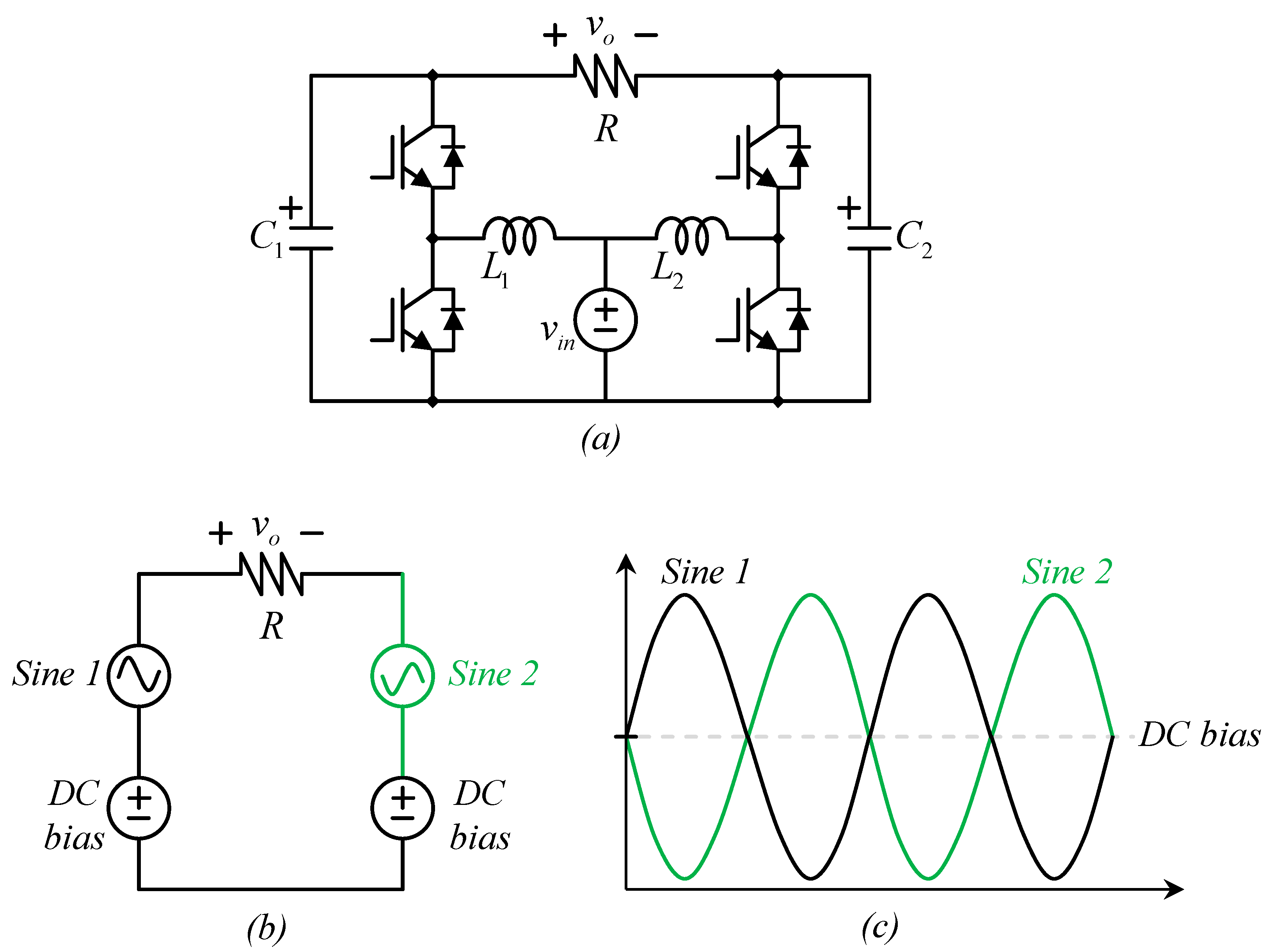
Figure 1a shows the discussed converter, which is made up of two identical cells that use symmetrical converters. The cells are connected back-to-back or in a bridge configuration, providing the output voltage differentially between their outputs. The converter can be divided into two single boost converters, each of them generating a DC-biased sinusoidal voltage; see the simplified diagram in Figure 1b. The DC bias is introduced since the boost converter cannot produce a voltage lower than its input. It is the same value for both converters, as the load is connected in a differential manner; this DC value is not reflected on the output. This can also be observed by applying Kirchhoff’s voltage law (KVL) to the diagram of Figure 1b. From Figure 1b, it is also evident the DC bias must be the same in both converters to prevent a DC bias at the output voltage, which is expected to be an AC signal. Furthermore, sinusoidal signals generated by each boost converter must be shifted by 180°. In this case, these amplitudes are added at the output side (see Figure 1c).
One of the more interesting challenges in the boost converter is its control; it is a nonminimum phase system, which means that its linearized model has a right-half plane zero in the transfer function. Nevertheless, control can be performed, and it is widely used for regulation purposes. An example can be found in Appendix A. Another manner is to use an indirect method. Instead of directly controlling the capacitor’s voltage, which makes the inductor current an unstable variable, the inductor current may be directly controlled with a reference chosen to obtain a certain capacitor’s voltage (see Appendix B). Additionally, the boost inverter requires a trajectory tracking control which is more complex than the regulation-oriented control. These challenges require the use of advanced control techniques to achieve reliable and robust performance [10,11,12,13,14,15,16,17,18,19,20,21,22,23,24,25,26].
Among the different strategies of control applied to the boost inverter, the sliding mode control is one of the most investigated, and it has been widely recognized as an effective control strategy for power converters, including power boost converters. Sliding mode control has several advantages when applied to power boost converters, such as robustness to parameter variations and disturbances, fast transient response, and insensitivity to nonlinearities. Additionally, sliding mode control can precisely control the output voltage and current, making it well-suited for applications requiring high accuracy and efficiency.
Several applications have been reported for converters controlled with sliding-mode-based controllers. For example, in [20], a high-gain SMC algorithm was designed for the power flow regulation of a bidirectional converter; in [21], a generalized super-twisting algorithm was designed to control a DAB converter. Overall, sliding mode control offers a promising approach to achieving accurate and efficient control of power boost converters in various power electronics applications [20,21,22,23,24,25,26].
In this work, a direct control approach is used to solve the problem of tracking a DC-biased sinusoidal signal for the capacitor voltage on a DC–DC boost converter. This approach is based on a robust higher-order sliding mode output regulation technique based on the super-twisting algorithm. The unstable zero dynamics related to the inductor current variable are stabilized with a properly selected sliding surface. The reference signal chosen for the current through the inductor is an approximate solution to the corresponding Francis–Isidori–Byrnes equation.
The article is organized in the following manner: Section 1 presents the introduction, and Section 2 presents the model of the DC–Dc boost converter and the design of its output regulator based on a higher-order sliding mode controller. Then, Section 3 deals with the experiments performed to verify its performance. Lastly, Section 4 presents the conclusions.

2. Higher-Order Sliding Mode Regulation for Boost Converter Output

As observed in Figure 1, controlling the converter consists of controlling two converters that have the same parameters and work in the same manner. They are both boost converters generating a DC-biased sinusoidal signal. For this reason, the main focus of the problem is controlling a boost converter and forcing it to produce a sinusoidal DC-biased signal.
This chapter introduces the mathematical model of the DC–DC boost converter, as well as the formulation of the problem. Then, the higher-order sliding mode output regulation technique is used to design a controller for the formulated problem.

2.1. Mathematical Model and Problem Formulation for the Boost Converter

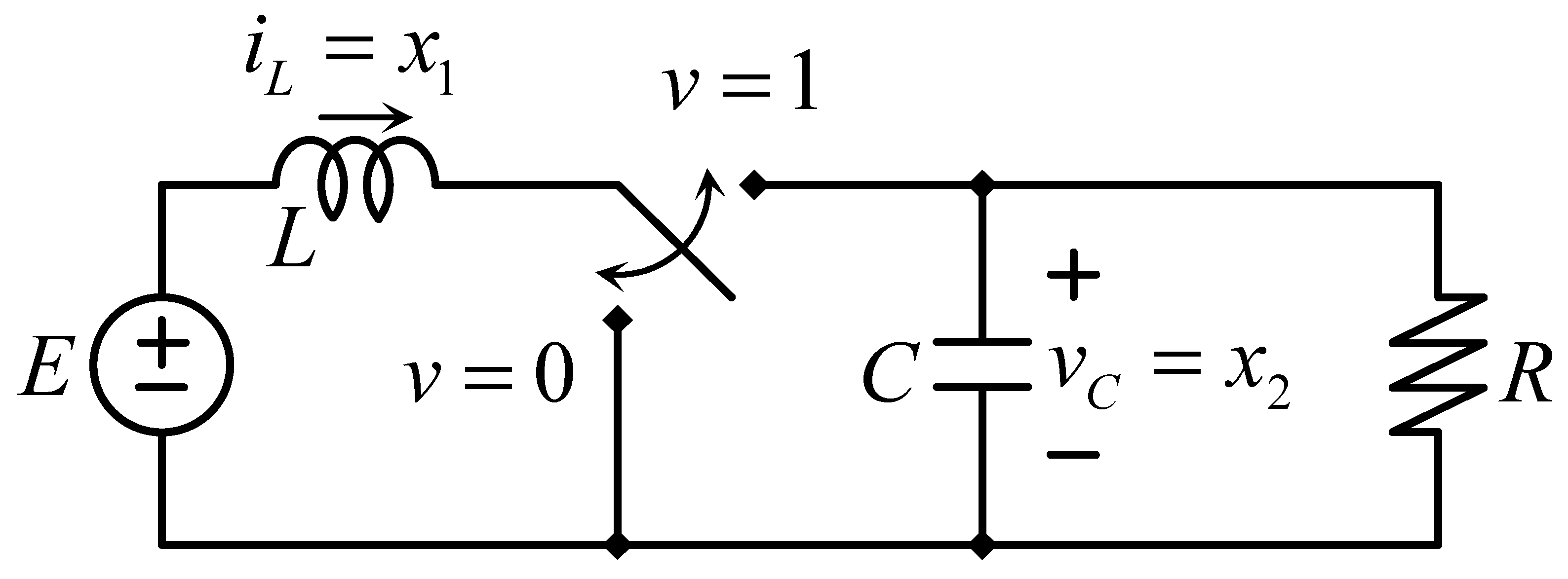
Figure 2 shows an electric diagram of a boost converter.
Using the standard averaging technique, the boost converter mathematical model can be expressed as follows [27]:
x ˙ 1 = x 2 L v + E L ,
x ˙ 2 = x 1 C v x 2 R C ,
y = x 2 ,
where x1 is the current through the inductor, and x2 is the voltage across the capacitor. The control signal v is the transistor switching function, a binary signal which can take values of 0 and 1, and whose value represents the instantaneous position of the transistor (see Figure 2). Moreover, E is the DC input voltage. The output resistance R, the inductance L and the capacitance C are considered constant parameters.
The control problem can be established by forcing the output y = x2 to track the variable reference signal x2,r in the presence of perturbations such as load resistance variations.
Now, let us consider the autonomous exosytem described by Equation (4).
ω ˙ 1 = α ω 2 ,     ω ˙ 2 = α ω 1 ,     ω ˙ 3 = 0 ,
with initial conditions w1(0) = w2(0) = a and w3(0) = b, and output
x 2 , r = q ( ω ) = ω 1 + ω 3 ,
where w1 is a sinusoidal shape signal whose amplitude is the square root of two and whose frequency is equal to α; w3 is a DC (constant) signal equal to b, which gives the bias value. Moreover, w = (w1, w2, w3)T. Lastly, the output tracking error is defined as
e = x 2 x 2 , r .

2.2. Higher-Order Sliding Mode Regulation of a Boost Power Converter

In the below procedure, it is assumed that the load resistance is known, along with the remaining plant parameters. Now, let us define the steady state error as
z = x π ( ω ) = ( z 1 , z 2 ) T ,
where x = (x1, x2)T and π(w) = (π1(w), π2(w))T. Then, the dynamic expression for Equation (7) with the tracking error in Equation (6) can be obtained from Equations (1)–(3) as follows:
z ˙ 1 = z 2 + π 2 ( ω ) L v + E L π 1 ( ω ) ω S ω ,
z ˙ 2 = z 1 + π 1 ( ω ) C v z 2 + π 2 ( ω ) R C π 2 ( ω ) ω S ω ,
ω ˙ = S ω ,
e = z 2 + π 2 ( ω ) q ( ω ) ,
where
S = [ 0 α 0 α 0 0 0 0 0 ] .
The smooth mappings π1(w): W0 and π2(w): W0 (where W0 is an open neighborhood of w = 0), with π1(0) = 0 and π2(0) = 0, are such that the pair (π1(w), π2(w)) is the unique solution of the following PDEs (FIB equations [28]):
π 1 ( ω ) ω S ω = π 2 ( ω ) L c ( ω ) + E L ,
π 2 ( ω ) ω S ω = π 1 ( ω ) C c ( ω ) π 2 ( ω ) R C ,
0 = π 2 ( ω ) q ( ω ) ,
where c(w) is the steady state for input v (as in the classical output regulation setting), which is deduced later on.
Remark 1.
Comparing Equations (15) and (5), it may come to our attention that ω1 + ω3 ≠ π2(ω). The control problem (posed in Section 2.1) stated that x2,r is the reference signal for the output of the system. This reference is proposed by the end user as in Equation (5), i.e., as a function of the state of the exosystem, i.e., q(ω), particularly depending on the summation of the states ω1 and ω3. The output error is then defined as e in Equation (11). For that, one calculates
e = y x 2 , r ,
e = x 2 x 2 , r ,
e = z 2 + π 2 x 2 , r ,
e = z 2 + π 2 q ( ω ) .
The FIB Equations (13)–(15) are determined under the assumption that the state of the system corresponds exactly to the ideal steady state, i.e., that all errors are zero. Hence, it is assumed that z1 = z2 = e = 0, yielding Equation (15).
Now, we introduce the sliding function σ that stabilizes the unstable residual dynamics, as well as the super-twisting controller [29], as follows:
σ = z 2 + c 1 z 1 ,
v = ( k 1 | σ | s i g n ( σ ) + v 1 ) / δ ( z , ω ) ,
v ˙ 1 = k 2 sign ( σ ) .
That leads to the closed-loop system,
σ ˙ = η ( z , ω ) k 1 | σ | sign ( σ ) + v 1 ,
v ˙ 1 = k 2 sign ( σ ) ,
where k1 and k2 as constant design parameters that are determined in Appendix C, with
η ( z , ω ) = c 1 E L c 1 π 1 ( ω ) ω S ω z 2 + π 2 ( ω ) R C π 2 ( ω ) ω S ω ,
δ ( z , ω ) = z 1 + π 1 ( ω ) C c 1 z 2 + π 2 ( ω ) L .
Remark 2.
The pulse width modulation (PWM) is automatically generated by the DSP board; nevertheless, this PWM is implemented as usual, i.e., with the comparison of a triangular carrier c t r vs. the signal v, called the duty cycle in the PWM scheme. The PWM generator ensures that vpwm is always within the interval [0, 1] with a logical rule in which, if v>, vpwm = 1, and if v<, vpwm = 0.

2.3. Stability Analysis of the Sliding Mode

When the designed sliding mode happens, i.e., σ(t) = z2(t) + c1z1(t) = 0tts, the sliding mode dynamics are described by the following first-order system:
z ˙ 1 = z 2 + π 2 ( ω ) L v + E L π 1 ( ω ) ω S ω | z 2 = c 1 z 1 v = v e q ( z , ω ) ,
where the equivalent control veq is calculated from σ ˙ = 0 as follows:
σ ˙ = η ( z , ω ) + δ ( z , ω ) v e q ( z , ω ) = 0 ,
v e q ( z , ω ) = η ( z , ω ) δ ( z , ω ) .
This results in
z ˙ 1 = f 0 ( z 1 , ω ) ,
where
f 0 ( z 1 , ω ) = ( c 1 z 1 + π 2 ( ω ) L ) ( c 1 E L c 1 π 1 ( ω ) ω S ω c 1 z 1 + π 2 ( ω ) R C π 2 ( ω ) ω S ω z 1 + π 1 ( ω ) C c 1 c 1 z 1 + π 2 ( ω ) L ) + E L π 1 ( ω ) ω S ω .
Lemma 1.
Under the conditions in Equations (13) and (14), origin z1 = 0 is an equilibrium point of the sliding mode dynamics in Equation (30).
Proof. 
Assume that z1 = 0; then, the sliding mode dynamics in Equation (30) reduces to the following expression:
f 0 ( 0 , ω ) = ( π 2 ( ω ) L ) ( c 1 E L c 1 π 1 ( ω ) ω S ω π 2 ( ω ) R C π 2 ( ω ) ω S ω π 1 ( ω ) C c 1 π 2 ( ω ) L ) + E L π 1 ( ω ) ω S ω .
By substituting Equations (13) and (14) into Equation (32), after simple manipulations, one obtains that
f 0 ( 0 , ω ) = π 2 ( ω ) L c ( ω ) + π 2 ( ω ) L c ( ω ) = 0 .
Lemma 2.
The sliding mode dynamics equilibrium point z1 = 0 (30) is locally attractive if c1 is selected in a way that
a ¯ 11 a ¯ 12 c 1 = λ 1 < 0 ,
where
a ¯ 11 = a 11 b 1 ( a 21 + c 1 a 11 ) ( b 2 + c 1 b 1 ) ,     a ¯ 12 = a 12 b 1 ( a 22 + c 1 a 12 ) ( b 2 + c 1 b 1 ) ,
with
a 1 , j = f i x j | ( b 2 / ( R E ) , b ) ,     b i = f i v | ( b 2 / ( R E ) , b ) ,
where f1 and f2 are the right-hand sides of Equations (8)–(9), respectively.
Proof. 
The corresponding linear approximation of Equations (13) and (14) is as follows:
Π 1 S ω = R 1 ω + b 1 Γ ω ,
Π 2 S ω = R 2 ω + b 2 Γ ω ,
with
R 1 = a 11 Π 1 + a 12 Π 2 ,
R 2 = a 21 Π 1 + a 22 Π 2 ,
where
Π i = π i ( ω ) ω | ( 0 ) , Γ = c ( ω ) ω | ( 0 ) , i , j = 1 ,   2 .
Let us define the steady-state errors as z1 = x1 − Π1w and z2 = x2 − Π2w, where the corresponding dynamic equations are as follows:
z ˙ 1 = a 11 z 1 + a 12 z 2 + b 1 v + R 1 ω Π 1 S ω + ϕ 1 ( z , ω ) ,
z ˙ 2 = a 21 z 1 + a 22 z 2 + b 2 v + R 2 ω Π 2 S ω + ϕ 2 ( z , ω ) .
The sliding function dynamics (the function defined in Equations (20)–(22)) take the following form:
σ ˙ = a 21 z 1 + a 22 z 2 + b 2 v + R 2 ω Π 2 S ω , + c 1 a 11 z 1 + c 1 a 12 z 2 + c 1 b 1 v + c 1 R 1 ω c 1 Π 1 S ω + ϕ σ ( ) ,
with ϕσ(z,w) = ϕ2(z,w) + c1ϕ1(z,w). The equivalent control is calculated as a solution of σ ˙ = 0 :
v e q = 1 b 2 + c 1 b 1 ( a 21 z 1 + a 22 z 2 + R 2 ω Π 2 S ω ) , 1 b 2 + c 1 b 1 ( + c 1 a 11 z 1 + c 1 a 12 z 2 + c 1 R 1 ω c 1 Π 1 S ω ) ϕ σ ( z , ω ) .
When the sliding mode occurs, i.e., σ = 0, the sliding mode dynamics are determined by
z ˙ 1 = a 11 z 1 + a 12 z 2 + b 1 v e q + R 1 ω Π 1 S ω + ϕ 1 ( z , ω ) | z 2 = c 1 z 1 .
After some algebraic manipulation, the sliding mode Equation (30) can be represented in the form
z ˙ 1 = ( a ¯ 11 a ¯ 12 c 1 ) z 1 b 1 b 2 + c 1 b 1 ( R 2 ω + c 1 R 1 ω ) b 1 b 2 + c 1 b 1 ( Π 2 S ω c 1 Π 1 S ω ) ,
+ R 1 ω Π 1 S ω + ϕ s m ( z , ω ) ,
ω ˙ = S ω ,
e = c 1 z 1 + π 2 ( ω ) q ( ω ) ,
with ϕsm(z,w) = ϕ1(z,w) − b1ϕσ(z,w) as a higher-order function whose terms vanish at the linearization point with their first derivative. It is clear that Equation (47) can be reduced to the following expression if the conditions in Equations (37) and (38) hold:
z ˙ 1 = ( a ¯ 11 a ¯ 12 c 1 ) z 1 + b 1 b 2 + c 1 b 1 ( b 2 Γ ω + c 1 b 1 Γ ω ) b 1 Γ ω + ϕ s m ( z , ω ) ,
= ( a ¯ 11 a ¯ 12 c 1 ) z 1 + b 1 b 2 + c 1 b 1 ( b 2 + c 1 b 1 ) Γ ω b 1 Γ ω + ϕ s m ( z , ω ) ,
= ( a ¯ 11 a ¯ 12 c 1 ) z 1 + ϕ s m ( z , ω ) .
Since a ¯ 11 and a ¯ 12 explicitly depend on constant c1, one can assign a desired eigenvalue and solve for c1, i.e.,
a ¯ 11 a ¯ 12 c 1 = λ 1 ,
with λ1 < 0.
Under this condition, the center manifold z1 = x1π1(w) on the sliding mode manifold σ = z2 + c1z1 = 0 is locally attractive, i.e., z1(t) → 0 => x1(t) = π1(w(t)) and e(t) = z2(t) → 0 => x2(t) = π2(w(t)) = q(w) as t → ∞. □

2.4. Manifold Calculation

From Equations (5) and (15), one can determine
π 2 ( ω ) = ω 1 + ω 3 .
To calculate π1(w), one reckons c ( ω ) from Equation (14) resulting in the following expression:
c ( ω ) = C π 1 ( ω ) π 2 ( ω ) ω S ω + π 2 ( ω ) R π 1 ( ω ) .
Substituting Equation (55) into Equation (13) yields
π 1 ( ω ) ω S ω = C π 2 ( ω ) L π 1 ( ω ) π 2 ( ω ) ω S ω π 2 2 ( ω ) L R π 1 ( ω ) + E L .
In fact, the term c(w) is not explicitly used in the control action of Equation (17). Therefore, π1(w) can be defined as a solution of Equation (52) for given π2(w). In general, finding a solution for PDEs is difficult, but one option is to propose an approximation to the solution [30,31,32]. In this case, we propose the following as the approximated solution for π1(w):
π 1 ( ω ) = a 0 + a 1 ω 1 3 + a 2 ω 1 2 + a 3 ω 2 ω 1 2 + a 4 ω 3 ω 1 2 + a 5 ω 1 ω 2 2 + a 6 ω 1 ω 2 + a 7 ω 3 ω 1 ω 2 + a 8 ω 1 + a 9 ω 3 ω 1 + a 10 ω 3 2 ω 1 + a 11 ω 3 2 + a 12 ω 2 2 + a 13 ω 3 ω 2 2 + a 14 ω 2 + a 15 ω 3 ω 2 + a 16 ω 3 2 ω 3 + a 17 ω 3 + a 18 ω 3 2 + a 19 ω 3 3 + O 4 ( ω 1 ) .
Multiplying Equation (56) by π1(w) and then substituting Equation (57) into the resulting equation, the values ai (i = 0, …, 19) can be determined by equalizing the polynomial coefficients in both sides of the equation. All coefficients result equal to zero except for
a 2 = 1 R E ,     a 6 = α C E ,     a 9 = 2 R E ,     a 15 = α C E ,     a 18 = 1 R E .
Note that the bias value for π1(w) is the monomial with a18 as coefficient, i.e., b2/(RE). This fact was used to obtain the linearized sliding mode Equation (47).

2.5. Load Resistor Estimation

Here, we remove the assumption of a known load resistor as stated in Section 2.2, by designing a sliding mode observer. The estimate of the load resistor is proposed by means of a super-twisting sliding mode observer for the voltage equation in Equations (1)–(3).
x ^ ˙ 2 = v x 1 C + l 1 | x 2 x ^ 2 | sign ( x 2 x ^ 2 ) ξ 1 .
ξ ˙ 1 = l 2 sign ( x 2 x ^ 2 ) .
Then, by means of the equivalent control method, one can retrieve the load resistance information. For that end, the estimation error is defined as x ˜ 2 = x2 x ^ 2 where its dynamics are as follows:
x ˜ ˙ 2 = x 2 R C l 1 | x ˜ 2 | sign ( x ˜ 2 ) + ξ 1 ,
ξ ˙ 1 = l 2 sign ( x ˜ 2 ) ,
where l1 and l2 are constant design parameters, and ξ1 is an integral action. The observer is ensured to converge uniformly when the following bound is satisfied for some constants μ > 0:
| x 2 R C | μ .
The corresponding sufficient condition for the finite time convergence to the sliding manifold x ˜ 2 = 0 is
l 2 > μ Γ 2 , m ,
where 0 < Γ2,m1 ≤ Γ2,M, such that the estimation error x ˜ 2 will tend to zero in finite time [33]. Using the equivalent method, i.e., setting x ˜ ˙ ≡ 0 in Equations (61) and (62), one can determine
ξ 1 = x 2 R C .
If ξ1 ≠ 0, the resistance estimate is
R ^ = x 2 ξ 1 C .
If x ˜ 2 ≡ 0, it is true for tTS, TS > 0, a finite time instant; then, R ^ = R for tTS. On the other hand, for t < TS, the difference R ^ R remains bounded since the convergence of x ˜ 2 to zero is in finite time. Lastly, the control action to be implemented is as follows:
σ ^ = z 2 + c 1 z ^ 1 ,
v ^ = ( k 1 | σ ^ | sign ( σ ^ ) + v ^ 1 ) / δ ( z , ω ) ,
v ^ ˙ 1 = k 2 sign ( σ ^ ) ,
where z ^ 1 = x1 π ^ 1(w), and π ^ 1(w) is the updated version of π1(w) in Equation (57) with the resistor estimate R ^ .
Remark 3.
The resistance is estimated through a sliding mode observer. Nevertheless, the control law utilizes the inductance and capacitance. In contrast to the load (which can suffer variations during the operation), the inductance and capacitance are chosen during the design, and their variations during the operation are small (e.g., smaller than 5%) in a well-designed converter, mainly due to the quality (tolerance) of components and to the change in the current in the case of the inductance. Therefore, considering substantial variations of L and C is out of the scope of this work. This can be evaluated in future work. Nevertheless, it is worth mentioning that any mismatch between nominal values and real values for L and C will appear in a perturbation term that belongs to the control subspace, which the sliding mode controller will reject due to its robustness property. However, in particular, variations in C will slightly affect the steady-state solution for π1 as appreciated in coefficients a6 and a15, as can be noted in Equation (53).

3. Experimental Results

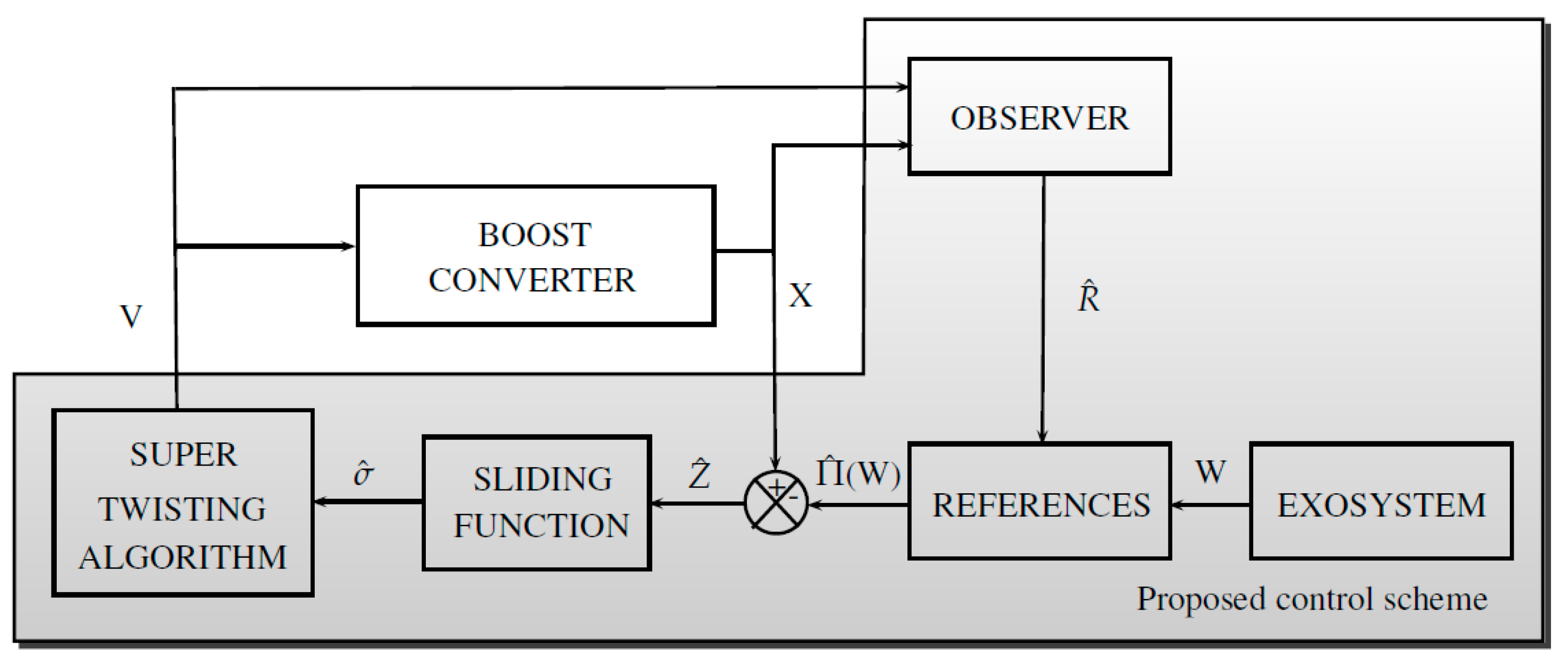
The proposed control scheme is illustrated in Figure 3. The EXOSYSTEM block (defined in Equation (4) or (10)) generates the sinusoidal and constant signals that are fed to the REFERENCES block. This block generates the ideal steady state in Equations (55) and (57) for the boost circuit. Then, this steady state is compared with the real state of the boost circuit, obtaining the error signal vector shown in Equation (7). From the elements of this vector, the sliding function in Equation (20) is constructed as a linear combination and used in a super-twisting algorithm (Equations (21) and (22)). This control action is fed to the boost circuit and to the observer in Equation (59), along with the real state. The observer generates an estimate for the load resistance that is used for updating the ideal steady state for finally closing the loop.
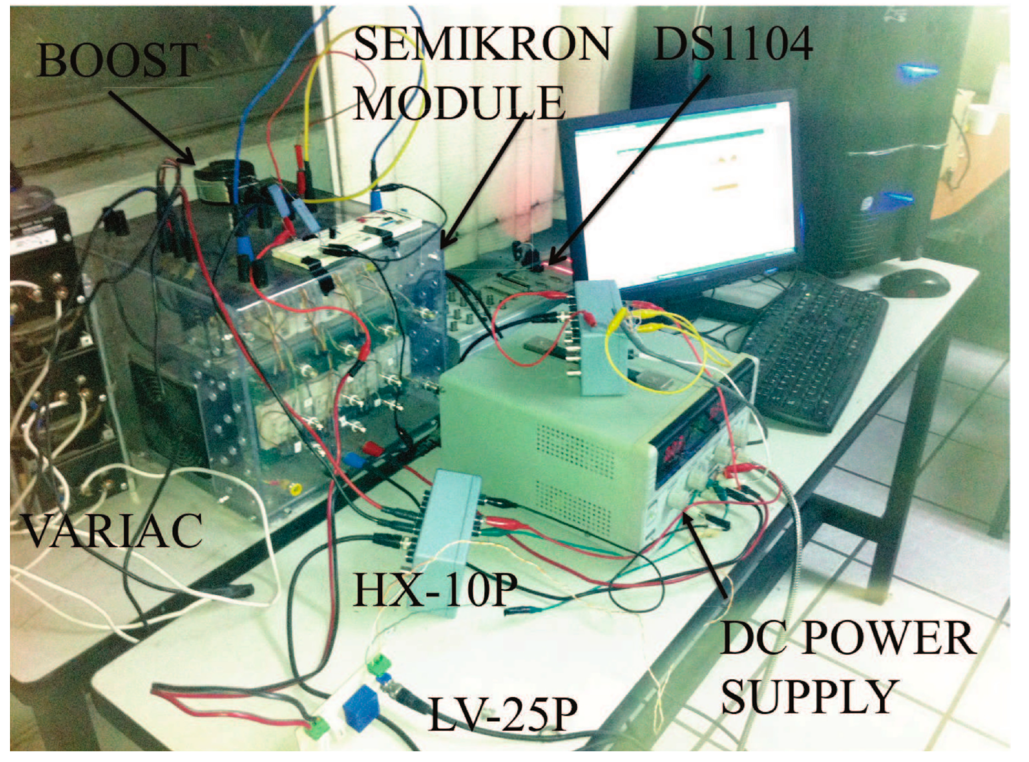
The proposed control scheme was implemented in a dSPACE 1104 board, represented by the gray shape; outside the board, a boost converter was connected using a Semikron module and controlled by the dSPACE board programmed with the control.
Figure 3 represents only the control signals.
The boost converter parameters used for the experimental results were L = 0.098 H, C = 10 mF, R = 200 Ω, and E = 8 V (actually, this value was considered to be 10 V in the control algorithm in order to introduce a perturbation for all time). The design parameter c1 was fixed to a value of −200, which corresponds to an eigenvalue λ1 = −412.2.
Remark 4.
In order for Equation (26) not to reach zero, c1 should not be selected as
c 1 = L ( z 1 + π 1 ) C ( z 2 + π 2 ) = L ( x 1 ) C ( x 2 ) .
Since x1 > 0 and x2 > 0, it is clear that c1 should at least not be positive in order to avoid δ(z,ω) = 0.
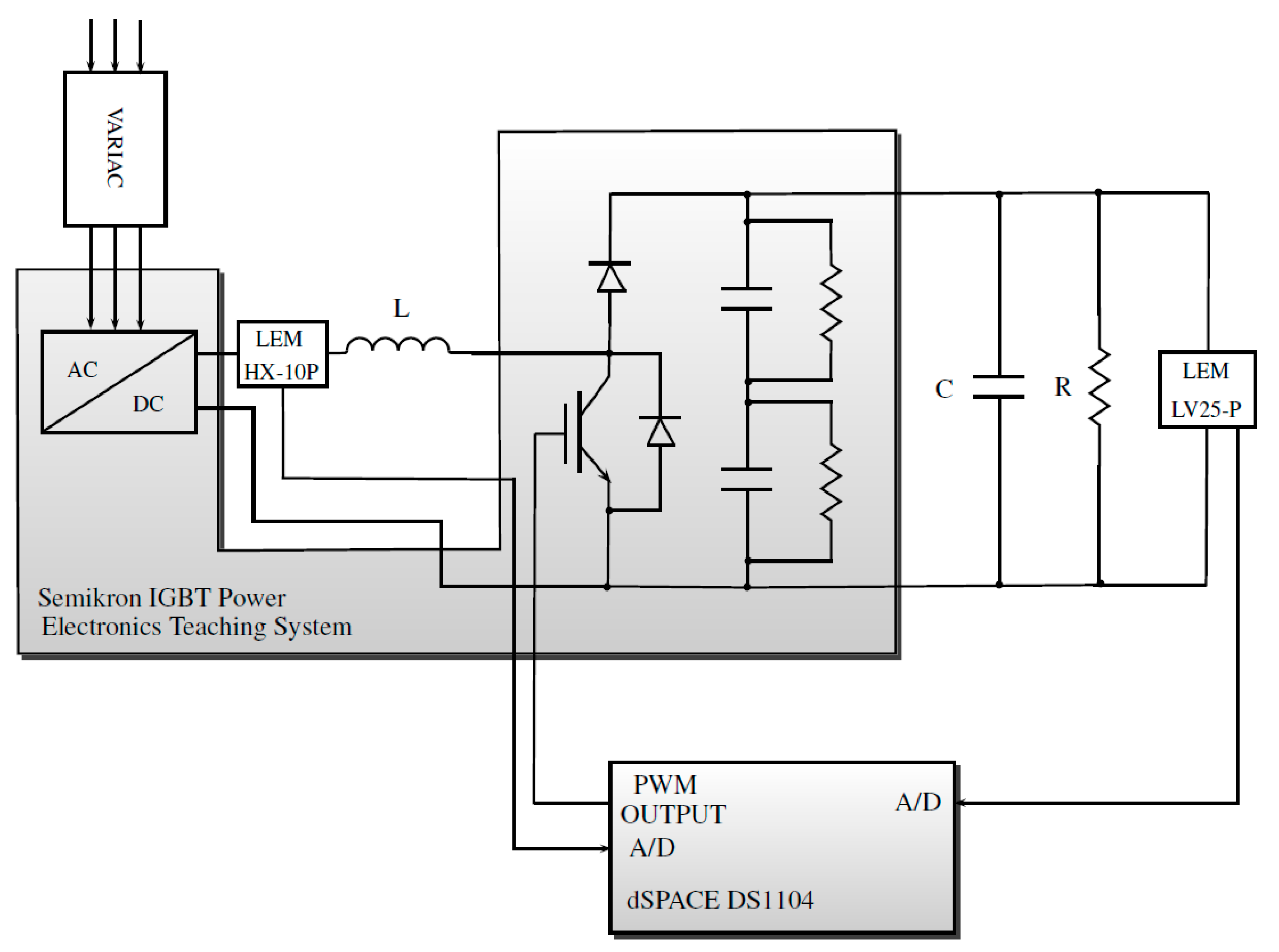
The input voltage source is made by a three-phase uncontrolled diode rectifier fed by a three-phase variable transformer (VARIAC). The input voltage can be adjusted by rotating the VARIAC knob. The resulting DC voltage is used to feed a Semikron power module. The Semikron power module is used to feed the boost converter. The controller is programmed in Simulink along with the PWM generator, and the output signals from Simulink are obtained with a dSPACE 1104 board. The board contains ADC converters to acquire the current through the inductor and the voltage across the capacitor. The used voltage and current sensors are the LEM HX 10-P and the LEM LV 25-P. Figure 4 shows a diagram of the experimental setup, and Figure 5 shows a photo of the prototype.
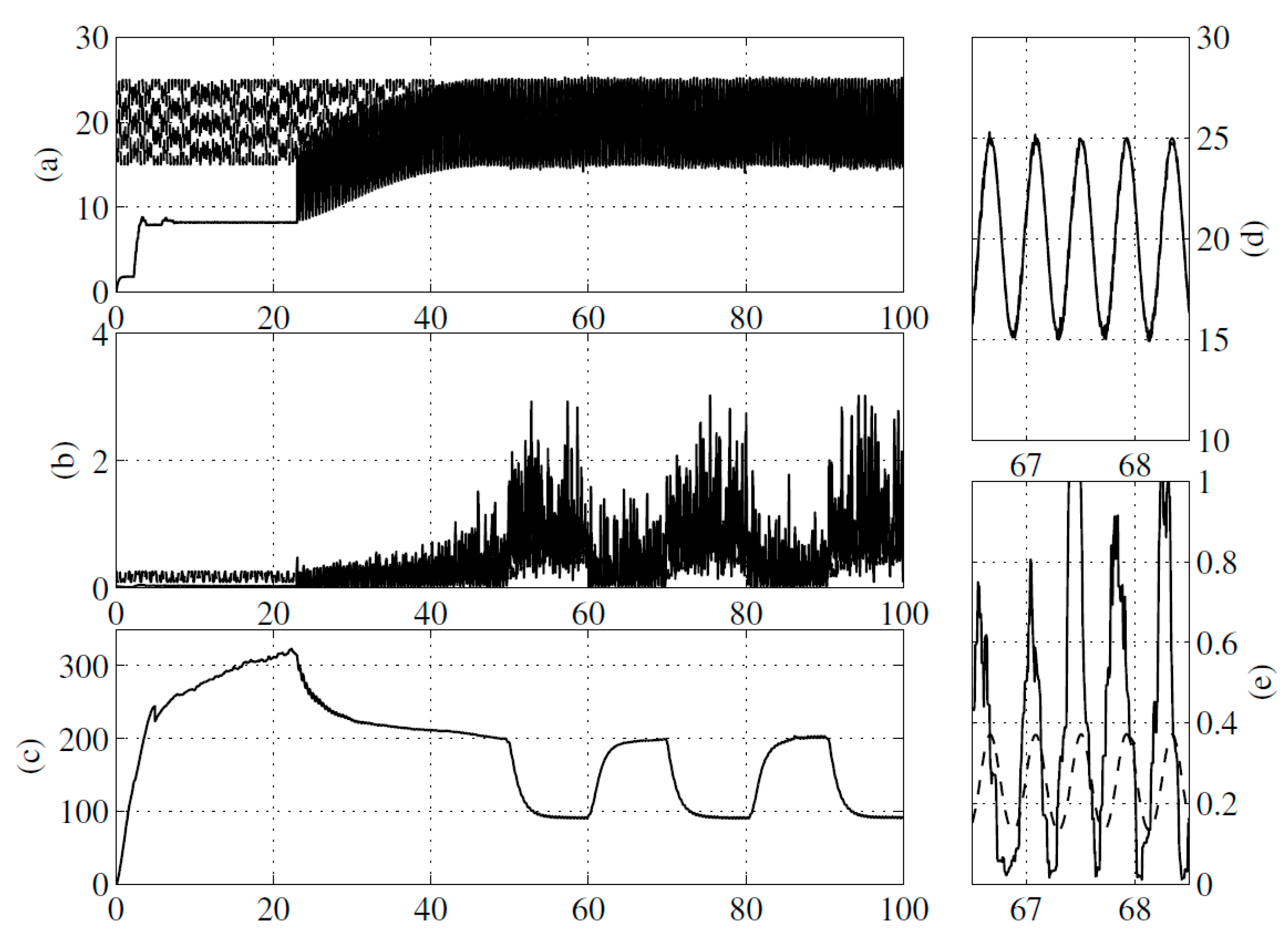
A first-order Butterworth low-pass filter having an edge frequency of 100 rad/s was used for filtering the inductor current in order to attenuate the measurement noise. The used sampling period was h = 60 ms. Initially, v was fixed at a value of 1 to operate the converter in an open-loop mode, where the output capacitor voltage was the same as the input voltage E, calibrated at a value of 8 V (actually this value was considered to be 10 V in the control algorithm in order to introduce a perturbation for all time). Then, the converter was operated in closed-loop mode, allowing the observation of transient responses. The load resistance variations were introduced as steps. At time instants 50, 70, and 90 s, the resistance was reduced to approximately 50% of its nominal value; at time instants 60 and 80 s, the load resistance recovered to its nominal value.
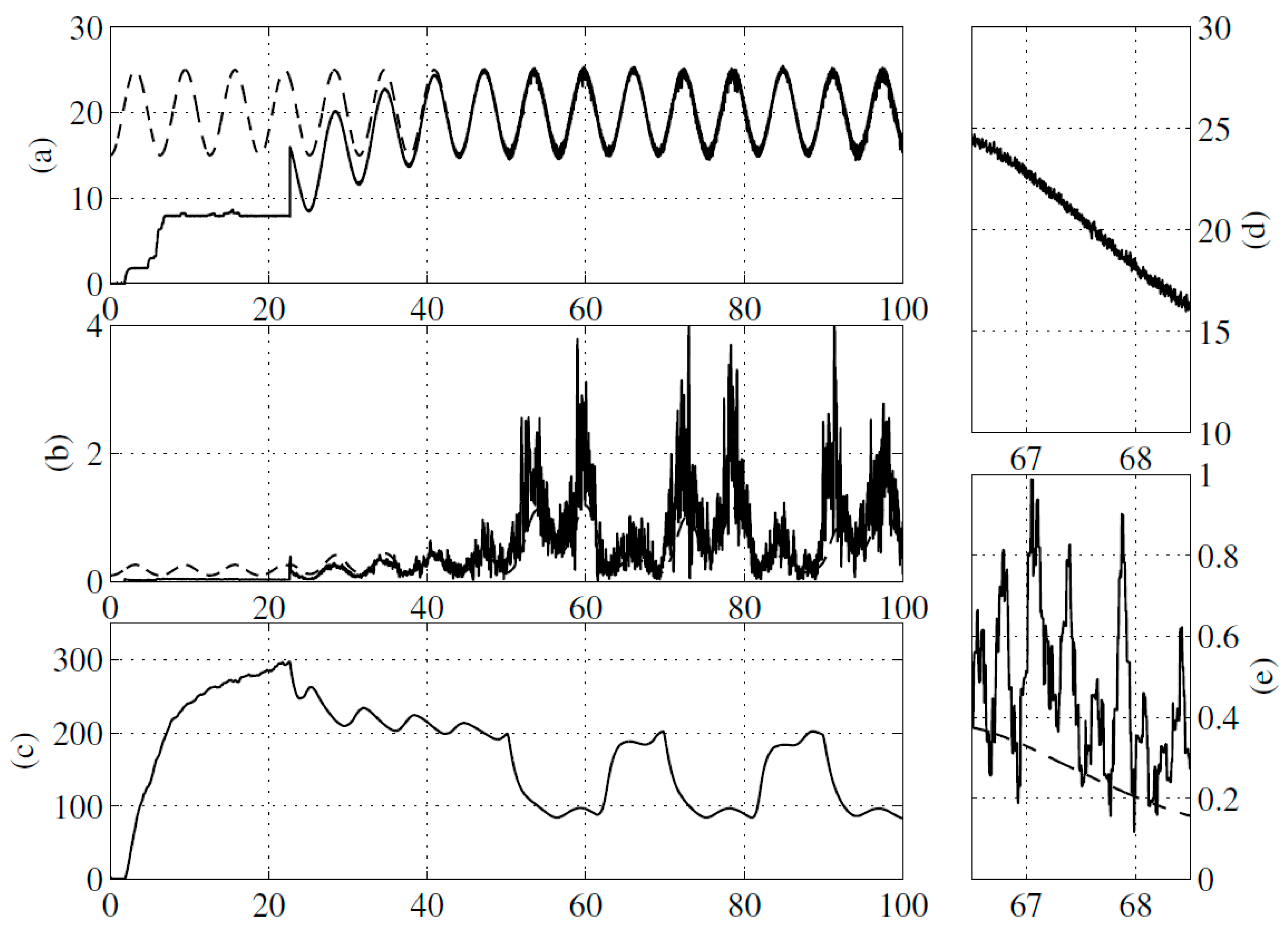
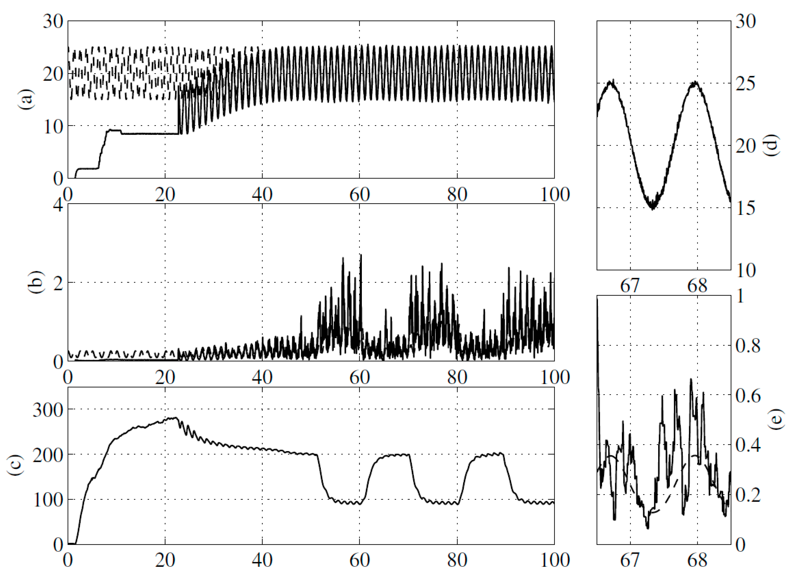
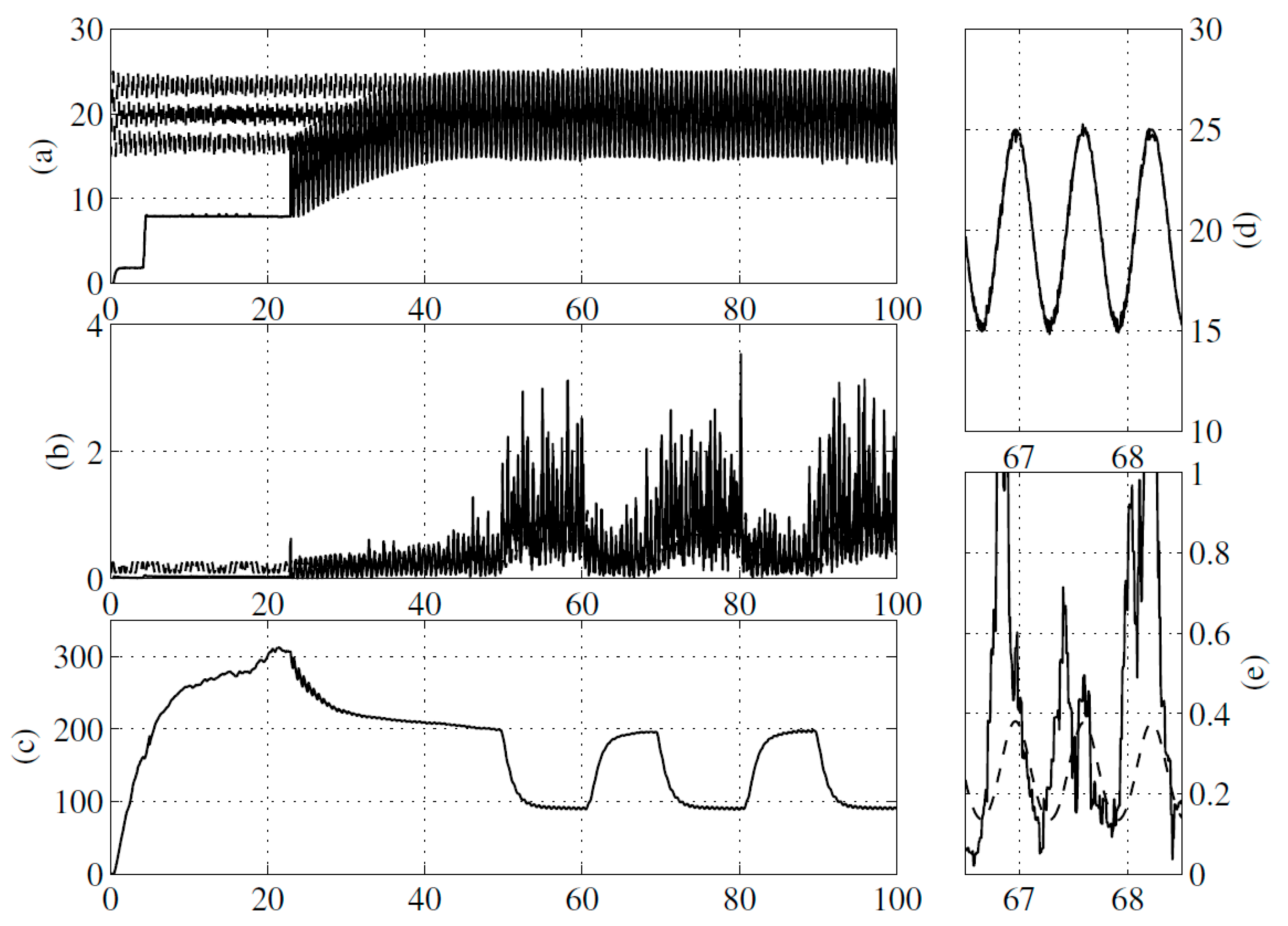
The capacitor voltage was forced to follow a signal with a sine waveform whose amplitude was equal to 5 V plus a DC (bias) voltage whose amplitude is 20 V. Several results were obtained with different frequency. Figure 6 shows the results for a frequency value of 1 rad/s, Figure 7 shows the results for a frequency of 5 rad/s, Figure 8 shows the results for a frequency of 10 rad/s, and Figure 9 shows the results for a frequency of 15 rad/s.
In general, a similar behavior can be appreciated in all cases, i e., a good performance for the voltage across the capacitor where the exponentially transient response (without overshoot) was due to the natural sliding mode dynamics in all cases, although the inductor current tracking was not clear due to measurement noise. It is important to mention that, in all cases, there were minimal transient responses at the voltage across the capacitor when load resistance variations were introduced. On the contrary, the transient responses of the output capacitor voltages reported in [34,35,36], through simulation studies, were considerably larger.
In order to better evaluate the control performance at all four frequencies, we considered the precision error Pe and the chattering effect Ch. The former is defined as the relative error of the output variable and is calculated as the difference between the average steady-state control output and the reference value, divided by the reference value:
P e = | S r V m c | S r × 100 ,
where Sr is the imposed reference, and Vmc is the average of the output controlled variable in the steady state. The latter is characterized by the amplitude of the signal, and is given by the difference between the amplitude of the output variable and the average in the steady state of the reference signal:
C h = | A m c V m c | V c m × 100 ,
where Amc is the maximum amplitude of the deviations of the output signal with respect to its average value Vmc.
Table 1 summarizes the evaluation parameters for all four frequencies. One can observe that the proposed controller had approximately a zero precision error at all frequencies, but the chattering effect decreased as the frequency increased. One final observation can be drawn between the inductor current and the load resistance. The current increased as the load resistance decreased and vice versa. This was expected since π1(w) was updated with the resistance estimation.

4. Conclusions

A second-order SM output regulation control technique was successfully applied to the DC-biased sinusoidal boost power conversion problem. The inductor current reference signal was proposed with a third-order polyonomy as an approximated solution for one of the Francis–Isidori–Byrnes equations with satisfactory accuracy. Additionally, the nonminimum phase dynamics at the inductor current were stabilized with a proper selection of the sliding function. Experimental results demonstrated the robust performance of the proposed control strategy in the presence of plant parameter variations, corroborating the merits of this technique.

Author Contributions

J.R. and S.O.-C. contributed to the conceptualization of the article; J.C.R.-C. and O.-F.R.-M. contributed to the methodology; J.R. contributed to the software and validation, J.R. and S.O.-C. contributed to the formal analysis; J.R., S.O.-C. and J.C.R.-C. wrote the draft and prepared the manuscript. All authors have read and agreed to the published version of the manuscript.

Funding

The authors would like to thank the CINVESTAV del IPN and the Universidad Panamericana.

Institutional Review Board Statement

Not applicable.

Informed Consent Statement

Not applicable.

Data Availability Statement

Not applicable.

Conflicts of Interest

The authors declare no conflict of interest.

Appendix A. Direct Control Method

The direct control method consists of directly controlling the output capacitor voltage. In the case of DC-to-DC conversion, the corresponding reference signals for the inductor current and output capacitor voltage are as follows [37]:
x 1 , r = V d 2 R E ,     x 2 , r = V d ,
where Vd > E. The tracking errors are defined as e1 = x1x1,r and e2 = x2x2,r, whose dynamics are
e ˙ 1 = e 2 + x 2 , r L v + E L ,
e ˙ 2 = e 1 + x 1 , r C v + e 2 + x 2 , r R C ,
where k2 < 0. This control action leads to e ˙ 2 = k2e2. In this case, the residual dynamics result in the following form:
e ˙ 1 = e 2 + x 2 , r L ( k 2 e 2 + e 2 R C + V d R E e 1 + x 1 , r ) + E L .
Linearizing around e1 = 0 yields
e ˙ 1 = R E C V d 2 e 1 + H . O . T . ,
where the unstable behavior of the zero dynamics can be appreciated.

Appendix B. Indirect Control Method

The indirect control method consists of controlling the inductor current. Using Equation (A2), control v is determined as follows:
v = ( k 1 e 1 E L ) L e 2 + x 2 , r ,
where k1 < 0. It is clear that the dynamic equation of e1 under the proposed control results in e ˙ 1 = k1e1. Then, the residual dynamics are expressed as
e ˙ 2 = e 1 + x 1 , r C ( ( k 1 e 1 E L ) L e 2 + x 2 , r ) e 2 + x 2 , r R C ,
The corresponding zero dynamics when e1 = 0 are of the following form:
e ˙ 2 = x 1 , r C ( E L ) L e 2 + x 2 , r e 2 + x 2 , r R C .
The linear approximation around e2 = 0 is expressed in the following form:
e ˙ 2 = ( 1 R C + 1 ) e 2 + H . O . T . ,
where the minimum phase behavior of the boost converter can be appreciated.

Appendix C. Determination of the Constants in Equations (20)–(22)

The controller stabilizes the boost converter when satisfying the following bound:
| c 1 E L c 1 π 1 ( ω ) ω S ω z 2 + π 2 ( ω ) R C π 2 ( ω ) ω S ω | η m .
For some constant ηm > 0. This can be achieved by noting that some terms on the left side in the above condition are known, where a maximal value, i.e.,
max { c 1 E L c 1 π 1 ( ω ) ω S ω π 2 ( ω ) ω S ω } ,
can easily be determined, and by considering that the initial state x2(0) = z2(0) + π2(w)(0). Once these conditions are verified, the controller gains are selected to satisfy
k 2 > η m ,
k 1 4 η m ( k 2 + η m ) ( k 2 η m ) .
Then, the sliding variable σ(t) converges to zero in finite time tS [33].

References

  1. Rashid, M. Power Electronics: Circuits, Devices and Applications, 3rd ed.; Prentice Hall: London, UK, 2004; p. 762. [Google Scholar]
  2. Undeland, M.N.; Robbins, W.P.; Mohan, N. Power Electronics. In Converters, Applications, and Design, 3rd ed.; John Whiley & Sons: Hoboken, NJ, USA, 1995; p. 763. [Google Scholar]
  3. Erickson, R.W.; Maksimovic, D. Fundamentals of Power Electronics; Springer: New York, NY, USA, 2001. [Google Scholar]
  4. Caceres, R.O.; Barbi, I. A boost DC-AC converter: Analysis, design, and experimentation. IEEE Trans. Power Electron. 1999, 14, 134–141. [Google Scholar] [CrossRef]
  5. Jang, M.; Agelidis, V.G. A Minimum Power-Processing-Stage Fuel-Cell Energy System Based on a Boost-Inverter with a Bidirectional Backup Battery Storage. IEEE Trans. Power Electron. 2010, 26, 1568–1577. [Google Scholar] [CrossRef]
  6. Jha, K.; Mishra, S.; Joshi, A. High-Quality Sine Wave Generation Using a Differential Boost Inverter at Higher Operating Frequency. IEEE Trans. Ind. Appl. 2015, 51, 373–384. [Google Scholar] [CrossRef]
  7. Tang, Y.; Bai, Y.; Kan, J.; Xu, F. Improved Dual Boost Inverter with Half Cycle Modulation. IEEE Trans. Power Electron. 2017, 32, 7543–7552. [Google Scholar] [CrossRef]
  8. Wickramasinghe Abeywardana, D.B.; Acuna, P.; Hredzak, B.; Aguilera, R.P.; Agelidis, V.G. Single-Phase Boost Inverter-Based Electric Vehicle Charger with Integrated Vehicle to Grid Reactive Power Compensation. IEEE Trans. Power Electron. 2018, 33, 3462–3471. [Google Scholar] [CrossRef]
  9. Khan, A.A.; Lu, Y.W.; Eberle, W.; Wang, L.; Khan, U.A.; Cha, H. Single-Phase Split-Inductor Differential Boost Inverters. IEEE Trans. Power Electron. 2020, 35, 107–120. [Google Scholar] [CrossRef]
  10. Zhao, W.; Lu, D.D.-C.; Agelidis, V.G. Current Control of Grid-Connected Boost Inverter with Zero Steady-State Error. IEEE Trans. Power Electron. 2011, 26, 2825–2834. [Google Scholar] [CrossRef]
  11. Wai, R.-J.; Lin, Y.-F.; Liu, Y.-K. Design of Adaptive Fuzzy-Neural-Network Control for a Single-Stage Boost Inverter. IEEE Trans. Power Electron. 2015, 30, 7282–7298. [Google Scholar] [CrossRef]
  12. Zhu, G.-R.; Xiao, C.-Y.; Wang, H.-R.; Tan, S.-C. Closed-loop waveform control of boost inverter. IET Power Electron. 2016, 9, 1808–1818. [Google Scholar] [CrossRef]
  13. Abeywardana, D.B.W.; Hredzak, B.; Agelidis, V.G. An Input Current Feedback Method to Mitigate the DC-Side Low-Frequency Ripple Current in a Single-Phase Boost Inverter. IEEE Trans. Power Electron. 2016, 31, 4594–4603. [Google Scholar] [CrossRef]
  14. Abeywardana, D.B.W.; Hredzak, B.; Agelidis, V.G. A Rule-Based Controller to Mitigate DC-Side Second-Order Harmonic Current in a Single-Phase Boost Inverter. IEEE Trans. Power Electron. 2016, 31, 1665–1679. [Google Scholar] [CrossRef]
  15. Huang, S.; Tang, F.; Xin, Z.; Xiao, Q.; Loh, P.C. Grid-Current Control of a Differential Boost Inverter with Hidden LCL Filters. IEEE Trans. Power Electron. 2019, 34, 889–903. [Google Scholar] [CrossRef]
  16. El Aroudi, A.; Haroun, R.; Al-Numay, M.; Huang, M. Multiple-Loop Control Design for a Single-Stage PV-Fed Grid-Tied Differential Boost Inverter. Appl. Sci. 2020, 10, 4808. [Google Scholar] [CrossRef]
  17. Rasheduzzaman, M.; Fajri, P.; Kimball, J.; Deken, B. Modeling, Analysis, and Control Design of a Single-Stage Boost Inverter. Energies 2021, 14, 4098. [Google Scholar] [CrossRef]
  18. Liu, B.; He, D.; Li, G.; Liu, H.; Yang, L.; Chen, Y. Single-Loop Control for Single-Phase Dual-Boost Grid-Tied Inverter with Half Cycle Modulation and Feedforward Virtual-Vectors MPC. IEEE Trans. Ind. Electron. 2022, 69, 13918–13924. [Google Scholar] [CrossRef]
  19. Lopez-Caiza, D.; Renaudineau, H.; Muller, N.; Flores-Bahamonde, F.; Kouro, S.; Rodriguez, J. Dual-Boost Inverter for PV Microinverter Application—An Assessment of Control Strategies. Appl. Sci. 2022, 12, 5952. [Google Scholar] [CrossRef]
  20. Cavallo, A.; Russo, A.; Canciello, G. Hierarchical control for generator and battery in the more electric aircraft. Sci. China Inf. Sci. 2019, 62, 192207. [Google Scholar] [CrossRef]
  21. Russo, A.; Canciello, G.; Cavallo, A. Generalized Super-Twisting control of a Dual Active Bridge for More Electric Aircraft. In Proceedings of the 2021 European Control Conference (ECC), Delft, The Netherlands, 29 June–2 July 2021; pp. 1610–1615. [Google Scholar]
  22. Cortes, D.; Vazquez, N.; Alvarez-Gallegos, J. Dynamical Sliding-Mode Control of the Boost Inverter. IEEE Trans. Ind. Electron. 2009, 56, 3467–3476. [Google Scholar] [CrossRef]
  23. Flores-Bahamonde, F.; Valderrama-Blavi, H.; Bosque, J.M.; García, G.; Martinez-Salamero, L. Using the sliding-mode control approach for analysis and design of the boost inverter. IET Power Electron. 2016, 9, 1625–1634. [Google Scholar] [CrossRef]
  24. Wickramasinghe Abeywardana, D.B.; Hredzak, B.; Agelidis, V.G. A Fixed-Frequency Sliding Mode Controller for a Boost-Inverter-Based Battery-Supercapacitor Hybrid Energy Storage System. IEEE Trans. Power Electron. 2017, 32, 668–680. [Google Scholar] [CrossRef]
  25. Lopez-Caiza, D.; Flores-Bahamonde, F.; Kouro, S.; Santana, V.; Müller, N.; Chub, A. Sliding Mode Based Control of Dual Boost Inverter for Grid Connection. Energies 2019, 12, 4241. [Google Scholar] [CrossRef]
  26. López-Santos, O.; García, G. Double Sliding-Surface Multiloop Control Reducing Semiconductor Voltage Stress on the Boost Inverter. Appl. Sci. 2020, 10, 4912. [Google Scholar] [CrossRef]
  27. Sira-Ramírez, H. DC-to-AC power conversion on a ‘boost’converter. Int. J. Robust Nonlinear Control 2001, 11, 589–600. [Google Scholar] [CrossRef]
  28. Phogat, K.S.; Chang, D.E. Model Predictive Regulation on Manifolds in Euclidean Space. Sensors 2022, 22, 5170. [Google Scholar] [CrossRef] [PubMed]
  29. Singh, S.K.; Singh, R.; Ashfaq, H.; Sharma, S.K.; Sharma, G.; Bokoro, P.N. Super-Twisting Algorithm-Based Virtual Synchronous Generator in Inverter Interfaced Distributed Generation (IIDG). Energies 2022, 15, 5890. [Google Scholar] [CrossRef]
  30. Ramos, L.; Castillo-Toledo, B.; Alvarez, J. Nonlinear regulation of an underactuated system. In Proceedings of the IEEE International Conference on Robotics and Automation, Albuquerque, NM, USA, 20–25 April 1997; Volume 4, pp. 3288–3293. [Google Scholar]
  31. Sanposh, P.; Tarn, T.; Cheng, D. Theory and experimental results on output regulation for nonlinear systems. In Proceedings of the American Control Conference, Anchorage, AK, USA, 8–10 May 2002; Volume 1, pp. 96–101. [Google Scholar]
  32. Rivera, J.; Loukianov, A.; Castillo-Toledo, B. Discontinuous output regulation of the Pendubot. In Proceedings of the 17th World Congress of the International Federation of Automatic Control, Seoul, Republic of Korea, 6–11 July 2008. [Google Scholar]
  33. Levant, A. Sliding order and sliding accuracy in sliding mode control. Int. J. Control 1993, 58, 1247–1263. [Google Scholar] [CrossRef]
  34. Shtessel, Y.B.; Zinober, A.S.; Shkolnikov, I.A. Sliding mode control of boost and buck-boost power converters using method of stable system centre. Automatica 2003, 39, 1061–1067. [Google Scholar] [CrossRef]
  35. Olm, J.; Ros, X.; Shtessel, Y. Stable inversion-based robust tracking control in DC-DC nonlinear switched converters. In Proceedings of the Decision and Control (CDC) Held Jointly with the 2009 28th Chinese Control Conference (CCC), Shanghai, China, 15–18 December 2009; pp. 2789–2794. [Google Scholar]
  36. Olm, J.; Ros, X. Approximate tracking of periodic references in a class of bilinear systems via stable inversion. Discret. Contin. Dyn. Syst. Ser. B 2011, 15, 197–215. [Google Scholar]
  37. Utkin, V.; Guldner, J.; Shi, J. Sliding Mode Control in Electromechanical Systems; Taylor & Francis: Philadelphia, PA, USA, 1999. [Google Scholar]
Figure 1. (a) A boost inverter; (b) equivalent circuit with voltage sources; (c) voltage signals constituting the output voltage.
Applsci 13 05963 g001
Figure 2. Boost converter circuit.
Applsci 13 05963 g002
Figure 3. Proposed control scheme block diagram.
Applsci 13 05963 g003
Figure 4. Experimental setup schematic diagram, including the proposed control scheme.
Applsci 13 05963 g004
Figure 5. Photograph of the prototype.
Applsci 13 05963 g005
Figure 6. Real-time results at α = 1 rad/s. (a) Capacitor voltage (solid) and capacitor voltage reference signal (dashed) [V vs. s]. (b) Inductor current (solid) and inductor current reference signal (dashed) [A vs. s]. (c) Estimated load resistance [Ω vs. s]. (d) Zoomed-in view of the same variables in (a). (e) Zoomed-in view of the same variables in (b).
Applsci 13 05963 g006
Figure 7. Real-time results with α = 5 rad/s. (a) Capacitor voltage (solid) and capacitor voltage reference signal (dashed) [V vs. s]. (b) Inductor current (solid) and inductor current reference signal (dashed) [A vs. s]. (c) Estimated load resistance [Ω vs. s]. (d) Zoomed-in view of the same variables in (a). (e) Zoomed-in view of the same variables in (b).
Applsci 13 05963 g007
Figure 8. Real-time results with α = 10 rad/s. (a) Capacitor voltage (solid) and capacitor voltage reference signal (dashed) [V vs. s]. (b) Inductor current (solid) and inductor current reference signal (dashed) [A vs. s]. (c) Estimated load resistance [Ω vs. s]. (d) Zoomed-in view of the same variables in (a). (e) Zoomed-in view of the same variables in (b).
Applsci 13 05963 g008
Figure 9. Real-time results with α = 15 rad/s. (a) Capacitor voltage (solid) and capacitor voltage reference signal (dashed) [V vs. s]. (b) Inductor current (solid) and inductor current reference signal (dashed) [A vs. s]. (c) Estimated load resistance [Ω vs. s]. (d) Zoomed-in view of the same variables in (a). (e) Zoomed-in view of the same variables in (b).
Applsci 13 05963 g009
Table 1. Evaluation Parameters for all four frequencies.
FrequencyPeCh
1 rad/s≈0%2.2%
5 rad/s≈0%1.31%
10 rad/s≈0%1.09%
15 rad/s≈0%0.44%
Disclaimer/Publisher’s Note: The statements, opinions and data contained in all publications are solely those of the individual author(s) and contributor(s) and not of MDPI and/or the editor(s). MDPI and/or the editor(s) disclaim responsibility for any injury to people or property resulting from any ideas, methods, instructions or products referred to in the content.

