Article

M-ary Amplitude Shift Keying Power and Information Synchronous Transmission Based on Phase-Shifted Full-Bridge

1
Tianjin Key Laboratory of Electrical Equipment Intelligent Control, Tiangong University, Tianjin 300384, China
2
State Key Laboratory of Reliability and Intelligence of Electrical Equipment, Hebei University of Technology, Tianjin 300401, China
*
Author to whom correspondence should be addressed.
Appl. Sci. 2023, 13(1), 475; https://doi.org/10.3390/app13010475
Submission received: 26 November 2022 / Revised: 23 December 2022 / Accepted: 27 December 2022 / Published: 29 December 2022

Abstract

:
This paper proposes an M-ary amplitude shift keying (MASK) power and information synchronous transmission system based on phase-shifted full-bridge (PSFB) for applications in wireless power transmission (WPT). The Pulse Width Modulation (PWM) waveform uses different phases to control the MOSFET in the full-bridge inverter for MASK modulation. The inverter voltage generates M amplitude transformation, forming a comprehensive power information flow. The demodulation circuit processes the information transmitted to the secondary side, following the power supply with a differential amplifier, to realize synchronous transmission of power supply and information. Compared with conventional amplitude modulation, the system’s volume is significantly reduced, and the DC-DC modulation circuit has no filtering effect. It transmits comprehensive high-level data and improves the information transmission rate from the perspective of bit width. In the experiment, 16-bit width data are transmitted, and the bit rate is increased by four times compared to conventional amplitude modulation. Combined with DSP, the designed demodulation circuit reduces the voltage amplitude fluctuation at the receiving end to 5% and minimizes the impact of amplitude modulation voltage fluctuation on the system.

1. Introduction

The application of wireless power transmission (WPT) technology [1,2,3] is more and more extensive. Compared with the conventional wired charging method, it avoids the wear of the joint during the charging of the equipment, as well as the sparks and other safety hazards generated during the insertion and extraction process. It is safe, reliable, flexible and convenient. WPT covers many fields [4,5] such as medicine [6], industry and electric vehicles, but in most application scenarios, higher requirements are proposed for the performance of wireless transmission systems, such as real-time control, signal transmission, etc. It requires the system to achieve information interaction while performing wireless power transmission; that is, power and information synchronous transmission technology [7,8].
At present, the power and information synchronous transmission technology of a wireless power transmission system can be divided into three types: ratio frequency technologies [9,10], dual channel transmission technology [11,12] and single-channel transmission technology [13,14]. The ratio frequency technology is a communication method which uses electromagnetic wave to realize the information transmission and exchange. With the development of radio frequency communication technology, it has been integrated into every corner of production and life, such as RFID, BlueTooth, Wi-Fi, Zigbee [15] and so on. However, it also has many problems, such as the long duration of a ‘handshake’ in communication and the limitation of application field. The dual-channel transmission technology is used to establish an additional channel based on the original power transmission channel. Reference [16] used dual-channel transmission technology, through low-frequency transmission power and high-frequency transmission of information, used in the medical field to achieve simultaneous transmission. Its data transmission rate is fast, but its structure is complex, and there is interference between signal and power, which makes the bit error rate high. Compared with the dual-channel technology, the single-channel transmission technology indicates that the power and the information share a transmission channel. The system structure is simple and avoids the cross coupling between the two channels in the dual channel transmission technology. It has become a hotspot in the research of simultaneous communication. Single-channel transmission technology can be divided into carrier modulation [17] and power modulation. In Reference [18], a double-sided LCC compensation topology for power transmission is adopted, and the data transmission channel is composed of a four-resonance dual-rejection structure used to realize synchronous transmission of power and information. There are many methods of power modulation. Reference [19] realized the synchronous transmission of power and signal by controlling the phase of current and voltage. Reference [20] used the baseband signal to change the magnitude of the input voltage amplitude for signal transmission, which is a traditional amplitude modulation method. This method not only solves the problem of power and information interference, but also reduces the bit error rate. However, the information transmission rate is low, and the output voltage is susceptible to fluctuations. At the same time, the addition of DC-DC modulation circuit makes the system structure more complex, and the system baud rate is affected.
The existing phase-shift modulation power and information simultaneous transmission methods [21,22] transmit power through the fundamental wave, changing the third harmonic amplitude to transmit information, and achieve power and information simultaneous transmission. The application of the phase-shifted full-bridge (PSFB) [23,24,25] means the system no longer needs to be controlled by an external modulation circuit, and the switch tube can achieve zero voltage switching (ZVS). The above power and information transmission technologies can only transmit two-bit signals: ‘0’and ‘1’. Reference [26] proposed a dual modulation strategy of power and data, which was applied to the DC-DC power converter to achieve ‘talkative power’. The frequency-hopping differential phase shift keying (FH-DPSK) modulation strategy is used to overcome the crosstalk between the selected transmission systems, and the transmission of ‘0’, ‘1’, ‘2’ and ‘3’ four-bit signals can be realized. However, this method uses cables or lights for information transmission, so the application field is limited.
The motivation of this work is to solve the problems of low information transmission rate and output voltage fluctuation in power modulation. A M-ary amplitude shift keying (MASK) power and information synchronous transmission system based on PSFB is proposed. The PWM variable generated by the pre-transmission modulation signal is directly superimposed on the control end of the MOSEFT in the full-bridge inverter to control the phase shift angle of the inverter, thereby changing the voltage amplitude and generating M amplitude transformations. The power and information are transmitted to the receiving coil at the same time through the transmitting coil, the power is transmitted to the load through the circuit, and the information is restored by the demodulation circuit and DSP.
The salient aspects of this paper are that the proposed method reduces the system’s volume without a DC-DC modulation circuit, reducing the influence of passive devices on the system and improving the baud rate of the system. At the same time, it transmits data with higher bit width, as 8-ary and 16-ary data, thereby increasing the information transmission rate to four times. The MASK modulation is adopted, and the electric power does not interfere with the signal. The designed demodulation circuit is combined with DSP to control the voltage amplitude fluctuation at the receiving end at 5% to minimize the influence of fluctuation on the load. Section 2 analyzes the system topology and mathematical model. In Section 3, the information modulation and demodulation methods are proposed, and the problems of power transmission efficiency and power, information transmission rate, and interference between information and power are analyzed. Section 4 verifies the feasibility of the method through experiments and simulations. Section 5 concludes the paper.

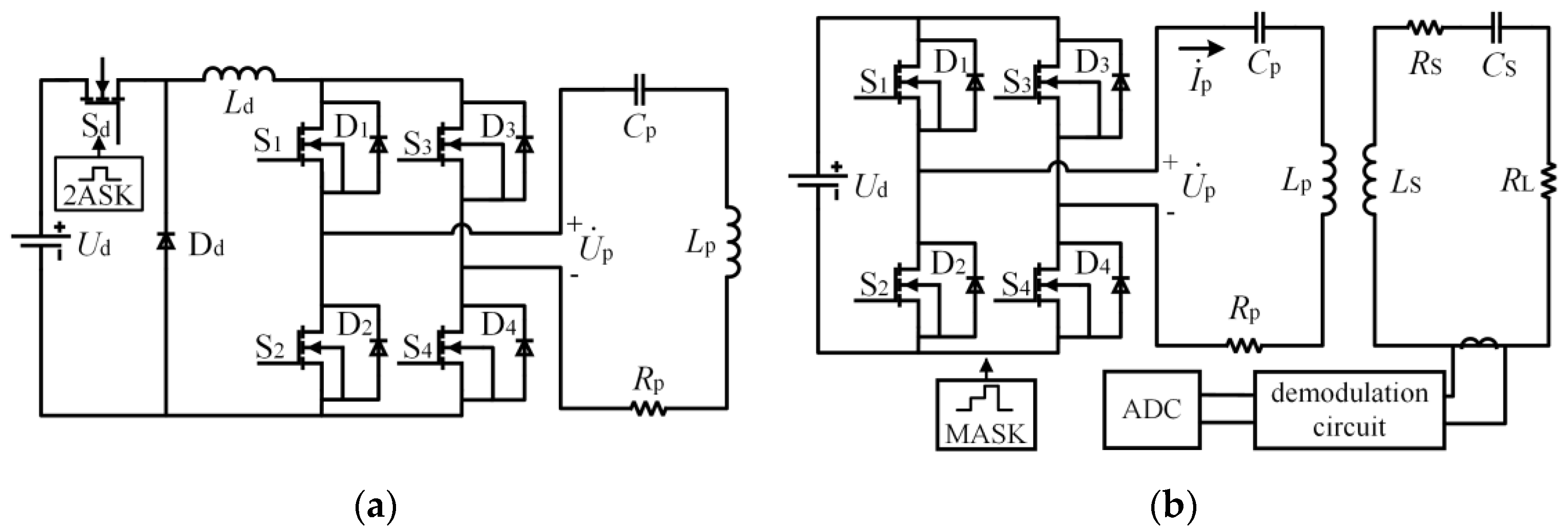
2. Structure and Modeling of the Proposed System

2.1. Structure of the Proposed System

The transmission circuit structure of the traditional amplitude modulated signal and power synchronous transmission system is shown in Figure 1a. The DC-DC modulation circuit is composed of a voltage source, a switch tube Sd, a diode Dd and an inductor Ld. MOSFET S1–S4 (S1 and S2 are leading leg, S3 and S4 are lagging leg) and diode D1–D4 form a full-bridge inverter circuit. The primary transmitting circuit and the secondary receiving circuit are consistent with Figure 1b. The DC-DC circuit Ld has the function of filtering, limiting the signal transmission baud rate and bit width. The structure of MASK modulated power and information synchronous transmission system based on PSFB is shown in Figure 1b. The DC-DC modulation circuit is removed, which makes the whole system structure simpler. At the same time, the influence of passive devices on the system is reduced, and the baud rate is improved. Without Ld filtering, higher bit width data can be transmitted. The transmitting circuit consists of transmitting coil Lp, its parasitic resistance Rp and compensating capacitance Cp. The receiving circuit includes a power-receiving part and an information-detecting part. LS, RS and CS are the inductance, internal resistance and compensation capacitance of the receiving coil of the power-receiving part. The information detection part demodulates the signal with DSP through demodulation circuit.
The output waveform of the full-bridge inverter during normal operation is shown in Figure 2. The DSP generates four pulse width modulation signals (US1US4) for MOSFET drive signals. The dotted lines are US4 and US3, and α is the phase shift angle. Up is the output voltage waveform of the full bridge inverter. Ip is the primary current waveform.
The time domain expression of inverter output voltage Up is:
U p ( φ ) { U d , φ ( 0 , π α ] 0 , φ ( π α , π ] U d , φ ( π , 2 π α ] 0 , φ ( 2 π α , 2 π ] ,
where Ud is the DC voltage source voltage. The Fourier series expansion of Equation (1) can be obtained:
U p ( φ ) = k = 1 4 U d k π cos ( k α 2 ) sin ( k α + k α 2 ) .
Therefore, the kth harmonic effective value of the inverter output voltage is:
U pk = 2 2 k π U i n | cos k α 2 | , k = 1 , 3 , 5   .
From Equation (3), it can be seen that when the input voltage is constant, the output voltage can only consider the fundamental wave due to the addition of the resonant compensation capacitor Cp at the transmitter. As the phase shift angle increases, the output fundamental component will continue to decrease to zero. By controlling the phase shift angle between the leading leg and the lagging leg of the PSFB, the effective value of the inverter voltage output by the system is changed. The electric power is transmitted to the receiving coil through the transmitting coil, so as to adjust the power coupled to the receiving coil and make the receiving voltage change linearly with the phase shift angle. The changing voltage amplitude corresponds to the transmission information, forming a comprehensive power information flow, realizing MASK modulation, and achieving the purpose of simultaneous transmission.

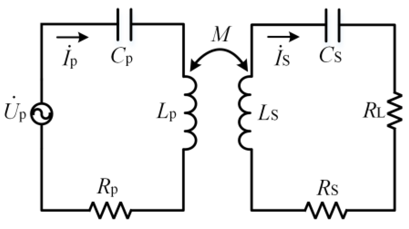
2.2. Equivalent Model Analysis of the System

The equivalent circuit of the system is shown in Figure 3. Up is the output voltage of the inverter and RL is the load. Ip and IS are the current on the emitting side and the receiving side, respectively. Lp and LS are the inductances of the transmitting coil and the receiving coil, respectively. Rp and RS are the internal resistance of the transmitting coil and the receiving coil, respectively. Cp and CS are the resonant capacitors of the transmitting side and the receiving side, respectively.
The circuit equivalent total impedance Zp and the receiver total impedance ZS can be expressed as:
{ Z s = j ω L s + 1 j ω C s + R L + R s Z p = j ω L p + 1 j ω C p + R p + ω 2 M 2 Z s .
In Equation (4), ω is the operating frequency of the system, and M is the mutual inductance between the transceiver coils. The current at the transmitter and receiver can be expressed as:
{ I ˙ p = U ˙ p Z p I ˙ s = I ˙ p     j ω M Z s .
The output power can be expressed as:
P out = | I ˙ s 2 R L | = 8 U in 2 ω 2 M 2 R L π 2 Z p 2 Z s 2 cos 2 α 2 ,
and the output efficiency can be expressed as:
η = P out P in = | I ˙ s 2 R L I ˙ p 2 Z p | = ω 2 M 2 R L Z s 2 Z p .
It can be seen from Equations (6) and (7) that the transmission power of the system is affected when the phase shift angle is changed, but the transmission efficiency of the system will not be affected. Therefore, during the simultaneous transmission of power and information, the output power fluctuation should be minimized while ensuring the transmission rate and controlling the bit error rate.

3. Synchronous Information Transmission Analysis

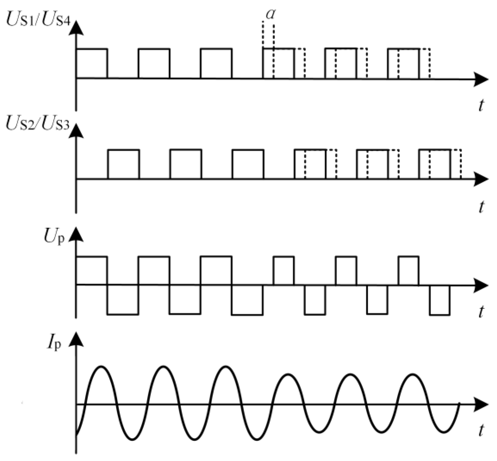
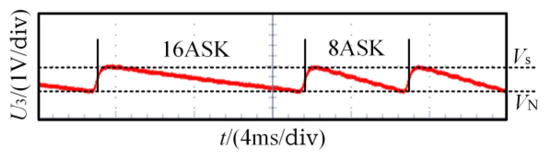
3.1. Information Modulation

As the phase shift angle changes, the inverter output voltage is shown in Figure 4, and the working and resonant frequency of the system is 47.3 kHz. This is consistent with the phenomenon of Figure 2; changing the phase shift angle to change the inverter voltage verified the feasibility of MASK modulation based on PSFB.
When ZS, Zp, ω, RL remain unchanged and the coupling coefficient k = 0.2, the change trend of the phase shift angle with output voltage and output power is shown in Figure 5. Experimental and simulation data reference Table 1.
Considering the voltage fluctuation problem, the voltage variation range is selected as 5%, and the corresponding α is 0–36.5°. Using DSP to generate PWM waves with different phases, 8ASK, 16ASK or higher MASK information modulation is performed to increase the signal bit width, thereby increasing the signal transmission rate. In the specified α range, according to Figure 5, the appropriate signal bit width, phase angle and corresponding voltage change value are selected. This can ensure the rate while reducing the bit error rate as much as possible. Table 2 shows the modulation parameters of 8-ary and 16-ary signal.

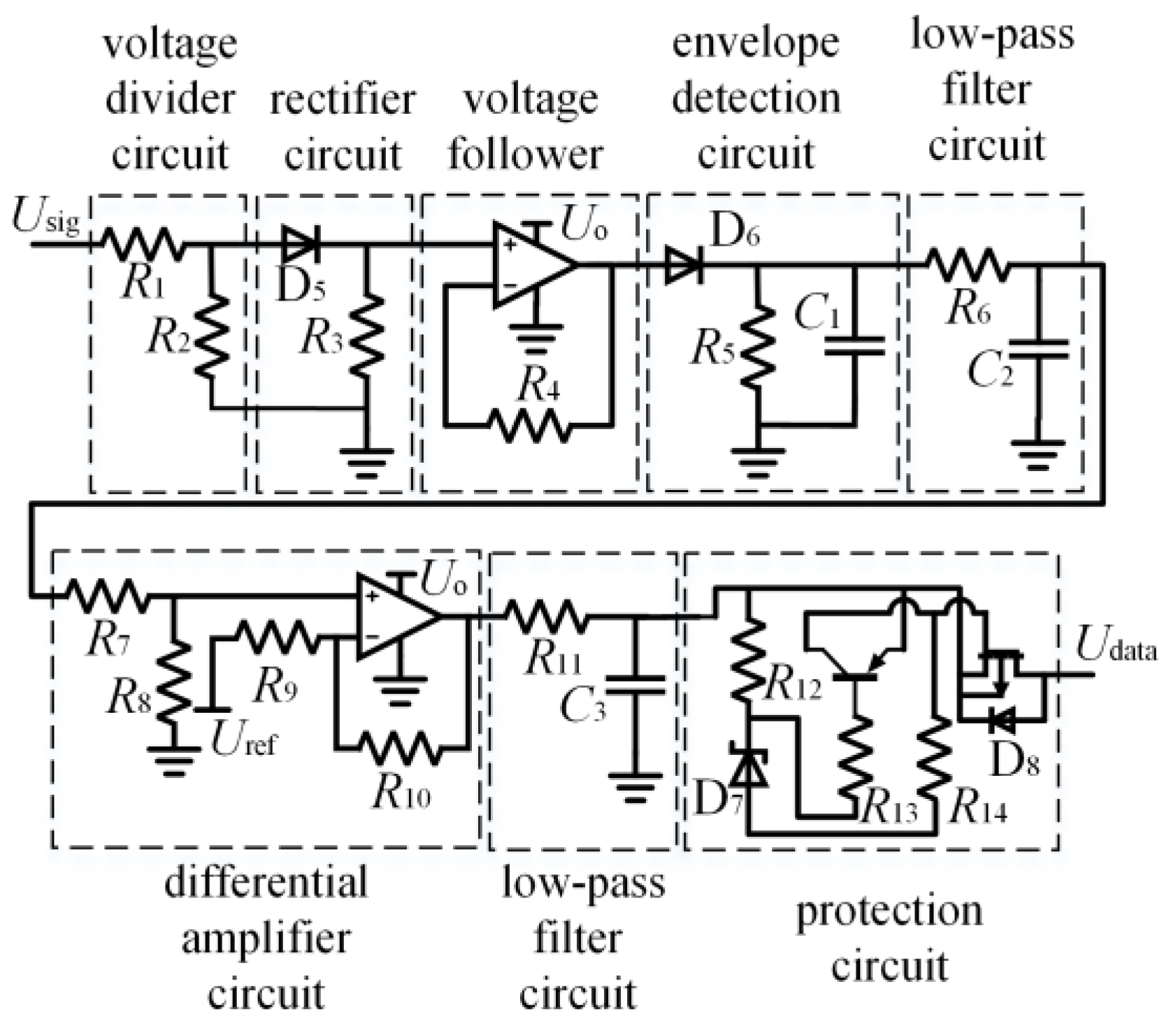
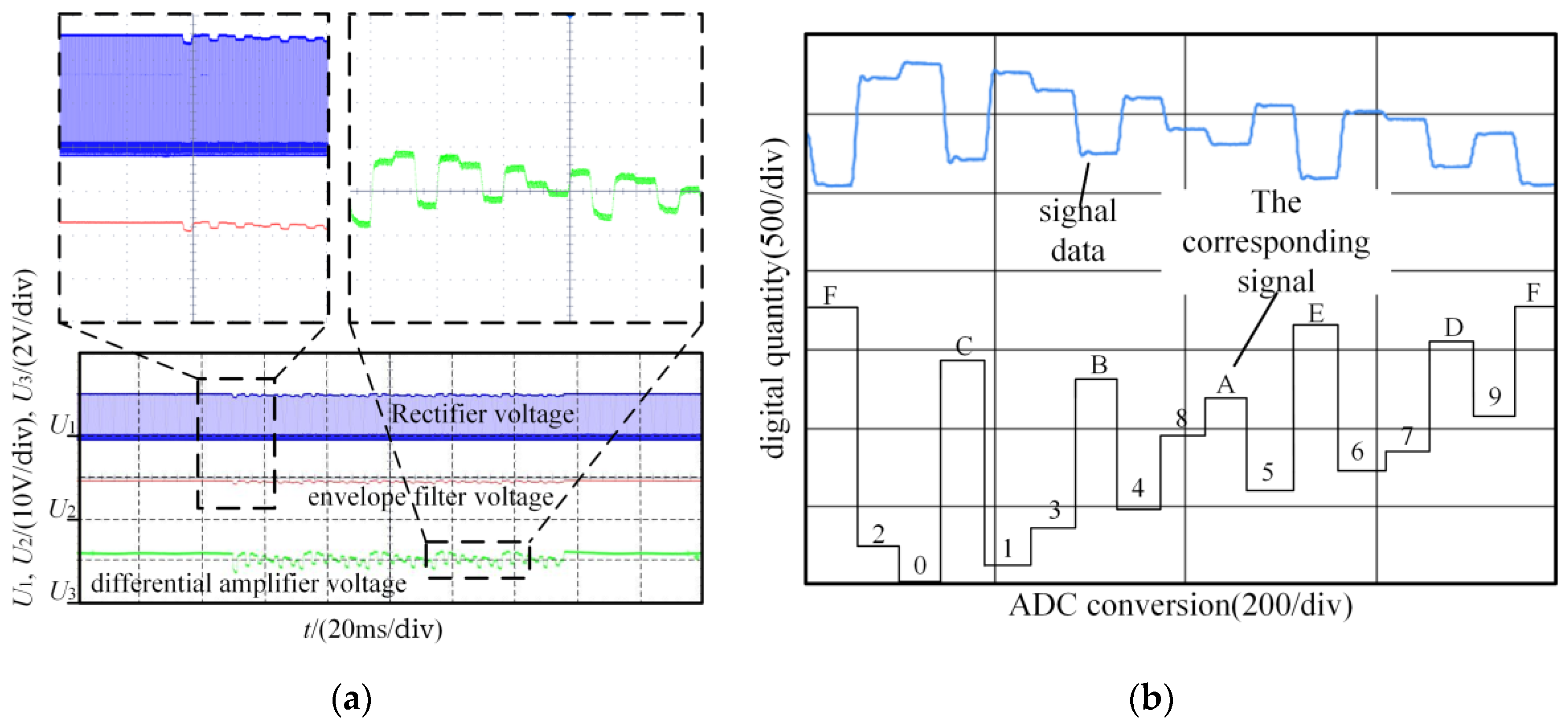
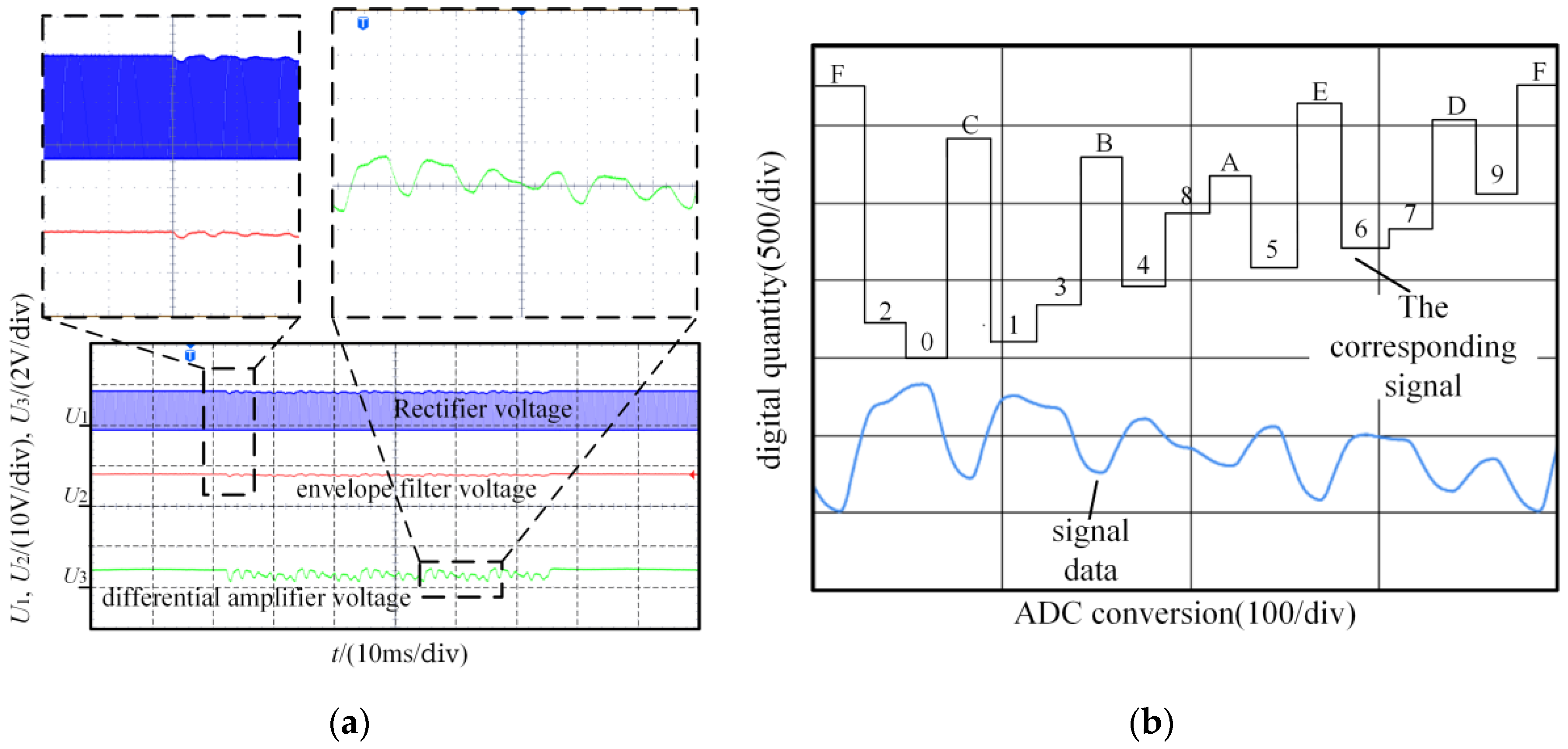
3.2. Signal Demodulation

Signal demodulation is realized by a demodulation circuit and DSP together. The demodulation circuit is shown in Figure 6, including the voltage divider circuit, rectifier circuit, voltage follower, envelope detection circuit, low-pass filter circuit, differential amplifier circuit, protection circuit and so on. First, the collected voltage is divided to protect the chip and device. Through rectifier circuit and voltage follower, the main circuit and subsequent demodulation circuit are isolated to reduce interference. The amplitude change of the high-frequency signal is detected via envelope detection, and the selection of time constant RC of the circuit is very important. After low-pass filtering, the differential amplifier processes the voltage so that the information characteristics of the voltage are fully displayed. Uref is available from chip supply voltage Uo. After low-pass filtering, the processed voltage enters the protection circuit. The circuit selects 2.7 V regulator tube D7. Q1 is not conductive when the input voltage does not exceed 2.7 V. Voltage drops at both ends of GS of Q2, so Q2 turns on. The circuit voltage normal output. When the input voltage is greater than 2.7 V and the excess voltage is greater than the Q1 PN junction conduction voltage, Q1 conduction. The GS voltage across Q2 is equal, so Q2 does not conduct. At this time, the protection circuit is broken, which plays a protective role. After ensuring that the voltage is less than 3 V, the ADC peripheral inside DSP28335 is used to convert the data voltage Udata. The ADC of F28335 meets the demodulation requirements in terms of accuracy and acquisition rate. Finally, the demodulation process can be completed only by judging the converted information data.

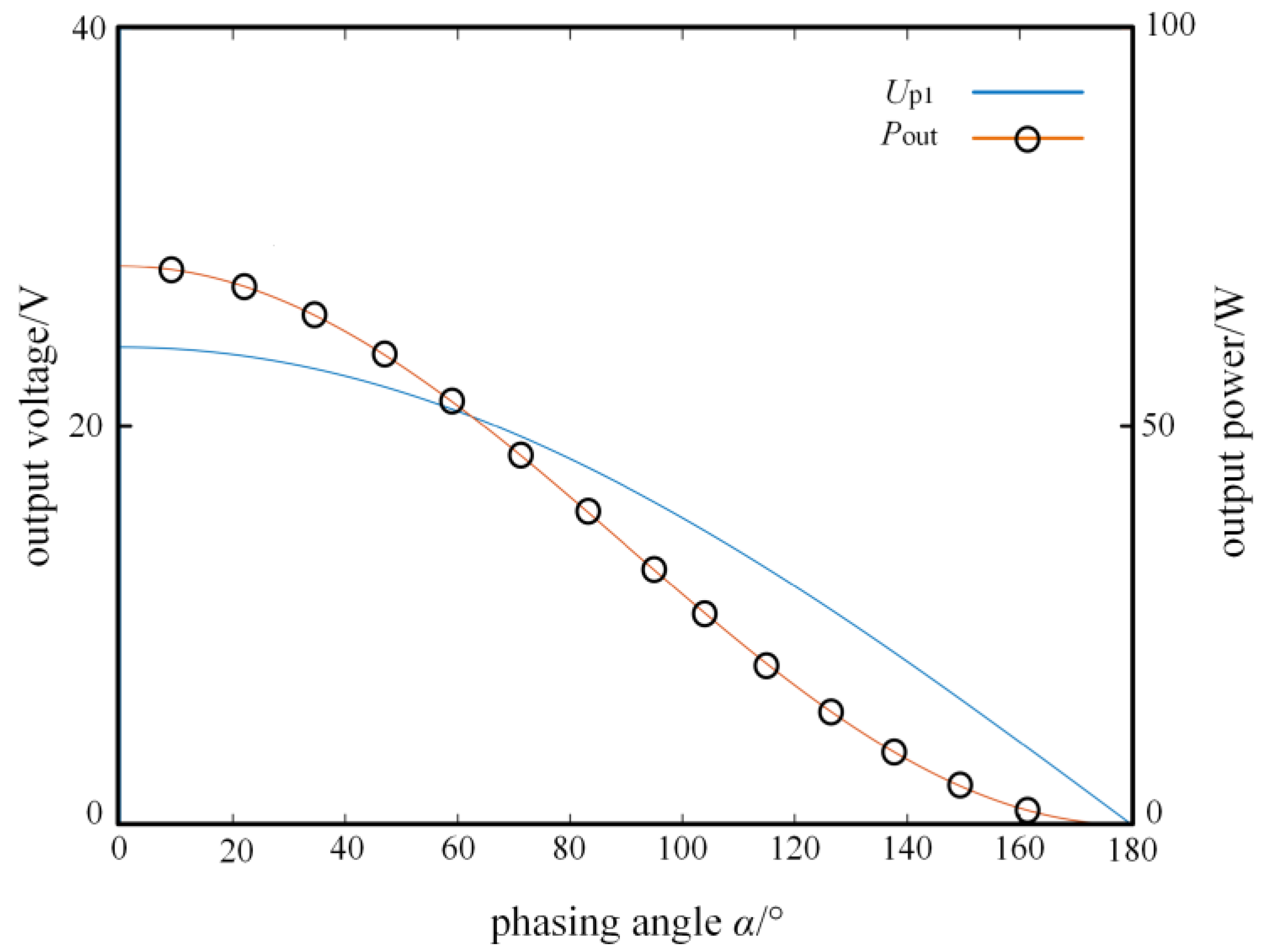
4. System Performance Analysis

4.1. Subsection

Traditional amplitude modulation by adding a Boost circuit before the inverter circuit or to be transmitted baseband signal [20] to control the input voltage amplitude to achieve signal transmission. The voltage fluctuation exceeds 30% of the amplitude during signal transmission, which limits the application of this method. The MASK modulation simultaneous transmission method based on PSFB has the advantages of amplitude modulation: simple structure and no power interference to the signal. At the same time, the demodulation circuit uses a differential amplifier to amplify the signal characteristics in the integrated power signal flow, which can reconcile the contradiction between the output voltage fluctuation and the signal distortion rate and reduce the impact of voltage fluctuation on the system. According to the parameters of Table 2, 8ASK modulation is carried out. For observation purposes, the system transmits the signal ‘01234567’, when the voltage fluctuation at the receiver side is shown in Figure 7, with a voltage fluctuation of about 5%.

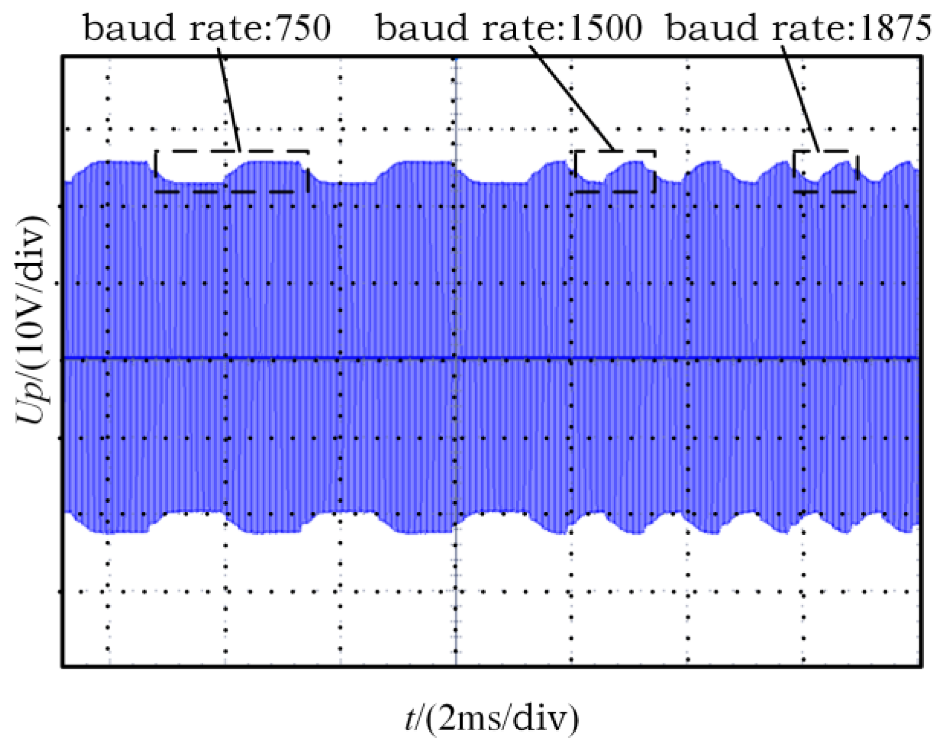
4.2. Analysis of Signal Transmission Rate

Signal transmission rate is used to measure the amount of data transmitted per unit time. The transmission rate is usually expressed by baud rate and bit rate. The numerical relationship between the two is: C = B·log2N, where C is the bit rate, B is the baud rate and N is the base. There are two ways to increase the bit rate from the equation. One way is to increase the baud rate, which can theoretically be up to one-tenth of the carrier frequency. For wireless power transmission systems, the baud rate is limited by the response time of the system itself. Passive devices such as inductors and capacitors can affect the response time of the system. Theoretically, the response speed can only be improved by changing the system device or structure.
The variation law of resonant circuit voltage amplitude with time is:
U p ( t ) = U pm e t τ .
Upm is the inverter output voltage peak. In Figure 1a, τ can be viewed as the Ld discharge time constant in conventional amplitude modulation
τ = R p C p L d L p .
The whole signal ‘0’ modulation process t, voltage change is:
U p ( t ) = U pm ( 1 + e t τ e t T off τ ) .
Toff is the voltage source disconnection time. It can be seen that the existence of Ld affects the time constant τ, and the DC-DC modulation circuit increases the system response time. The MASK modulation simultaneous transmission method based on PSFB improves the system response speed because there is no DC-DC modulation circuit. It controls the voltage amplitude variation at 5% and reduces the amplitude variation, which can reduce the required response time and improve the baud rate of the system itself. As shown in Figure 8, respectively, the baud rate is 750, 1500 and 1875 for data transmission. The results show that when the baud rate is 1875, the rising and falling edges of the signal coincide. After measurement, the response time of the signal is 280 μs. The overall response time of the rise and fall has exceeded the signal time period of 533 μs, which is beyond the limit. The final limit baud rate of the experimental system is about 1500, and the experimental parameters are shown in Table 1.
Another way to increase the transmission rate is to change the transmission system N. By increasing the transmission base, the signal is no longer limited to ‘0’ and ‘1’, increasing the bit width, thereby increasing the signal transmission rate. As shown in Figure 7, using 8ASK signal modulation, compared with the traditional signal transmission method, the signal transmission rate increased to three times.

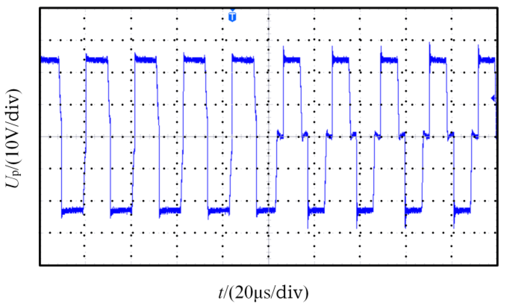
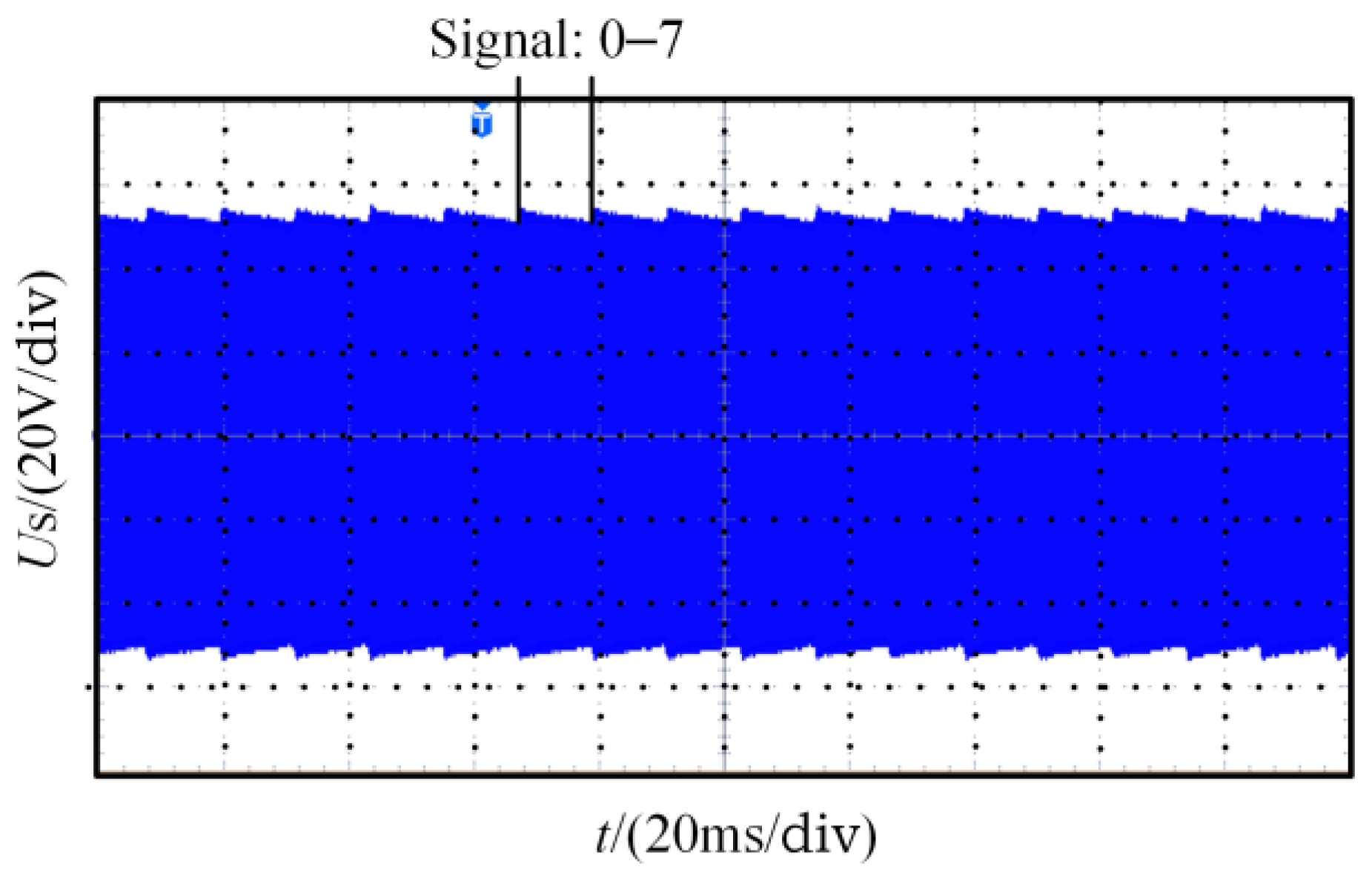
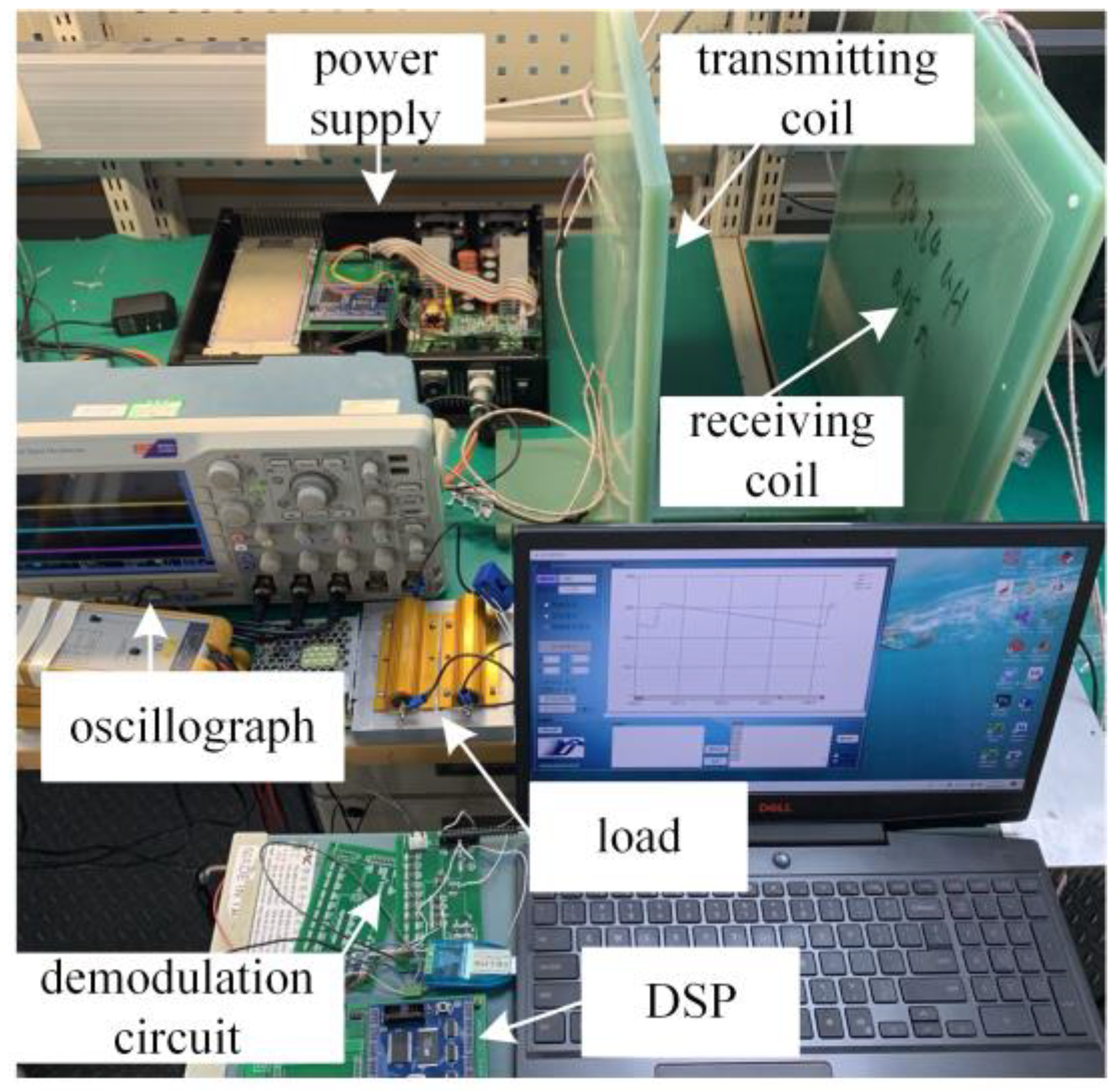
5. Experimental Verification

Based on the proposed power and information synchronous transmission method, an experimental platform is built to verify the MASK modulation power and signal transmission scheme based on PSFB. The experimental platform is shown in Figure 9. The experimental platform consists of a power supply part, a transmitting part and a receiving part. The transmitting part includes transmitting coil and resonant capacitor. The receiving part includes a receiving coil, resonant capacitor, load and signal-extraction part. The system parameters are shown in Table 1 and Table 3.
According to Figure 5 and Table 2, 16ASK modulation is performed. Figure 10 shows the 750 baud rate 16ASK modulation signal transmission. The experiment provided a continuous signal ‘F20C13B48A5E67D9’. The bit rate of information transmission is 3 kbps. Rectifier voltage, envelope filter voltage and differential amplifier voltage waveforms are shown in Figure 10a. R7, R9 is 35 kΩ and R8, R10 is 40 kΩ, so the differential amplifier amplification factor is 1.14. Voltage transferred through the ADC analog-to-digital conversion signal data with the use of a 485 communication in the computer serial assistant is displayed. As shown in Figure 10b, the ADC is a 12-bit precision, and the transmission signal corresponding to the signal data is marked in the figure. The range of ADC acquisition is 3 V, which corresponds to the digital quantity of 4095, and the signal data are about 800. The signal can be obtained by comparing the data or using the algorithm. In the experiment, all the collected data are stored in the array, and the signals are obtained by comparing and judging the data in the array. The transmitting communication unit tests the bit error rate of signal transmission, including 1 bit starting bit, 8 bit data bit and 1 bit stop bit. The method proposed in this paper belongs to amplitude modulation power and information synchronous transmission technology. The signal is reflected and transmitted by the change in voltage amplitude, and the voltage amplitude of the system is affected by many factors, such as the disturbance of the DC power supply, the change in load and the offset of the coupling coil. These factors also affect the signal transmission error rate. The premise of the test is that the system maintains a fixed power output, a fixed load and a fixed position of the two coupling coils. Finally, the test result demonstrates that the signal transmission error rate is 0, and there is no error code in the whole test process.
Figure 11 raises the baud rate to 1500. Signal transmission through 16ASK modulation increases the bit rate to 6 kbps. It can be seen from the diagram that as the baud rate increases, the difficulty of data judgment becomes larger, and error bits may occur. A better data judgment method or algorithm will reduce the bit error rate of the system, which will be a subsequent improvement direction of the signal transmission method.
Demodulation in this paper is essentially envelope detection, which belongs to non-coherent demodulation and is easier to implement than coherent demodulation. Under this demodulation method, the MASK modulation bit error rate is inversely proportional to the signal-to-noise ratio SNR, which is:
SNR = 10 log S N = 20 log V S V N ,
where S is the signal output power, N is the noise power and vs. and VN are the demodulated signal and noise voltage values, respectively. Under the condition that the voltage source output is constant and the signal baud rate is constant, the signal-to-noise ratio and M value affect the bit error rate together. In the experiment, 16ASK modulation is used, and the voltage fluctuation is 5%. Keeping the same signal-to-noise ratio, 8ASK modulation is performed, as shown in Figure 12. With the increase in signal bandwidth, the error rate will be further reduced. If the system continues to increase the signal bit width, that is, to improve the signal bit rate, while maintaining the signal transmission error rate, this can be achieved by increasing the amplification factor of the differential amplifier in the demodulation circuit or adjusting the Uref to improve the signal-to-noise ratio.

6. Conclusions

This paper proposes a MASK modulation power and signals synchronous transmission system based on PSFB. The proposed method reduces the system’s volume without a DC-DC modulation circuit. The proposed method reduces the voltage fluctuation to 5% to minimize the impact of voltage fluctuation on the load. Through the application of a demodulation circuit combined with DSP, it can transmit multiple signals, which are not only limited to ‘0’ and ‘1’. Based on this experimental platform, a 16-band signal can be transmitted, and in different applications, the signal transmission rate may be further improved using this method. This method covers the general audio range and has the prospect of popularization and application.

Author Contributions

Conceptualization, X.Z. and X.P.; methodology, X.Z.; software, X.P.; validation, X.Z., X.P. and Y.G.; formal analysis, Z.C.; investigation, R.H.; resources, M.X.; data curation, X.Z.; writing—original draft preparation, X.P.; writing—review and editing, X.Z.; visualization, Y.G.; supervision, Z.C.; project administration, R.H.; funding acquisition, M.X. All authors have read and agreed to the published version of the manuscript.

Funding

This research was funded by the National Natural Science Foundation of China, grant number 52077153, and the Natural Science Foundation of Tianjin, grant number 20JCYBJC00190.

Institutional Review Board Statement

Not applicable.

Informed Consent Statement

Not applicable.

Data Availability Statement

Not applicable.

Conflicts of Interest

The authors declare no conflict of interest.

References

  1. Luo, C.; Qiu, D.; Gu, W.; Zhang, B.; C’hen, Y.; Xiao, W. Multiload Wireless Power Transfer System With Constant Output Power and Efficiency. IEEE Trans. Ind. Appl. 2021, 58, 1101–1114. [Google Scholar] [CrossRef]
  2. Mao, X.; Chen, J.; Zhang, Y.; Dong, J. A simple and reconfigurable wireless power transfer system with constant voltage and constant current charging. IEEE Trans. Power Electron. 2021, 37, 4921–4925. [Google Scholar] [CrossRef]
  3. Lee, S.B.; Kim, M.; Jang, I.G. Determination of the optimal resonant condition for multireceiver wireless power transfer systems considering the transfer efficiency and different rated powers with altered coupling effects. IEEE J. Emerg. Sel. Top. Power Electron. 2020, 9, 2384–2393. [Google Scholar] [CrossRef]
  4. Yang, L.; Huang, J.; Feng, B.; Zhang, F.; Zhang, Y.; Li, X.; Jian, J.; Wang, Z.; Tong, X. Undersea Wireless Power and Data Transfer System With Shared Channel Powered by Marine Renewable Energy System. IEEE J. Emerg. Sel. Top. Circuits Syst. 2022, 12, 242–250. [Google Scholar] [CrossRef]
  5. Choi, K.W.; Hwang, S.I.; Aziz, A.A.; Jang, H.H.; Kim, J.S.; Kang, D.S.; Kim, D.I. Simultaneous wireless information and power transfer (SWIPT) for Internet of Things: Novel receiver design and experimental validation. IEEE Internet Things J. 2020, 7, 2996–3012. [Google Scholar]
  6. Sedehi, R.; Budgett, D.; Jiang, J.; Ziyi, X.; Dai, X.; Hu, A.P.; McCormick, D. A wireless power method for deeply implanted biomedical devices via capacitively coupled conductive power transfer. IEEE Trans. Power Electron. 2020, 36, 1870–1882. [Google Scholar] [CrossRef]
  7. Hirai, J.; Kim, T.W.; Kawamura, A. Study on intelligent battery charging using inductive transmission of power and information. IEEE Trans. Power Electron. 2000, 15, 335–345. [Google Scholar] [CrossRef]
  8. Kim, J.; Clerckx, B.; Mitcheson, P.D. Signal and system design for wireless power transfer: Prototype, experiment and validation. IEEE Trans. Wirel. Commun. 2020, 19, 7453–7469. [Google Scholar] [CrossRef]
  9. Besnoff, J.; Abbasi, M.; Ricketts, D.S. High data-rate communication in near-field RFID and wireless power using higher order modulation. IEEE Trans. Microw. Theory Tech. 2016, 64, 401–413. [Google Scholar] [CrossRef]
  10. Besnoff, J.; Abbasi, M.; Ricketts, D.S. Ultrahigh-data-rate communication and efficient wireless power transfer at 13.56 MHz. IEEE Antennas Wirel. Propag. Lett. 2017, 16, 2634–2637. [Google Scholar] [CrossRef]
  11. Bieler, T.; Perrottet, M.; Nguyen, V.; Perriard, Y. Contactless power and information transmission. IEEE Trans. Ind. Appl. 2002, 38, 1266–1272. [Google Scholar] [CrossRef]
  12. Rathge, C.; Kuschner, D. High efficient inductive energy and data transmission system with special coil geometry. In Proceedings of the 2009 13th European Conference on Power Electronics and Applications, Barcelona, Spain, 8–10 September 2009; pp. 1–8. [Google Scholar]
  13. Van Boheemen, E.L.; Boys, J.T.; Covic, G.A. Dual-tuning IPT systems for low bandwidth communications. In Proceedings of the 2007 2nd IEEE Conference on Industrial Electronics and Application, Harbin, China, 23–25 May 2007; pp. 586–591. [Google Scholar]
  14. Huang, C.C.; Lin, C.L.; Wu, Y.K. Simultaneous wireless power/data transfer for electric vehicle charging. IEEE Trans. Ind. Electron. 2016, 64, 682–690. [Google Scholar] [CrossRef]
  15. Tang, M.; Jin, Y.; Yao, L. WiFi-ZigBee coexistence based on collision avoidance for wireless body area network. In Proceedings of the 2017 3rd International Conference on Big Data Computing and Communications (BIGCOM), Chengdu, China, 10–11 August 2017; pp. 245–250. [Google Scholar]
  16. Wang, G.; Liu, W.; Sivaprakasam, M.; Zhou, M.; Weiland, J.D.; Humayun, M.S. A dual band wireless power and data telemetry for retinal prosthesis. In Proceedings of the 2006 International Conference of the IEEE Engineering in Medicine and Biology Society, New York, NY, USA, 30 August–3 September 2006; pp. 4392–4395. [Google Scholar]
  17. Wu, J.; Zhao, C.; Lin, Z.; Du, J.; Hu, Y.; He, X. Wireless power and data transfer via a common inductive link using frequency division multiplexing. IEEE Trans. Ind. Electron. 2015, 62, 7810–7820. [Google Scholar] [CrossRef] [Green Version]
  18. Fan, Y.; Sun, Y.; Dai, X.; Zuo, Z.; You, A. Simultaneous wireless power transfer and full-duplex communication with a single coupling interface. IEEE Trans. Power Electron. 2020, 36, 6313–6322. [Google Scholar] [CrossRef]
  19. Li, H.; Chen, S.; Fang, J.; Tang, Y. Synchronous rectification-based phase shift keying communication for wireless power transfer systems. In Proceedings of the 2018 IEEE 4th Southern Power Electronics Conference (SPEC), Singapore, 10–13 December 2018; pp. 1–4. [Google Scholar]
  20. Zhou, J.; Sun, Y.; Su, Y.; Dai, Y.; Zhai, Y. Synchronous transmission of inductively coupled power and signal. J. Chongqing Inst. Technol. (Nat. Sci.) 2009, 23, 93–97. [Google Scholar]
  21. Yan, Z.; Wu, L.; Baoyun, W. High-efficiency coupling-insensitive wireless power and information transmission based on the phase-shifted control. IEEE Trans. Power Electron. 2017, 33, 7821–7831. [Google Scholar] [CrossRef]
  22. Xia, C.; Jia, R.; Wu, Y.; Yu, Q.; Zhou, Y. WPIT technology based on the fundamental-harmonic component for a single-channel and two-coil ICPT system. IET Power Electron. 2019, 12, 2608–2614. [Google Scholar] [CrossRef]
  23. Zhang, Y.; Chen, S.; Li, X.; Tang, Y. Dual-side phase-shift control of wireless power transfer implemented on primary side based on driving windings. IEEE Trans. Ind. Electron. 2020, 68, 8999–9002. [Google Scholar] [CrossRef]
  24. Berger, A.; Agostinelli, M.; Vesti, S.; Oliver, J.A.; Cobos, J.A.; Huemer, M. A wireless charging system applying phase-shift and amplitude control to maximize efficiency and extractable power. IEEE Trans. Power Electron. 2015, 30, 6338–6348. [Google Scholar] [CrossRef]
  25. Lim, Y.; Park, J. A novel phase-control-based energy beamforming techniques in nonradiative wireless power transfer. IEEE Trans. Power Electron. 2014, 30, 6274–6287. [Google Scholar] [CrossRef]
  26. He, X.; Wang, R.; Wu, J.; Li, W. Nature of power electronics and integration of power conversion with communication for talkative power. Nat. Commun. 2020, 11, 2479. [Google Scholar] [CrossRef] [PubMed]
Figure 1. System structure diagram: (a) Traditional amplitude modulation transmission circuit; (b) structure diagram of MASK modulation power and information synchronous transmission system based on PSFB.
Applsci 13 00475 g001
Figure 2. Inverter working waveform.
Applsci 13 00475 g002
Figure 3. System equivalent circuit diagram.
Applsci 13 00475 g003
Figure 4. Inverter output voltage.
Applsci 13 00475 g004
Figure 5. Voltage, power and phase diagram.
Applsci 13 00475 g005
Figure 6. Demodulation circuit diagram.
Applsci 13 00475 g006
Figure 7. Receiving end voltage diagram of power and signal synchronous transmission system.
Applsci 13 00475 g007
Figure 8. System transmission rate diagram.
Applsci 13 00475 g008
Figure 9. Experimental setup.
Applsci 13 00475 g009
Figure 10. A 750 baud rate 16ASK modulation information transmission diagram: (a) Demodulation circuit waveform; (b) ADC conversion voltage data diagram.
Applsci 13 00475 g010
Figure 11. A 1500 baud rate 16ASK modulation information transmission diagram: (a) Demodulation circuit waveform; (b) ADC conversion voltage data diagram.
Applsci 13 00475 g011
Figure 12. Signal demodulation waveform.
Applsci 13 00475 g012
Table 1. Experimental parameters.
ParametersSymbolValue
Power supplyUd24 V
Coil resistanceRp, RS0.1 Ω
Transmitting coil self-inductanceLp282.04 μH
Resonant capacitorCp, CS40 nF
LoadRL35 Ω
Table 2. Signal modulation parameters.
M-ary SignalVoltage AmplitudePhase AngleSignal
8-ary signal100%0
99.28%13.9°1
98.57%19.4°2
97.85%23.9°3
97.14%27.6°4
96.43%30.8°5
95.71%33.8°6
95%36.5°7
16-ary signal100%0
99.67%9.5°1
99.34%13.3°2
99.01%16.2°3
98.68%18.7°4
98.35%21°5
98.02%23°6
97.69%24.8°7
97.36%26.5°8
97.03%28.1°9
96.7%29.6°A
96.37%31.1°B
96.04%32.4°C
95.71%33.8°D
95.38%35.1°E
95%36.5°F
Table 3. Demodulation circuit parameters.
ParametersSymbolValue
ResistancesR1, R122 kΩ
ResistancesR2, R3, R4, R13, R1420 kΩ
ResistancesR5, R6, R11500 Ω
Envelope capacitanceC110 μF
Smoothing capacitancesC2, C3100 nF
Supply voltageUo16 V
Reference voltageUref8 V
Disclaimer/Publisher’s Note: The statements, opinions and data contained in all publications are solely those of the individual author(s) and contributor(s) and not of MDPI and/or the editor(s). MDPI and/or the editor(s) disclaim responsibility for any injury to people or property resulting from any ideas, methods, instructions or products referred to in the content.

