
Constraints of Using Conductive Screen-Printing for Chipless RFID Tags with Enhanced RCS Response

Abstract
:1. Introduction
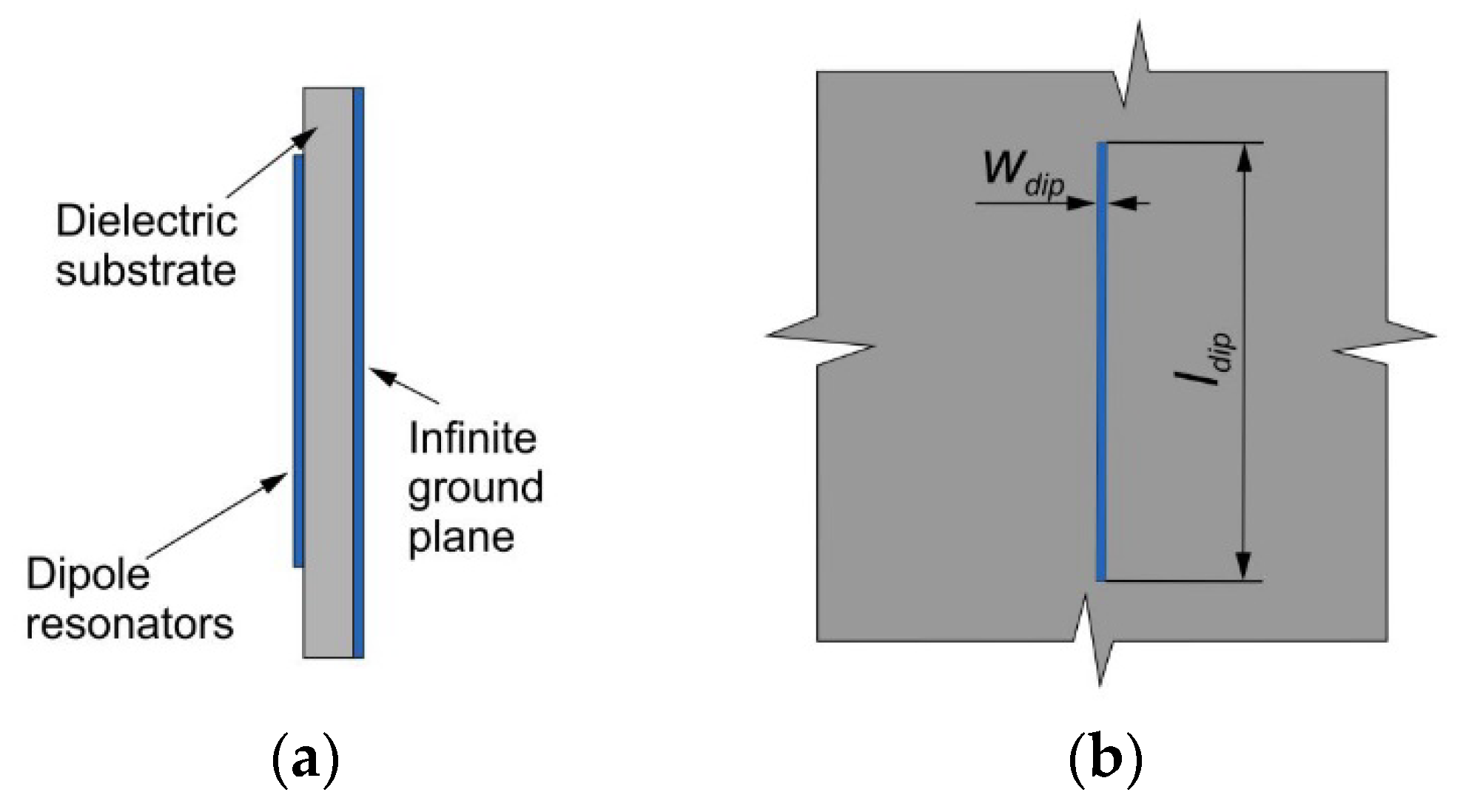
2. Theoretical Background
- (1)
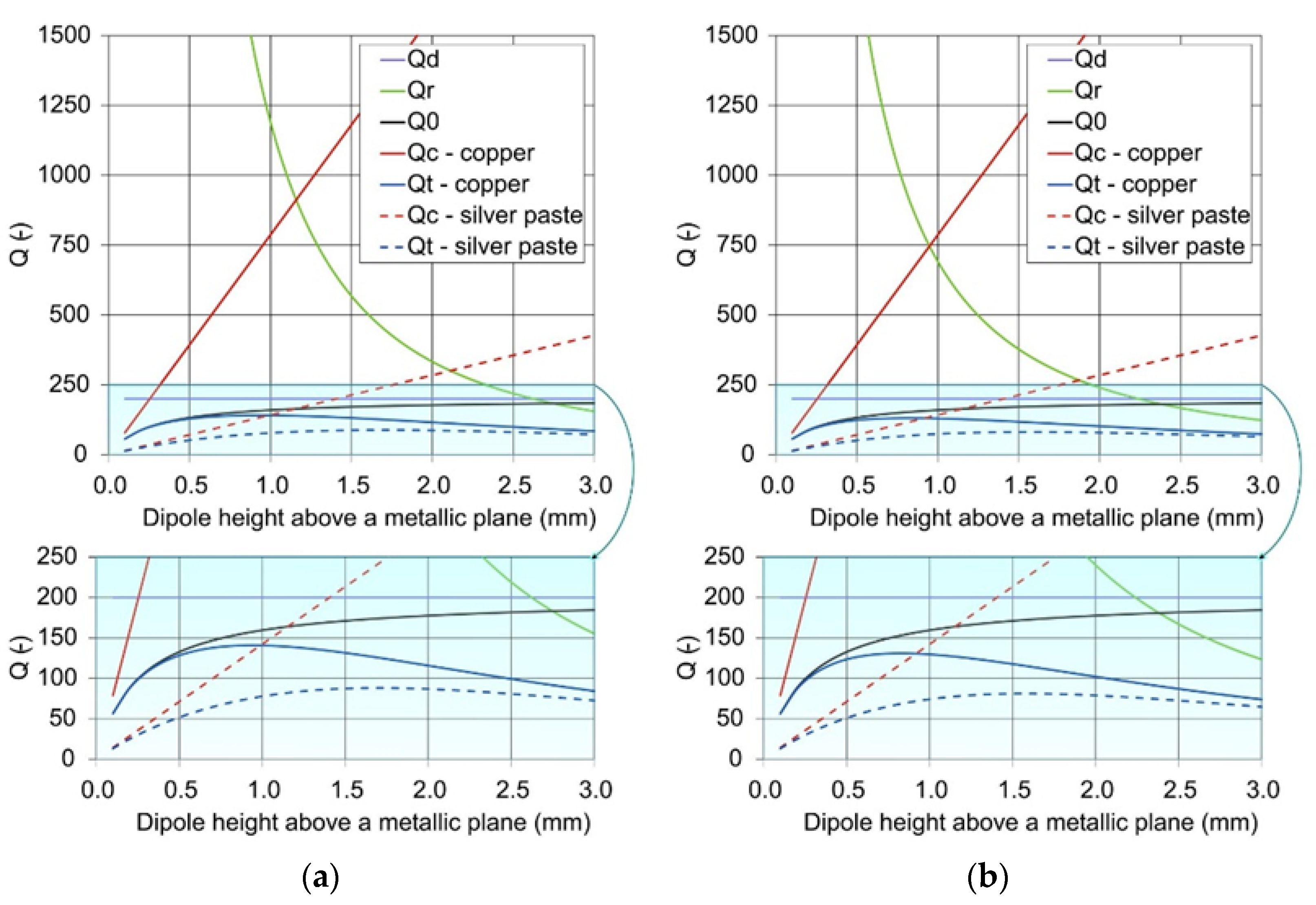
- , under-coupled,
- (2)
- , over-coupled,
- (3)
- , critically-coupled.
3. Tags with Enhanced RCS Response
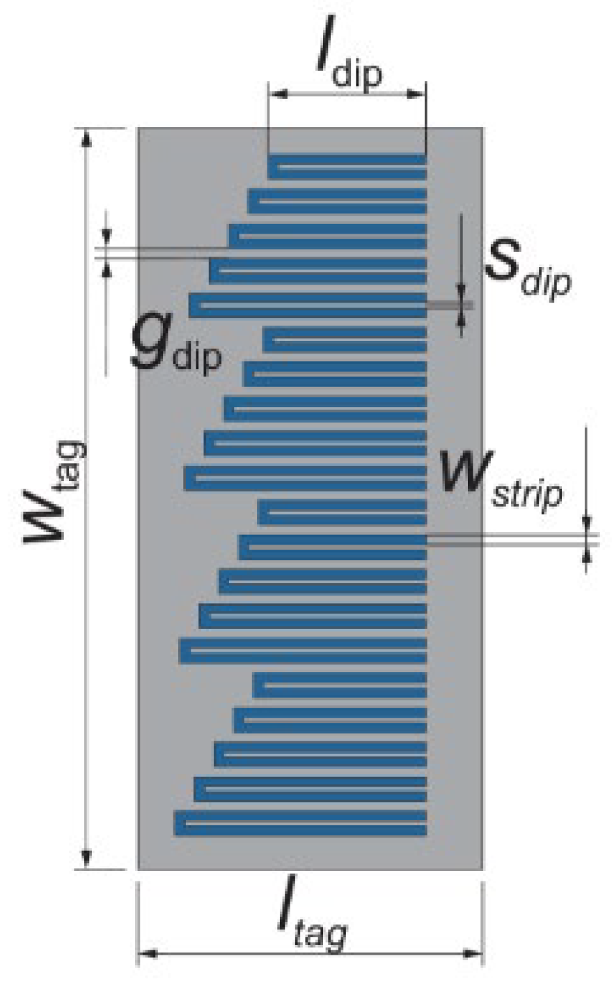
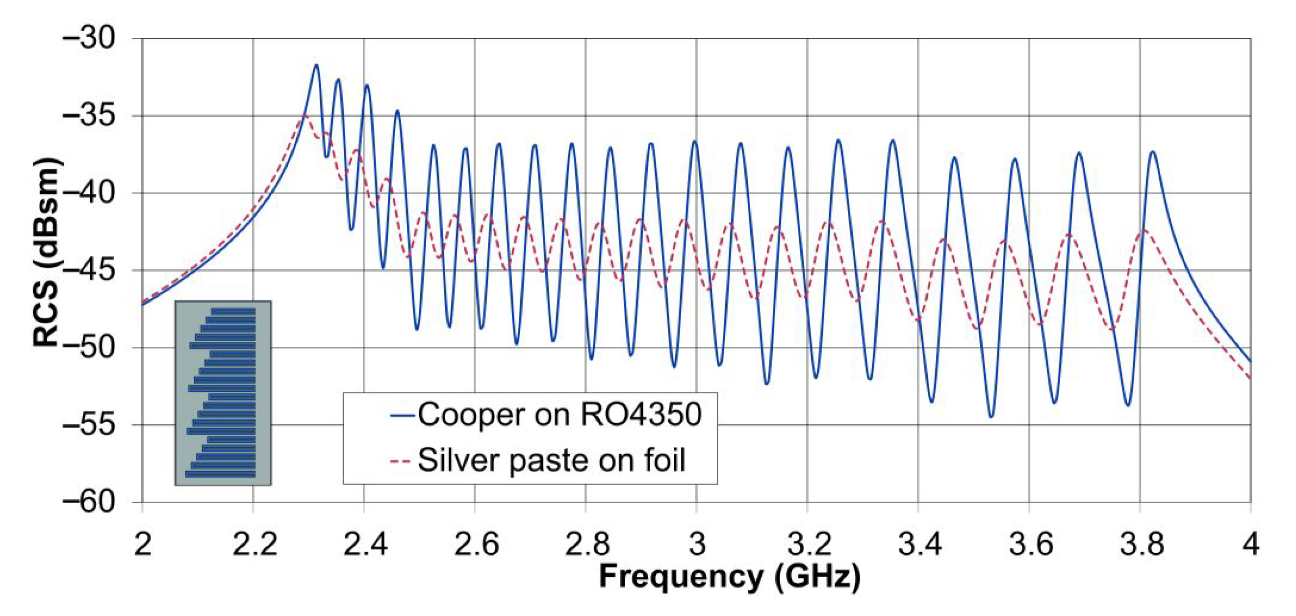
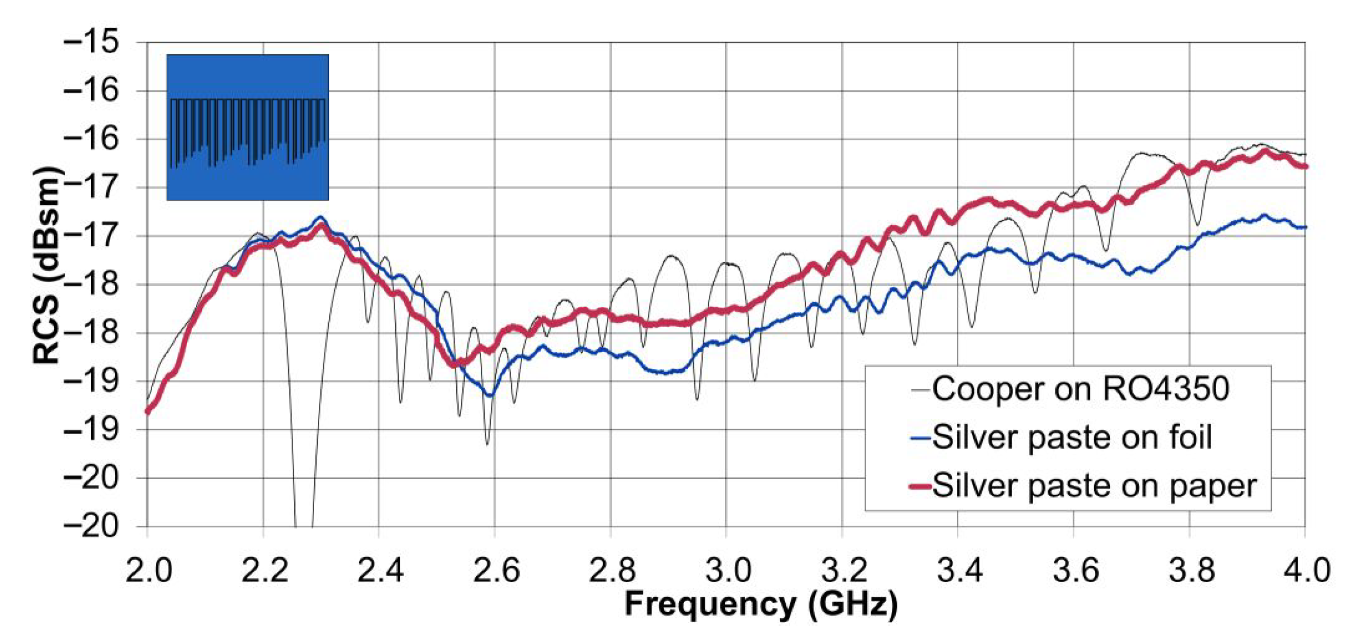
3.1. Re-Arranged Shorted U-Dipoles
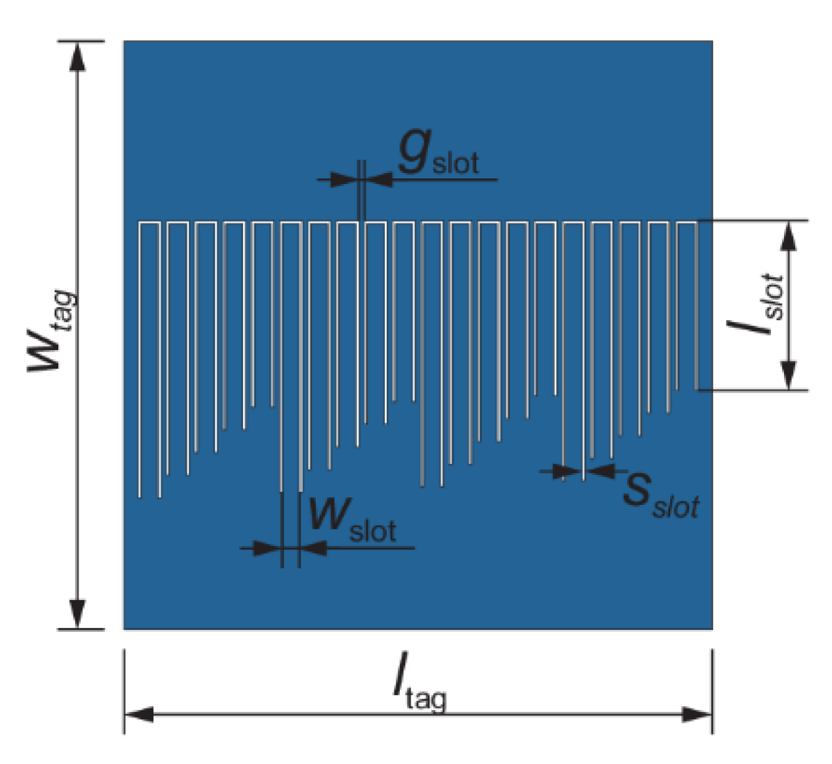
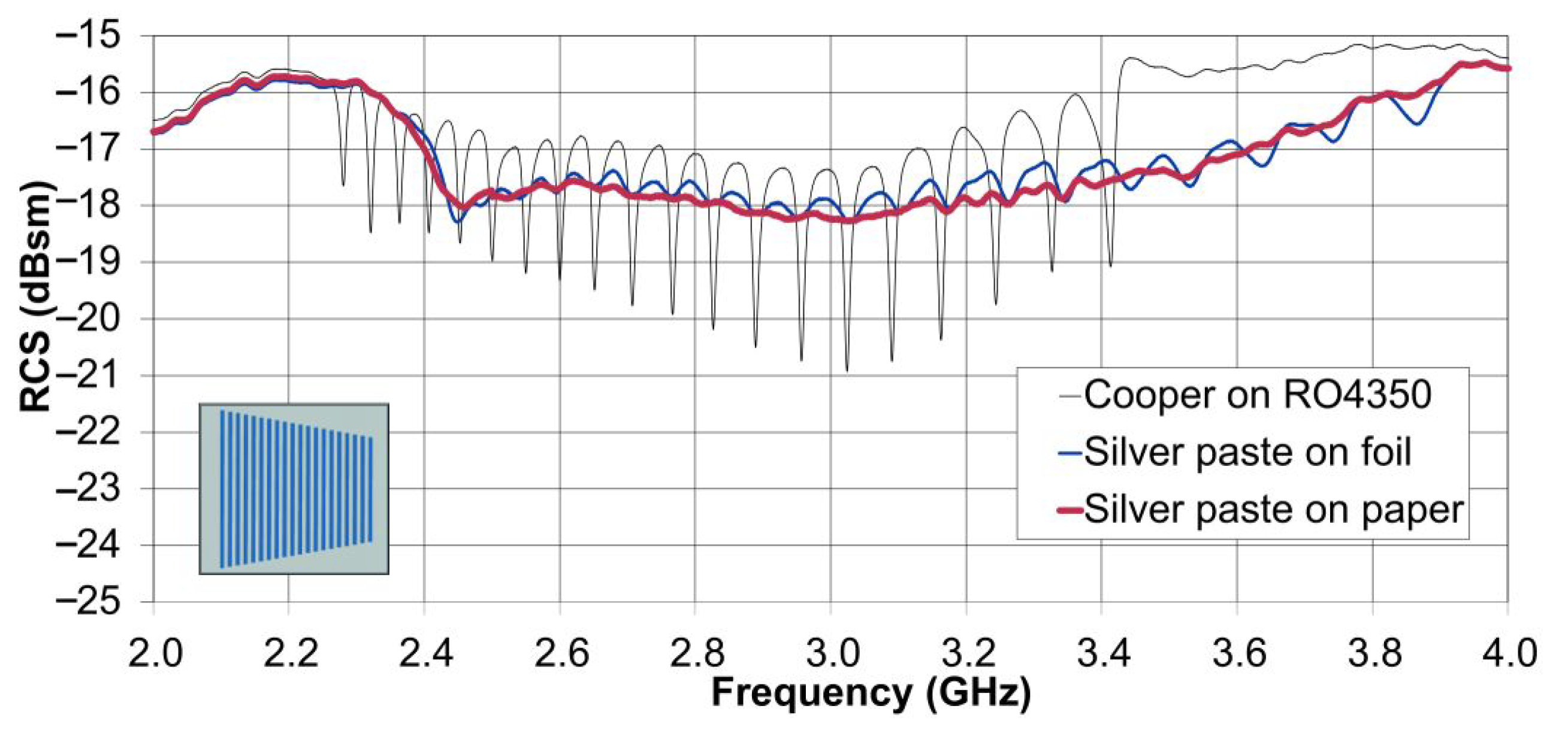
3.2. Re-Arranged U-Slots in the Metallic Plate
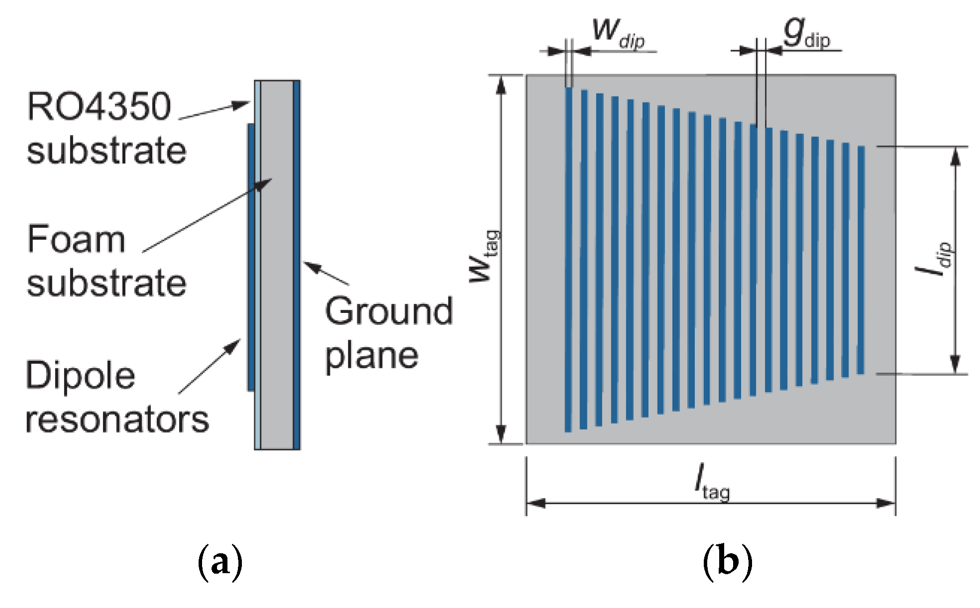
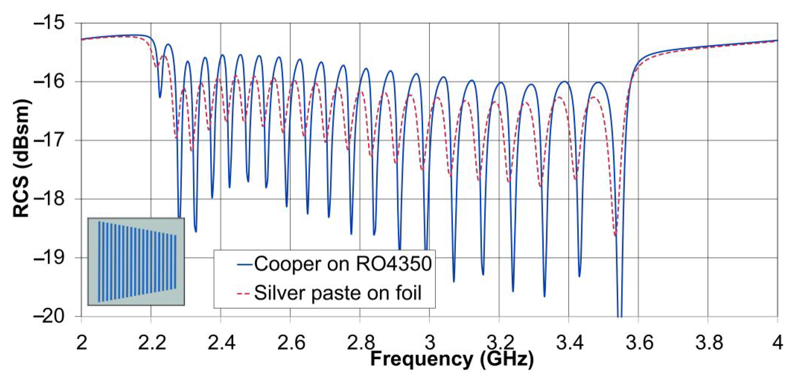
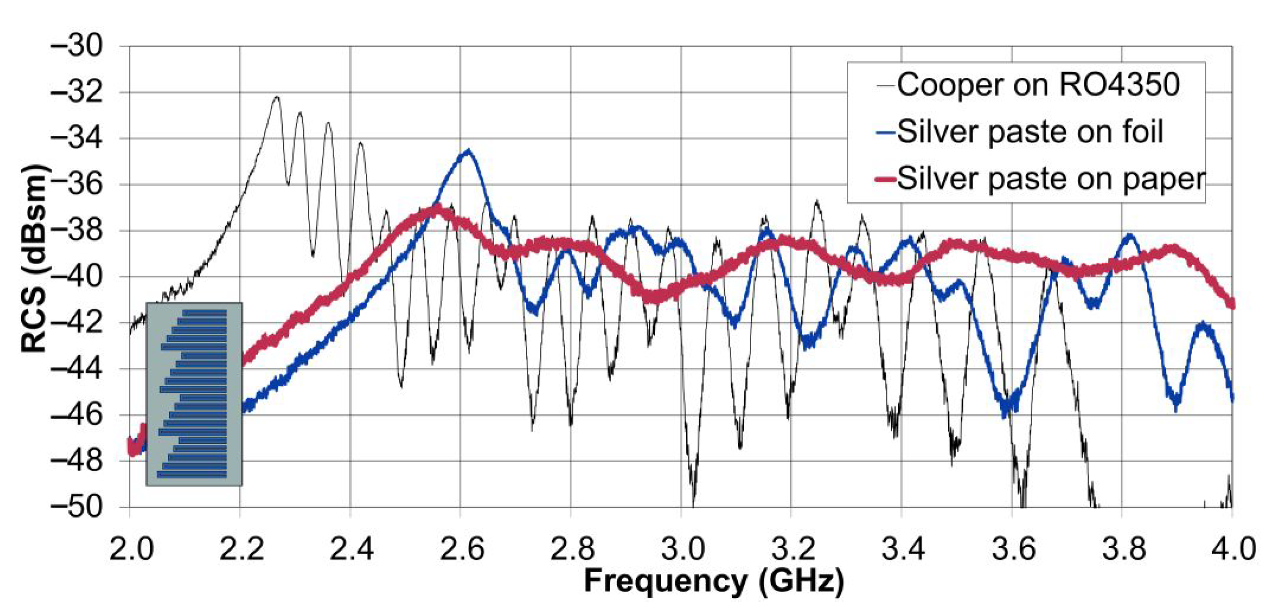
3.3. Array of Detuned Planar Dipoles Closely Coupled to a Rectangular Metallic Plate
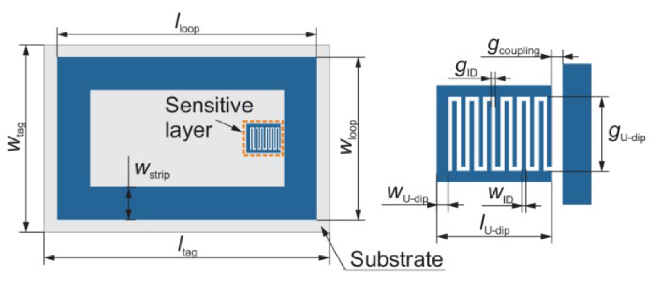
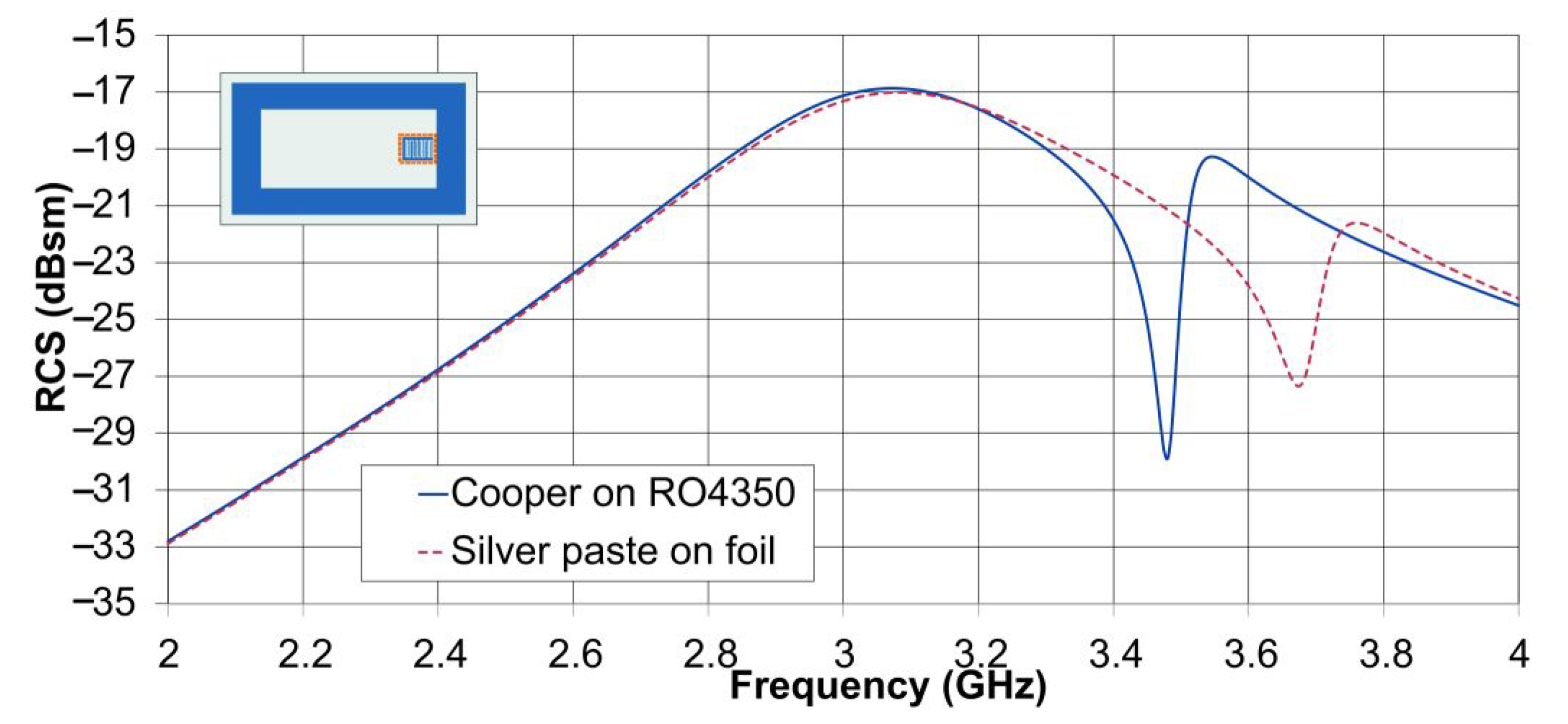
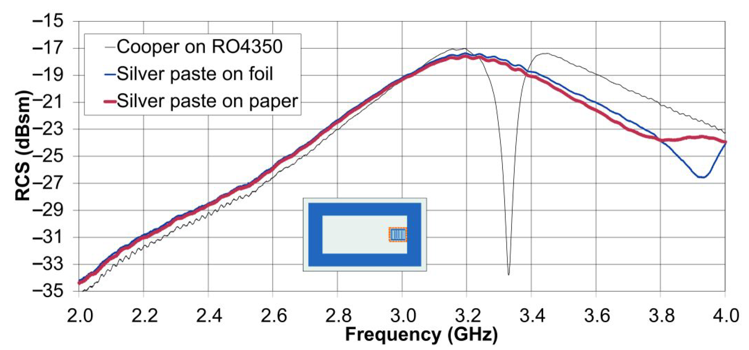
3.4. Interdigital U-Dipole Coupled to the Metallic Loop
4. Conductive Screen-Printing of the Tags with Enhanced RCS Response
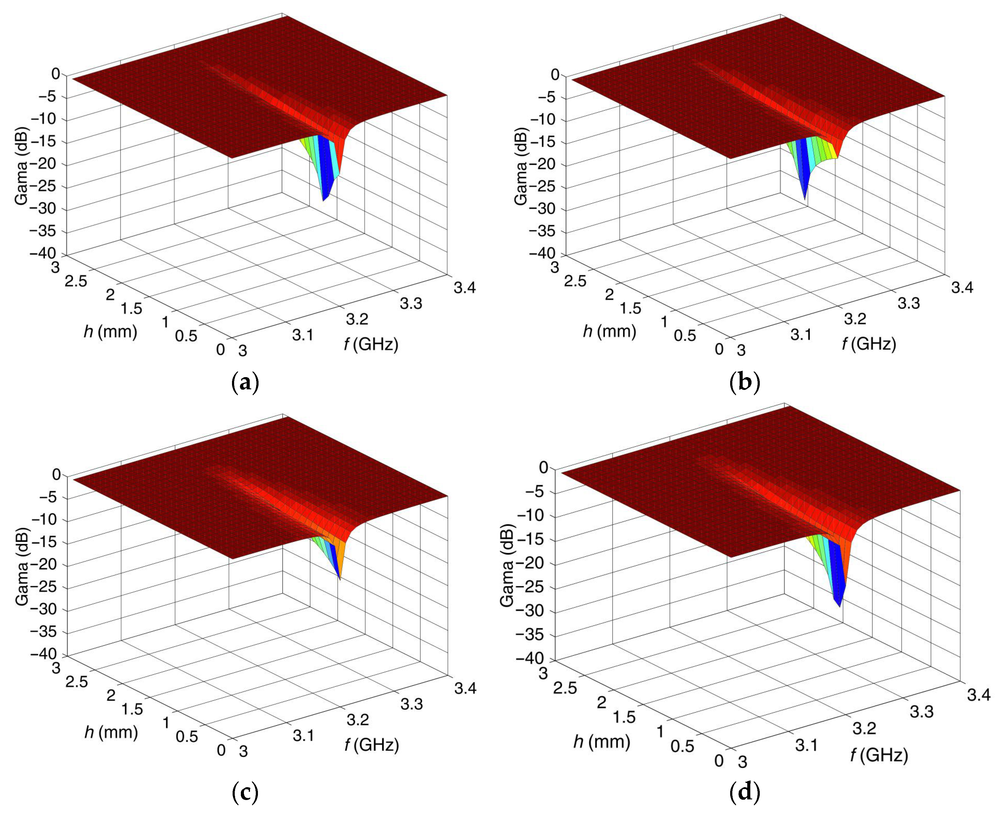
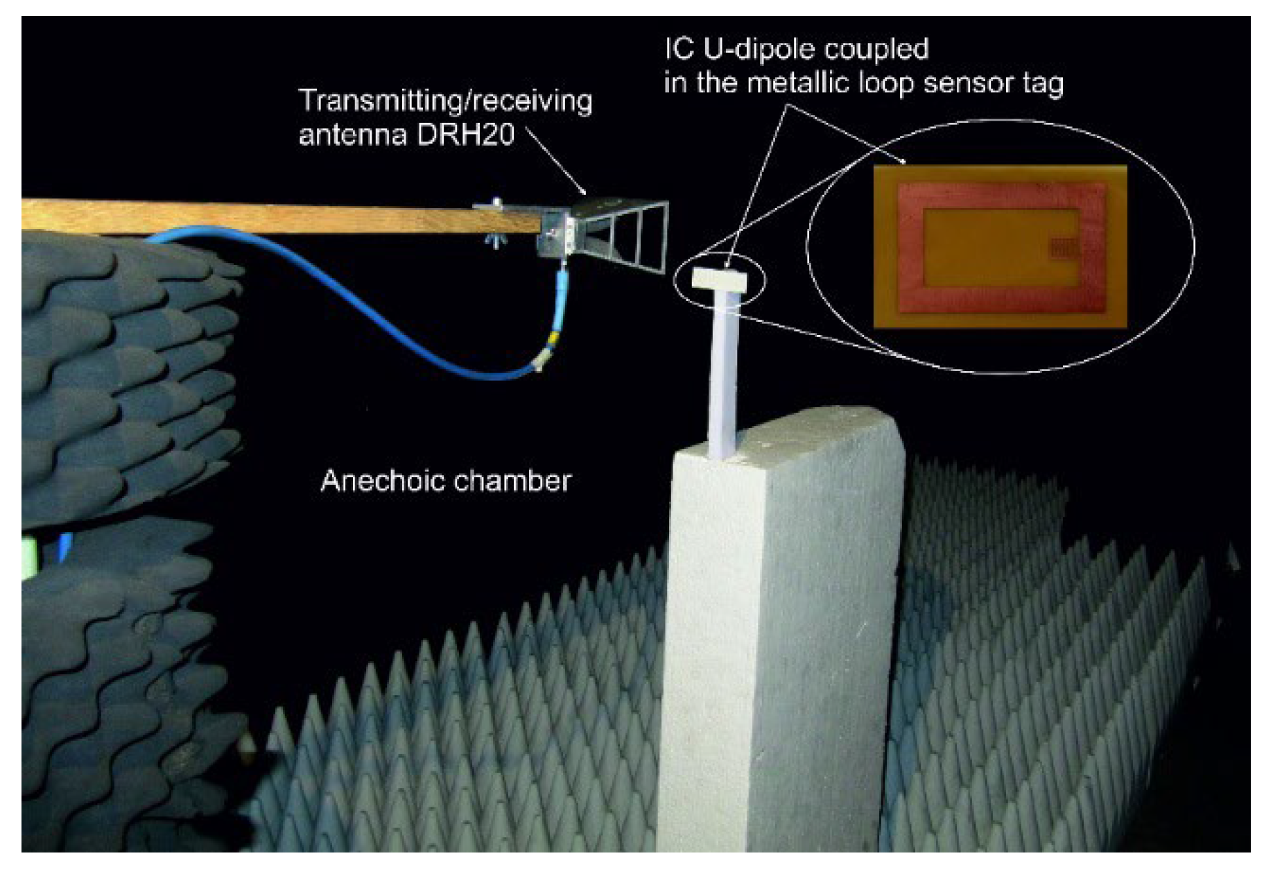
5. Measurement
6. Conclusions
Author Contributions
Funding
Institutional Review Board Statement
Informed Consent Statement
Data Availability Statement
Acknowledgments
Conflicts of Interest
References
- Finkenzeller, K. RFID Handbook: Fundamentals and Applications in Contactless Smart Cards and Identification, 2nd ed.; John Wiley & Sons: Hoboken, NJ, USA, 2005. [Google Scholar]
- Babar, A.A.; Bjorninen, T.; Bhagavati, V.A.; Sydanheimo, L.; Kallio, P.; Ukkonen, L. Small and flexible metal mountable passive UHF RFID tag on high-dielectric polymer-ceramic composite substrate. IEEE Antennas Wirel. Propag. Lett. 2012, 11, 1319–1322. [Google Scholar] [CrossRef]
- Marrocco, G. RFID antennas for the UHF remote monitoring of human subjects. IEEE Trans. Antennas Propag. 2007, 55, 1862–1870. [Google Scholar] [CrossRef] [Green Version]
- Svanda, M.; Polivka, M. Two novel extremely low-profile slot-couplet two-element patch antennas for UHF RFID of people. Microw. Opt. Technol. Lett. 2010, 52, 249–252. [Google Scholar] [CrossRef]
- Svanda, M.; Polivka, M.; Hudec, P. Novel low-profile foam dielectric over-the-shoulder antenna based on coupled patches technique. Microw. Opt. Technol. Lett. 2013, 55, 593–597. [Google Scholar] [CrossRef]
- Occhiuzzi, C.; Caizzone, S.; Marrocco, G. Passive UHF RFID antennas for sensing applications: Principles, methods and classifications. IEEE Antennas Propag. Mag. 2014, 55, 14–34. [Google Scholar] [CrossRef] [Green Version]
- Kracek, J.; Švanda, M.; Mazanek, M.; Machac, J. Implantable semi-active UHF RFID tag with inductive wireless power transfer. IEEE Antennas Wirel. Propag. Lett. 2016, 15, 1657–1660. [Google Scholar] [CrossRef]
- Carvalho, N.B.; Georgiadis, A.; Costanzo, A.; Stevens, N.; Kracek, J.; Pessoa, L.M.; Roselli, L.; Dualibe, F.; Schreurs, D.; Mutlu, S.; et al. Europe and the Future for WPT COST Action IC1301 Team. IEEE Microw. Mag. 2017, 18, 56–87. [Google Scholar]
- Occhuizzi, C. RFID Passive gas sensor integrating carbon nanotubes. IEEE Trans. Microw. Theory Tech. 2011, 59, 2674–2684. [Google Scholar] [CrossRef]
- Karmakar, N.C. Tag, you’re it radar cross section of chipless RFID tags. IEEE Microw. Mag. 2016, 17, 64–74. [Google Scholar] [CrossRef]
- Vena, A.; Perret, E.; Tedjini, S. A fully printable chipless RFID tag with detuning correction technique. IEEE Microw. Wirel. Compon. Lett. 2012, 22, 209–211. [Google Scholar] [CrossRef]
- Rance, O.; Siragusa, R.; Lemaitre-Auger, P.; Perret, E. Toward RCS magnitude level coding for chipless RFID. IEEE Trans. Microw. Theory Tech. 2016, 64, 2315–2325. [Google Scholar] [CrossRef]
- Polivka, M.; Havlicek, J.; Svanda, M.; Machac, J. Improvement in robustness and recognizability of RCS response of U-shaped strip-based chipless RFID tags. IEEE Antennas Wirel. Propag. Lett. 2016, 15, 2000–2003. [Google Scholar] [CrossRef]
- Polivka, M.; Svanda, M.; Machac, J. Chipless RFID tag with an improved rcs response. In Proceedings of the European Microwave Week 2014 (44th EuMC, EuRAD, EuMIC, EuWT) [CD-ROM], Rome, Italy, 6–9 October 2014. [Google Scholar]
- Havlicek, J.; Svanda, M.; Polivka, M.; Machac, J.; Kracek, J. Chipless RFID tag based on electrically small spiral capacitively loaded dipole. IEEE Antennas Wirel. Propag. Lett. 2017, 16, 3051–3054. [Google Scholar] [CrossRef]
- Huang, H.; Su, L. A compact dual-polarized chipless RFID tag by using nested concentric square loops. IEEE Antennas Wirel. Propag. Lett. 2017, 16, 1036–1039. [Google Scholar] [CrossRef]
- Added, M.; Boulejfen, N.; Svanda, M.; Ghannouchi, F.M.; Vuong, T.-P. High-Performance chipless radio-frequency identification tags: Using a slow-wave approach for miniaturized structure. IEEE Antennas Propag. Mag. 2019, 61, 46–54. [Google Scholar] [CrossRef]
- Costa, F.; Genovesi, S.; Monorchio, A. A chipless RFID based on multiresonant high-impedance surfaces. IEEE Trans. Microw. Theory Tech. 2013, 61, 146–152. [Google Scholar] [CrossRef]
- Kracek, J.; Svanda, M.; Hoffmann, K. Scalar method for reading of chipless rfid tags based on limited ground plane backed dipole resonator array. IEEE Trans. Microw. Theory Tech. 2019, 67, 4547–4558. [Google Scholar] [CrossRef]
- Genovesi, S.; Costa, F.; Dicandia, F.A.; Borgese, M.; Manara, G. Orientation-insensitive and normalization-free reading chipless rfid system based on circular polarization interrogation. IEEE Trans. Antennas Propag. 2020, 68, 2370–2378. [Google Scholar] [CrossRef]
- Špůrek, J.; Raida, Z.; Láčík, J.; Mikulášek, T.; Vélim, J.; Prášek, J. Circular slot antenna array printed on 3d textile substrate. Elektrorevue 2017, 19, 140–144. [Google Scholar]
- Yang, L.; Rida, A.; Vyas, R.; Tentzeris, M.M. RFID tag and rf structures on a paper substrate using inkjet-printing technology. IEEE Trans. Microw. Theory Tech. 2007, 55, 2894–2901. [Google Scholar] [CrossRef] [Green Version]
- Tehrani, B.K.; Cook, B.S.; Tentzeris, M.M. Inkjet printing of multilayer millimeter-wave yagi-uda antennas on flexible substrates. IEEE Antennas Wirel. Propag. Lett. 2016, 15, 143–146. [Google Scholar] [CrossRef]
- Whittow, W.G.; Chauraya, A.; Vardaxoglou, J.C.; Li, Y.; Torah, R.; Yang, K.; Beeby, S.; Tudor, J. Inkjet-printed microstrip patch antennas realized on textile for wearable applications. IEEE Antennas Wirel. Propag. Lett. 2014, 13, 71–74. [Google Scholar] [CrossRef]
- Rashidian, A.; Shafai, L.; Sobociński, M.; Peräntie, J.; Juuti, J.; Jantunen, H. Printable planar dielectric antennas. IEEE Trans. Antennas Propag. 2016, 64, 403–413. [Google Scholar] [CrossRef]
- Sun, H.; Xiao, G.; Lang, S.; Zhang, Z.; Tao, Y. Screen Printed HF RFID Antennas on Polyethylene Terephthalate Film. IEEE J. Radio Freq. Identif. 2019, 3, 91–97. [Google Scholar] [CrossRef]
- Balanis, C.A. Antenna Theory, Analysis and Design, 2nd ed.; John Wiley & Sons, Inc.: New York, NY, USA, 1997. [Google Scholar]
- Sten, J.C.E.; Hujanen, A.; Koivisto, P.K. Quality factor of an electrically small antenna radiating close to a conducting plane. IEEE Trans. Antennas Propag. 2001, 49, 829–837. [Google Scholar] [CrossRef]
- Best, S.R. Improving performance properties of a dipole element closely spaced to a PEC ground plane. IEEE Antennas Wirel. Propag. Lett. 2004, 3, 359–363. [Google Scholar] [CrossRef]
- Chang, H.C.; Cho, Y.H.; Kwon, D.-H. Radiation Q bounds for small electric dipoles over a conducting ground plane. IEEE Trans. Antennas Propag. 2014, 62, 2031–2040. [Google Scholar] [CrossRef]
- Hazdra, P.; Capek, M.; Eichler, J.; Mazanek, M. The radiation Q factor of a horizontal λ/2 dipole above ground plane. IEEE Antennas Wirel. Propag. Lett. 2014, 13, 1073–1075. [Google Scholar] [CrossRef]
- Jackson, D.R. Microstrip antennas. In Antenna Engineering Handbook; Volakis, J.L., Ed.; McGraw Hill: New York, NY, USA, 2007. [Google Scholar]
- Svanda, M.; Polivka, M.; Havlicek, J.; Machac, J.; Werner, D.H. Platform tolerant, high encoding capacity dipole array-plate chipless RFID tags. IEEE Access 2019, 7, 138707–138720. [Google Scholar] [CrossRef]
- Svanda, M.; Polivka, M.; Havlicek, J.; Machac, J. Chipless RFID tag with an improved magnitude and robustness of RCS response. Microw. Opt. Technol. Lett. 2017, 59, 488–492. [Google Scholar] [CrossRef]
- Svanda, M.; Machac, J.; Polivka, M.; Havlova, S.; Fitl, P.; Vrnata, M. Chipless RFID tag with enhanced RCS used as phthalocyanine chemical gas sensor. IEEE Antennas Wirel. Propag. Lett. 2020, 19, 1556–1560. [Google Scholar] [CrossRef]
- Ayadi, H.; Machac, J.; Svanda, M.; Boulejfen, N.; Latrach, L. Proof-of-Concept of Reconfigurable Solvent Vapors Sensor Tag with Wireless Power Transfer for IoT Applications. Appl. Sci. 2022, 12, 10266. [Google Scholar] [CrossRef]
- Model DRH20—Double Ridge Waveguide Horn. RFspin s.r.o. Available online: http://www.rfspin.cz/en/antennas/drh20.php (accessed on 10 March 2022).


| ltag (mm) | wtag (mm) | ldip (mm) | gdip (mm) | sdip (mm) | wstip (mm) |
|---|---|---|---|---|---|
| 35 | 75 | 14.8 to 24.3 | 1 | 0.5 | 1 |
| ltag (mm) | wtag (mm) | lslot (mm) | gslot (mm) | sslot (mm) | wslot (mm) |
|---|---|---|---|---|---|
| 52 | 50 | 13 to 22.5 | 0.5 | 0.25 | 1.5 |
| ltag (mm) | wtag (mm) | ldip (mm) | gdip (mm) | wdip (mm) |
|---|---|---|---|---|
| 60 | 60 | 31.5 to 50.5 | 1.5 | 1 |
| ltag (mm) | wtag (mm) | lloop (mm) | wloop (mm) | wstrip (mm) | lU-dip (mm) |
|---|---|---|---|---|---|
| 50 | 32 | 40 | 25 | 5 | 5.3 |
| wU-dip (mm) | wID (mm) | gU-dip (mm) | gID (mm) | gcoupling (mm) | N (-) |
| 0.5 | 0.2 | 3.4 | 0.25 | 2 | 7 |
| Resonator Type [Reference] | Frequency Range (GHz) | Number of Bits | Spatial Density at Center Freq. (bit/λ2) | Spectral Capacity (bit/GHz) | Encoding Capacity (bit/λ2/GHz) | RCS (dBsm) | Platform Tolerance | Number of Metallic Layers | Peak Depth—DPS Technology (dB) | Peak Depth—Screen-Printing (dB) | Peak Depth Screen-Print./DPS Ratio (dB) |
|---|---|---|---|---|---|---|---|---|---|---|---|
| Re-arranged shorted U-dipoles [13] | 2.2–3.8 | 20 | 112.0 | 12.5 | 70.0 | −35 | No | 1 | 4 | - | - |
| Re-arranged U-slots in the metallic plate [34] | 2.2–3.8 | 20 | 76.9 | 12.5 | 48.1 | −17 | No | 1 | 1 | - | - |
| Array of detuned planar dipoles closely coupled to a rectangular metallic plate [33] | 2.2–3.5 | 20 | 61.6 | 15.4 | 47.4 | −15 | Yes | 2 | 2 | 0.5 | −1.5 |
| Interdigital U-dipole coupled to the metallic loop sensor tag [35] | 2.6–3.6 | 1 | 5.3 | - | - | −17 | No | 1 | 17 | 4 | −13 |
Disclaimer/Publisher’s Note: The statements, opinions and data contained in all publications are solely those of the individual author(s) and contributor(s) and not of MDPI and/or the editor(s). MDPI and/or the editor(s) disclaim responsibility for any injury to people or property resulting from any ideas, methods, instructions or products referred to in the content. |
© 2022 by the authors. Licensee MDPI, Basel, Switzerland. This article is an open access article distributed under the terms and conditions of the Creative Commons Attribution (CC BY) license (https://creativecommons.org/licenses/by/4.0/).
Share and Cite
Svanda, M.; Machac, J.; Polivka, M. Constraints of Using Conductive Screen-Printing for Chipless RFID Tags with Enhanced RCS Response. Appl. Sci. 2023, 13, 148. https://doi.org/10.3390/app13010148
Svanda M, Machac J, Polivka M. Constraints of Using Conductive Screen-Printing for Chipless RFID Tags with Enhanced RCS Response. Applied Sciences. 2023; 13(1):148. https://doi.org/10.3390/app13010148
Chicago/Turabian StyleSvanda, Milan, Jan Machac, and Milan Polivka. 2023. "Constraints of Using Conductive Screen-Printing for Chipless RFID Tags with Enhanced RCS Response" Applied Sciences 13, no. 1: 148. https://doi.org/10.3390/app13010148