Article

A Resonant Ring Topology Approach to Power Line Communication Systems within Photovoltaic Plants

by
José Ignacio Morales-Aragonés
1,
Matthew St. Michael Williams
2,
Víctor Alonso Gómez
1,
Sara Gallardo-Saavedra
3,
Alberto Redondo-Plaza
3,
Diego Fernández-Martínez
3,
Francisco José Sánchez-Pacheco
4,
Juan Gabriel Fajardo Cuadro
5 and
Luis Hernández-Callejo
6,*
1
Departamento de Física, Universidad de Valladolid, 42004 Soria, Spain
2
Climate Studies Group Mona (CSGM), Department of Physics, University of the West Indies, Kingston 07, Jamaica
3
Departamento Ingeniería Agrícola y Forestal, Universidad de Valladolid, 42004 Soria, Spain
4
Departamento de Tecnología Electrónica, Universidad de Málaga, 29010 Málaga, Spain
5
Departamento de Ingeniería Mecánica, Universidad Tecnológica de Bolivar, Cartagena de Indias 130001, Colombia
6
ADIRE-ITAP, Departamento Ingeniería Agrícola y Forestal, Universidad de Valladolid, 42004 Soria, Spain
*
Author to whom correspondence should be addressed.
Appl. Sci. 2022, 12(16), 7973; https://doi.org/10.3390/app12167973
Submission received: 18 July 2022 / Revised: 2 August 2022 / Accepted: 8 August 2022 / Published: 9 August 2022
(This article belongs to the Topic Advances in Renewable Energy and Energy Storage)

Abstract

:
Within this study, single-cable propagation facilitated by PV strings’ wiring characteristics is considered for an adapted design of PLC electronics. We propose to close the communications signal path, resulting in a ring topology where a resonance condition could be implemented. A PLC topology using the resulting circular closed-loop path of a PV series string as its physical communication support is designed and leveraged for practical use. When the path length or the number of transceivers is changed, the resonance properties that come with the circular path as the physical support are affected but are shown to be preserved with the application of automatic adjustable tuning. This automatic tuning guarantees that the resonance improves propagation parameters and reverts the system to its optimal values at the chosen carrier frequency.

1. Introduction

Monitoring and maintenance tasks within solar plants are becoming the focus of many research efforts, and a growing number of sensors and measuring devices are proposed to be installed along different points of the solar module associations, even within each solar module [1]. In this scenario, communications between solar modules and centralization points (combiner boxes) become an essential subject for research. Considering the year-on-year growing amount of solar modules within modern solar plants, the cost of the communications elements (module transceivers, wiring, etc.) becomes a key point in constructing optimal designs for future practical communication implementations. Regarding the cabling, an ideal solution would be a power line communication (PLC) system in order to use the same power cables already installed as a communications physical support, bypassing the need for extra communications wiring.
Some authors have developed works where PLC is used as an automatic transfer switch (ATS); ATS selects the electrical connection circuit in the solar plant [2]. In [3], PLC is used to send the data from the photovoltaic plant through the AC power line. Ref. [4] employs a PLC-based system to avoid the islanding of the PV solar plant; in this work, the authors propose the control of the connection and disconnection devices. Ref. [5] employs a PLC-based communication and control system to control cascade inverters.
Most of the literature regarding PLC over the DC power lines within a photovoltaic (PV) plant makes use of circuitry and several components designed initially for the standard physical support of traditional PLC systems [6,7], namely power wires with two conductors that run parallel to each other. Transmission in these kinds of lines is performed by means of TEM or quasi-TEM modes, and the traditional transmission lines theory is applicable, with of course some limitations, such as the nonuniformity of the distributed parameters. Ref. [8] presents an intelligent PV module monitoring scheme based on a parallel resonant coupling unit, which uses the DC bus as the communication channel and modulates the monitoring data into a 200 KHz carrier for communication. However, the topology of the power cables in each string of PV plants is essentially different since there is a single cable connecting the PV modules in series that runs away from other sections of the line, at least in parts of it. This part of the power line can be modelled as a single cable line, where the propagation mode cannot be TEM and where the classic transmission line theory is not applicable. This difference suggests that the optimal electronics, carrier frequencies and general strategy could be different than the ones intended for traditional PLC systems.
This single-wire topology is imposed by the inherent characteristics of the power wiring within each PV string. As such, in this work, we propose an adapted strategy with electronics for implementing PLC communications over this cabling topology of a single PV string, where we start considering this essential difference from classic PLC standards, since the two-wire physical support common for classic PLC applications is absent in this configuration.
One of the first studies focused within the area of single-cable transmission was performed by G. Goubau [9] in 1950, based on a previous study of A. Sommerfeld from 1899 [10]. These studies showed the possibility of radiofrequency propagation via a surface wave guided by a single conductor, in conjunction with the formulation of a TM propagation mode for the signal. By 2008, Corridor Systems, Inc. (Santa Rosa, United States)registered a patent application [11] for a single-cable transmission line proposed for carrier frequencies from 50 MHz to 20 GHz. Later studies have been published adding updated formulations of the single-cable transmission phenomena [12] and complementing the theory with the calculation of ohmic currents’ distributions, losses and characteristic impedance or even creating a classic two-wire-line equivalent model for the single-cable propagation [13]. One of the most interesting conclusions of these works is the possibility of a very-low-loss propagation over a single cable. Therefore, this study evaluates the performance and accompanying possible benefit of the propagation mode of the PV plant single-cable segment and the need for compensatory electronics to sustain the innate benefits of the behaviour of the mode in the event where the cable is altered.
Our proposal for the PV string PLC communications system is to close the single-cable signal path by means of a capacitor connected between the combiner box terminals, in such a way that the line becomes a ring-shaped path for the communications signal, susceptible to being pushed to a loop-antenna-like resonance, improving the signal levels along the line. This work is structured as follows: Section 2 shows the theoretical frame and materials, Section 3 presents the results and Section 4 shows the conclusions and future work.

2. Theoretical Frame and Materials

This section presents the theoretical framework on which the presented work is based as well as the materials used in it.

2.1. Theoretical Frame

The previous documents mentioned regarding single-cable transmission in Section 1 considered frequencies of transmission above 50 MHz (higher than the ones we worked with in this first demonstration stage for our PV–PLC system), whose current distribution is expected to be flowing superficially or in a thin layer close to the surface of the cable (skin effect), with propagation described to be carried out by a surface wave whose phase velocity is c (the speed of light). Our direct measurements of the phase velocity over a line of single PV cable at a frequency of 20 MHz showed speeds around 0.6 c, closer to what is observed in typical coaxial cables [14], even when the propagation mode is different in our single-cable medium (TM) than the one in coaxial cables (TEM). The lower frequency used in our single-cable support suggests that the current distribution flows in a thicker layer inside the conductor, and the influence of the material lowers the phase velocity with respect to the previously mentioned Sommerfeld surface wave. As a result, the single-cable analogy applied to the PV plant cable cannot allow us to assume the same propagation mode described in Section 1, and since our aim with this document is not to establish a theoretical background but to develop a practical approach for implementing a working PLC system specific for PV plants, we assumed the measured phase velocity of 0.6 c and tried to start from a simple model to characterize our system.
The influence of the topology of the physical wiring in the previous literature on PLC systems for PV strings is not usually discussed, probably because the low-frequency carriers proposed do not show limitations related to higher frequencies, such as interferences or resonance issues. Some previous works use an open line topology [7,15,16] and some others propose a current loop topology [17]. The frequencies are normally in the order of 100 kHz or less, that is to say, considering the assumed phase velocity (0.6 c) wavelengths are around 1800 m, much bigger than the usual length of the string. With this work, we try to explore the possibility of setting the carriers of higher frequencies (from 1 MHz on), analysing the effects of the increased frequency and offering a practical solution, which inevitably leads to considering the physical topology of the wiring.
In a single PV string, the power wires starting from a combiner box return to the same box after connecting the modules in series. In essence, it is easy to establish a circular communications path by means of a capacitor connected between the two cables arriving at the combiner box and to bypass capacitors connected through each PV module. This allows for a cable loop configuration to be a communications physical support for a single string. The choice of a closed-loop configuration for the signal path has several advantages for communications purposes. This topology sets all the points along the circular line at the same level regarding attenuation, so differences in reception levels are reduced to a minimum and it allows for a resonance condition to be established for the signal along the loop, since there is a natural reactive impedance associated with a cable loop depending on the relationship between the wavelength and the physical length of the loop, which can be compensated for by some added lumped reactive impedance, leaving only a low-resistance path for the signal.
Adding the ring topology proposed to the aforementioned assumption about phase velocity = 0.6 c, a simple propagation model can be considered. Our starting point is the schematic in Figure 1.
The cable ring of perimeter d represents a simplified sketch of the signal path, including the PV cable line and bypass capacitors (with enough capacitance for presenting a very low impedance at our working frequency), where the I/O impedance of the transceivers located along the ring is neglected for a first approximation. It is excited by a current generator (which in practice could be the secondary binding of a transformer). A general expression of the current wave along this loop is:
I ( x ) = I   ( A   e j k x + B   e j k x )
Representing the sum of two waves moving in opposite directions along the ring, where I is the current amplitude with its time dependency:
I = I 0   e j w t
Here, x is a coordinate indicating the distance along the loop measured clockwise from the generator position and k is the wavevector depending on the frequency (f) and phase velocity (0.6 c) and A and B are constants (which could be complex) to be determined.
The boundary conditions imposed are related to the continuity of the current at the generator thus:
I ( 0 ) = I   ( A + B ) = I ( d ) = I   ( A   e j k d + B   e j k d ) = I
leading to
A + B = 1   ;   A   e j k d + B   e j k d = 1
In general, the solutions of this system of equations lead to (complex) values of A and B different from zero and thus to a stationary wave pattern for the current distribution. These solutions are not desirable to implement a communications system because stationary waves give rise to maximum and minimum current amplitude points along the loop, which means different reception levels since a transceiver could be located at any point in the ring. For the case where
kd = π ( 1 + 2 n )
where n is an integer value, this system of equations is incompatible and there is no solution, representing a destructive interference between clockwise and anticlockwise waves. The optimal solutions for our purpose are those where A = 0 or B = 0, which leads to a travelling wave solution of the form:
I ( x ) = I   e j k x   or   I ( x ) = I   e j k x
not presenting maximum or minimum current amplitude points. To obtain these kinds of solutions, it is mandatory that:
k d = 2   π   n
that is to say, the perimeter of the loop is an integer multiple of the wavelength.
However, even when the above condition is satisfied, there are stationary wave solutions (A and B ≠ zero) satisfying only the extra condition A + B = 1. In order to determine the actual spatial current distribution over a typical PV cable loop, we built a setup comprising 20 m of cable from our real test PV plant (Figure 6, show later) and measured and assessed the string as one single conductor line travelling in a straight fashion from the positive lead of one signal generator to the end of the PV array arrangement where it then turned around, coming back as a loop at a distance of one metre apart from the initiated point at the positive lead, finishing in the negative lead of the signal generator. The topology of the circuit is thus a loop-like one, but the shape is elongated from a circular one. The generator was adjusted for a sinusoidal signal of 9.142 MHz (determined as the signal corresponding to a wavelength equal to the loop length, fulfilling the above condition) and 10 volts of amplitude. The validation of the system in short wire installations is interesting, since for longer installation lengths resonance can be achieved at the same frequency by means of higher-order modes, where more than one wavelength is present in the line. Essentially, if it works for our 20 m loop, it will work also in loops which are 40 m, 60 m, etc., and the fine adjusting for intermediate lengths can be easily achieved by the tuning circuit designed (see Section 2.2).
The current measurements were made in a low-invasive fashion at different points along the loop, sensing the AC magnetic field associated by means of a toroidal ferrite core surrounding the cable, with a 30-turn enamelled cable wiring. This way, an induced AC voltage proportional to the AC current in the line can be measured with an oscilloscope across the terminals of the wiring. The high input impedance of the oscilloscope guarantees that a very low current will flow through the wiring, so a negligible inductance was added to the loop during measurements. 
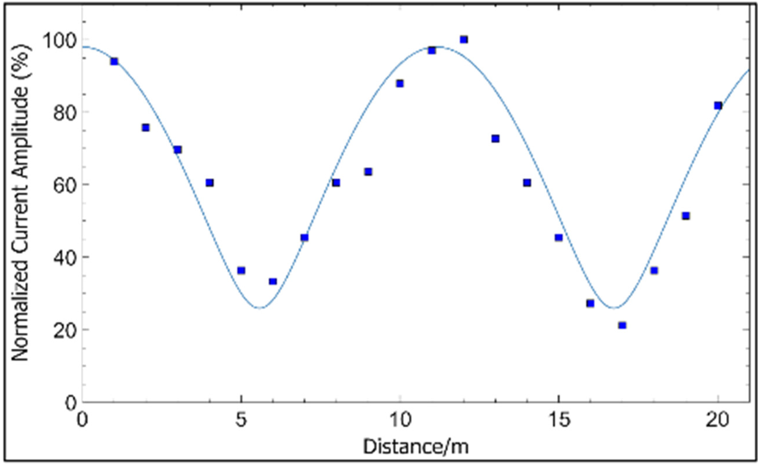
Figure 2 shows the results of these measurements taken every metre along the loop, and it shows a clear stationary wave pattern. These results agree with the literature about the current distribution on loop antennas, the theory of which is close to the one here considered.
The difference between the maximum (100%) and minimum (21%) current amplitude levels from the measurements represents 13.55 dB, which can be managed easily by an automatic gain control (AGC) within receptors. There are two possibilities for fully exploiting the advantages of a resonant loop for communications avoiding significant differences in the signal levels along the loop: (I) Find a simple way to excite only the travelling wave mode over a one-wavelength ring (optimal). (II) Work at carrier frequencies low enough in a fashion that the loop length is a fraction of ¼ of the wavelength or less. This is the slower option, but it still leads to carrier frequencies over 2 MHz (assuming a propagation speed of 0.6 c and a loop length of 20 m), significantly higher than the average previously reported.
Regarding solution I, some authors have faced the theory of travelling wave solutions for loop antennas [18], compared with standing wave solutions [19], and even have determined the necessary conditions for exciting the travelling wave modes [11]. All this work, however, is focused on antenna design and consequently looks for the best radiation properties. For our application, radiation losses are not desired, since they mean power losses and could affect the electromagnetic compatibility of the system. Fortunately, the drastic reduction in the loop area due to the particular shape of our setup will prevent the system from great radiation losses, since radiation integrals obtain contributions of opposite current elements much closer to each other [20]. The travelling wave or quasitravelling wave mode of propagation for our system could be achieved by fulfilling some of the conditions exposed in [18,21].
However, these conditions are not easily applicable in a practical environment, so the insertion in series of a nonreciprocal device is proposed. These kinds of devices will attenuate the waves travelling in one direction, leaving unaffected ones travelling in the opposite direction, leading to a travelling wave propagation mode. Some of the possible practical devices that could accomplish this task are magnetic-circulator-based isolators or unity gain amplifiers referenced to Earth in such a way that waves arriving towards the output will find very low impedances to Earth, being attenuated, but the ones arriving towards the input will find very high impedances and will progress to the output almost unaffected. In this work, we focus on resonance control, and isolator insertion is left for future research.
Regarding solution II, if we work at wavelengths four times the length of the loop or bigger, the phase changes along the loop in π /4 radians maximum. For a loop length of ¼ wavelength, the general solution for its current wave is:
A = 1 + J   2   ,   B = 1 J   2   ,   I ( x ) = I ( A e j k x + B e j k x )
where kx goes from 0 to π /2 along the loop length, so the maximum change in the current wave amplitude is:
I m a x I m i n = 2   ,   I m a x I m i n = 1.5   dB
This value is small enough to avoid AGC systems in receptors and simplifies the electronics, allowing carrier frequencies over 2 MHz as explained before. This carrier (depending on the modulation system) can lead to baud rates around 200 kbps, which are higher than the previous baud rates reported in the literature for PLC within PV plants, so even when this mode of propagation represents the lower baud rate for our model, it still supposedly should provide an improvement on the speeds previously reported.
In addition, the resonance condition can still be achieved for this case because even when the impedance variations related to auto interference are almost not present, there is an inductance associated with the line and reactive impedances representing the transceivers (capacitive or inductive depending on the coupling chosen) that must be compensated for with a lumped element in order to push the loop to resonance. For the higher-frequency (lower-wavelength) option, as a starting point, we can consider a model of signal propagation along a closed loop similar to the ones previously mentioned regarding loop antennas, which show series resonances (impedance close to zero) at frequencies whose wavelengths are integer fractions of the loop lengths [20]. In this way, a constructive interference gives rise to a spatial resonance, and a maximum in the signal amplitude is observed. Since one key goal of a communications system is the integrity of the signal, we must satisfy the above condition in our cable loop in order to work at an optimal point with the best SNR possible.
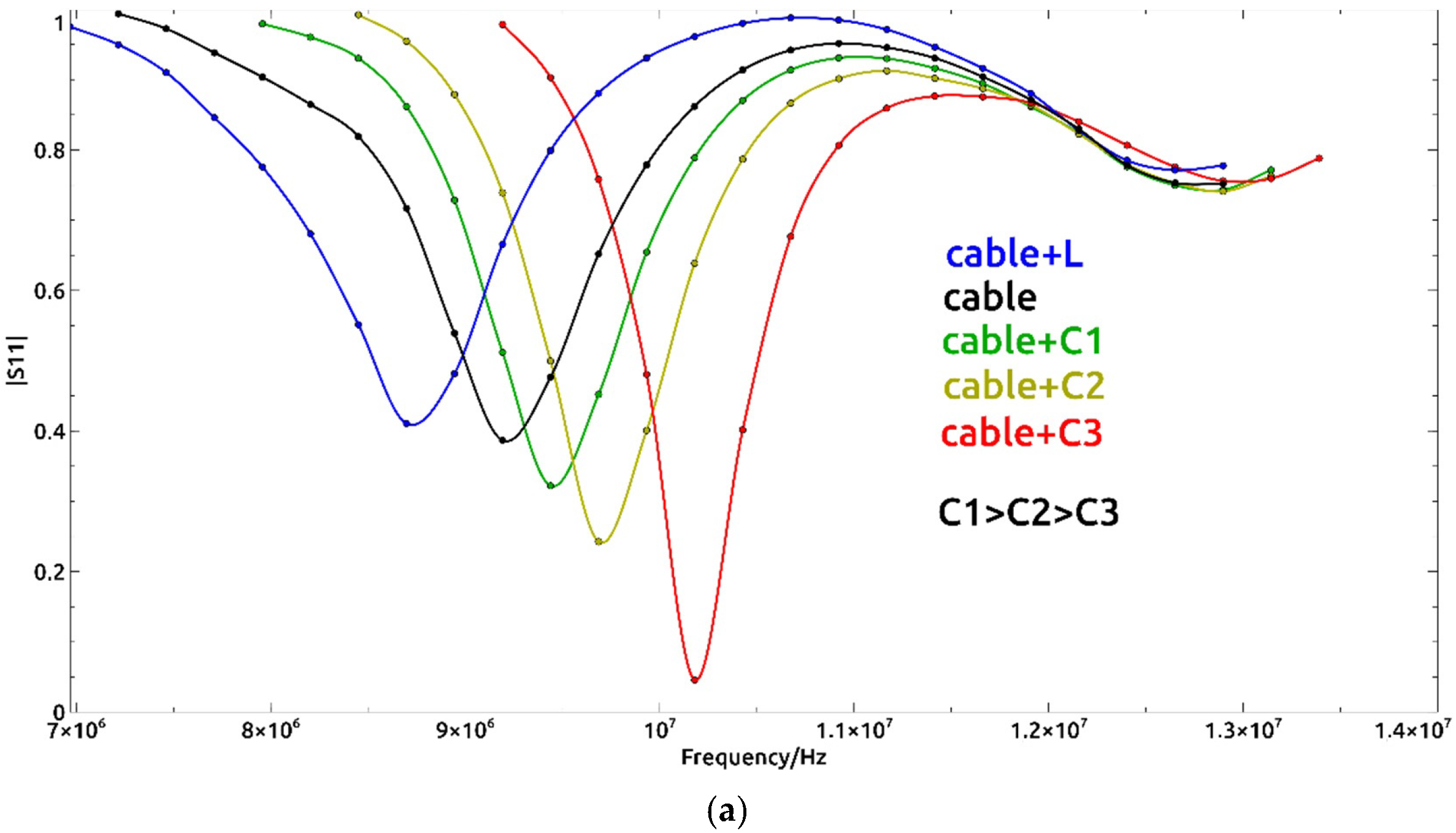
For a chosen carrier frequency, a loop length is fixed to fulfil the above condition; however, the length of the loop is an imposed parameter depending on the physical dimensions of the installation, and therefore it is necessary to find a way to adjust the natural loop resonance to match the frequency of the carrier. The insertion of a coil in series with the cable loop has the effect of increasing the electrical length seen by the signal (length expressed as a wavelength multiple), that is to say, the loop will resonate at lower frequencies. The opposite of this behaviour is seen with the insertion of a capacitor. As such, the insertion of a reactive component in series with the loop could be used to perform the matching between the carrier and loop resonance frequencies. This effect is shown in Figure 3 from our measurements over a typical PV string cable loop 20 m long with a vector network analyser (VNA) connected to the loop, where the resonance condition is recognized by the minimum in the modulus of the S11 scattering parameter (maximum power sent to the loop) and a sudden change in its phase. Figure 3 shows curves around the first resonance frequency (9.192 MHz without compensation) corresponding to the connection in series of a coil, three values of capacitors and the raw cable.
These measurements have been used to determine more precisely the phase velocity in our PV cable. Since the first cable resonance (9.192 MHz) corresponds to one wavelength in the 20 m long cable:
λ = V f f V f = 20 m x f = 20 9192000 = 0.613 c

2.2. Materials

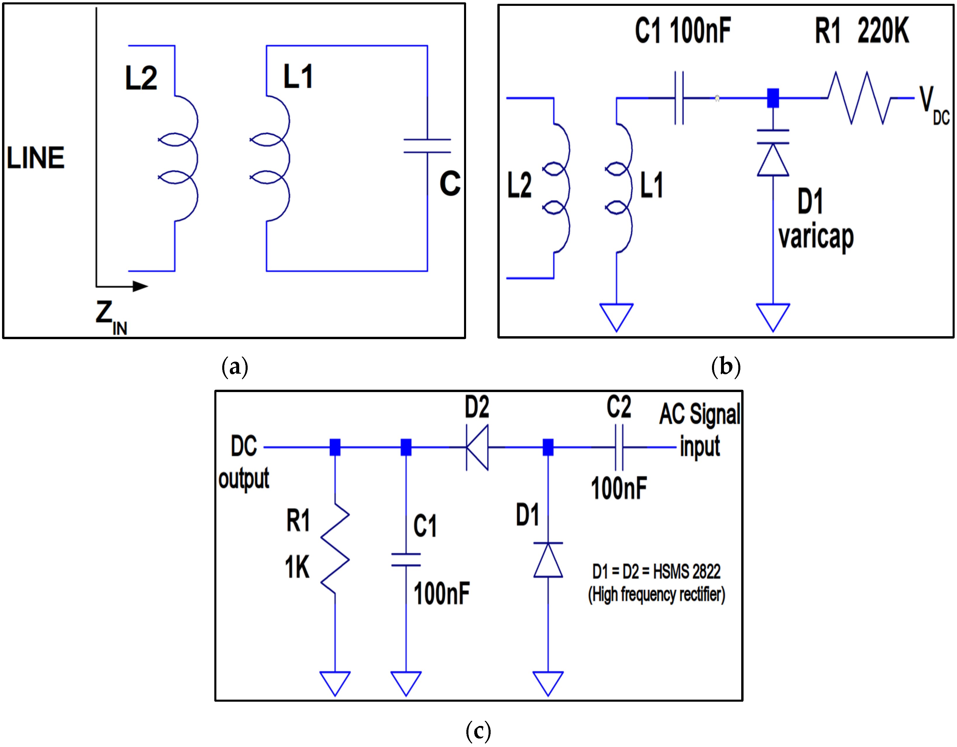
Even though a preinstallation length compensation is feasible (installing a fixed reactive series component), employing automatic adjustable tuning would more so be convenient in confining the transmission around an optimal point, in order to account for the inevitable occurrence of small variations in the loop (for example, the addition of one more PV module to a string, which would increase the loop physical length). For this purpose, a simple tuning circuit was designed which was able to show either capacitive or inductive impedance by means of a control voltage. The basic variable component used was a varicap diode whose capacity could be adjusted depending on the inverse voltage applied. The circuit is shown in Figure 4a, and it is composed of a toroidal transformer with the primary (L2) connected to the cable loop and the secondary (L1) connected to the variable capacitor (C) (voltage controlled). The actual implementation circuit for the voltage-controlled capacitor is shown in Figure 4b.
The network analysis of the circuit in Figure 4a leads to an impedance seen from the primary port:
Z = j w L 2 ( 1 w 2   L 1 C   ( 1 K 2 ) ) ÷ ( 1 w 2 L 1 C )
where the mutual inductance coefficient in the transformer is expressed by:
M = K L 1 L 2
and K is the coupling coefficient, showing a parallel resonance at
w 1 = 1 ÷ L 1 C
and a series resonance at
w 2 = w 1 ÷ 1 K 2
This impedance has two inductive regions, ( w < w 1 ) and ( w > w 2 ) , and one capacitive region: ( w 1 < w < w 2 ) . In the centre of the capacitive region with a good coupling in the transformer ( 1 K 2 < < 1 ) , we have ( 1 > > w 2   L 1 C   ( 1 K 2 ) and ( 1 < < w 2 L 1 C ) , so
Z   1 ÷ ( j w C L 1 L 2 )
and our circuit works as a capacitor multiplier by the factor L 1 L 2 , which can be very useful for loops requiring high-capacitive compensation with values higher than the maximum achieved by the varicap diode, for example, for loops with high inductance in series (the inductive coupling of the transceivers).
For loops with low series inductance (the capacitive coupling of transceivers), the usual length of a typical PV string and carrier frequencies over 5 MHz, our circuit is better used in the region around the higher frequency of resonance w 2 , where the impedance is close to zero, and for frequencies lower than w 2 the impedance is capacitive, and for frequencies higher than w 2 the impedance is inductive. Around this region and ( 1 w 2 L 1 C ) , the impedance can be expressed as:
Z = j w L 2 ( 1 K 2 ) j L 2 ÷ ( w L 1 C )
equivalent to a series LC circuit with
L e q u = L 2 ( 1 K 2 )
and
C e q u = L 1 L 2 C
resonant at w 2 . Since the capacitor C can be dynamically adjusted, connecting this circuit in series with the cable loop, we can add series inductance, capacitance or none of them depending on what is required by the loop, and the dynamic adjusting range can be selected with the value of L 2 since it is a common factor in the expression of Z around w 2 . The possibility of the capacitance control varying a biasing inverse voltage on the varicap diode allows us to implement a microcontroller-based tuning system that will also require some kind of detection of the resonance condition in the loop.
The carrier amplitude through the primary coil in the circuit in Figure 4a will show a maximum if the loop is pushed to resonance, so if this signal is used as an input for a voltage doubler detection circuit (Figure 4c), we will obtain at the output a DC voltage proportional to the amplitude of the carrier in the loop and the resonance can be detected as a maximum in the DC voltage output. Finally, automatic resonance adjusting can be implemented by sampling the detector DC output with an analogue-to-digital converter (ADC) integrated in the microcontroller (MCU), where the convenient firmware will search for a maximum outputting a DC voltage sweep towards the tuning circuit.
Figure 5 shows the real implementation of the circuits proposed, with all the components labelled. Figure 5a shows the front side of the board and Figure 5b shows the back side.
The PV plant used is shown in Figure 6. This plant is located on the facilities of the Duques de Soria campus of the University of Valladolid. The campus is in the city of Soria, Spain. The modules used in this article for the communication line are those on the upper row. Each module has the characteristics shown in Table 1.

3. Results

Figure 7 shows the action of the compensation described, where a 20-m-long loop was kept in resonance at 9.5 MHz initially with the corresponding control voltage of 5 V. Then, the length of the loop was shortened to 15.10 m, and with the resonance control electronics off, the resonance frequency was displaced to 11.1 MHz. If we then switched on the electronics, the control voltage was readjusted by the MCU to get the resonance back to 9.5 MHz. All the electronics described above could work to keep the resonance condition on any of the two modes described in Section 2. The S21 modulus was measured with a VNA connected in series with the loop, the tuning circuit and a 50-ohm load. Maximums show the frequencies of minimal attenuation of the propagation along the (loop)-(tuning circuit) chain. The black trace corresponds to the 20 m cable with a control voltage of 5 V in the tuning circuit, where the maximum is over the chosen carrier frequency (9.5 MHz). The blue solid trace corresponds to a variation in the loop length from 20.00 m to 15.10 m with no change in control voltage, and the new maximum is over 11.1 MHz and the carrier (9.5 MHz) is attenuated from |S21| = 0.228 to 0.100. The blue dashed trace corresponds to the new loop length (15.10 m) after the tuning circuit action for compensation, leading to a control voltage of 0.9 V, and the maximum is back over the carrier at 9.5 MHz.
During the current distribution measurements in the one-wavelength loop presented before (Figure 2), with an exciting signal of 10 volts in amplitude, the absolute voltages measured across the current sensor were between 70 and 330 mV, which, considering that the sensor sensibility is 10 Volts/Amp, indicates averaged current amplitude values in the order of 200 mA. This suggests that with much lower exciting voltages, communication with reasonable SNRs is possible due to loop resonance, making simpler and low-cost transceivers conceivable.
As a validation of the current levels present in the short-loop configuration (¼ wavelength), measurements were made over an experimental setup composed of a cable loop 20 m long with ten capacitors and ten small toroidal transformers distributed evenly in series simulating the bypass capacitors and the transceiver inductively coupled and installed within each PV module in a real installation. The toroidal transformers had a transformation ratio of 30:1 with the secondary connected to the loop, and their inductances were adjusted to form with the bypass capacitors LC resonators at the carrier frequency, in such a way that the transceivers were LC resonators at the same frequency as the loop resonance. The control electronics were also placed in series with the loop. A carrier frequency of 1 MHz was chosen, fulfilling the condition of a loop shorter than ¼ wavelength, and was injected in the primary of one of the transformers with an amplitude of 5 volts, simulating a transmission from one of the transceivers towards the others. The voltage amplitude measurements at the primaries of the ten transformers receiving the signal are shown in Table 2.

4. Conclusions and Future Works

An analysis of a ring topology as physical support for a PLC system specially intended for PV strings has been presented, proposing that pushing this loop to resonance optimises the reception levels along the cable. Previous works on this subject had proposed resonant circuits for coupling to the line; we added here to this feature the possibility of working with the whole loop under resonance, improving even more the signal levels along the line. In addition, the conditions needed for the levels to be reasonably equalised has been derived. Control electronics have been designed to keep the communications signal path on resonance, making the system flexible and able to self-adapt to different specific installations or changes within the same setup. As this check and adaptation to resonance is a task that does not need to be accomplished continuously (it would be enough to execute it once per day), the MCU that controls all the communications in a final application could be the same, allowing a lower-cost system.
The insertion of transmission (TX) and reception (RX) circuits along the loop shows reactive impedances (inductive or capacitive coupled to the line) or even small resistances, consequently modifying the resonance condition on the loop; nonetheless, our tests have shown that the addition of the compensation reactance supplied by the circuit described before is able to return the loop to the optimal working point of resonance. The approach here presented is useful as a starting point for further research that could determine the precise influence of lumped impedances along the loop in the communications performance, but for moderate reactances in the TX/RX circuits (enough for signal injection and recovery), the compensation circuit is enough, with only small deviations compared to the behaviour of the raw cable loop.
Two options regarding the relationship between the loop length and the wavelength have been presented: a loop with one wavelength perimeter and a loop with ¼ wavelength perimeter or less. The measurement levels in the loop have shown the possibility of working with relatively low signal levels without compromising the SNR in both options, allowing the design of cheaper and simpler transceivers. The main line of research from our results must be to explore and test for future work the ways proposed to excite the travelling wave mode in the one wavelength loop, which in essence could suppose a great leap forward for equalising the signal levels working at carrier frequencies over 5 MHz, leading to baud rates close to or even over 1 Mbps (depending on the spectral efficiency of the modulation scheme chosen), keeping all the advantages of working in resonance.

Author Contributions

Conceptualisation, J.I.M.-A. and L.H.-C.; methodology, J.I.M.-A., V.A.G., M.S.M.W. and L.H.-C.; validation, J.I.M.-A., V.A.G., M.S.M.W., J.G.F.C. and L.H.-C.; formal analysis, J.I.M.-A. and M.S.M.W.; investigation, J.I.M.-A., V.A.G., M.S.M.W., A.R.-P., D.F.-M., F.J.S.-P. and L.H.-C.; writing—original draft preparation, J.I.M.-A., M.S.M.W., S.G.-S. and L.H.-C.; writing—review and editing, J.I.M.-A., J.G.F.C., S.G.-S. and M.S.M.W.; supervision, L.H.-C.; project administration, L.H.-C.; funding acquisition, J.I.M.-A. and L.H.-C. All authors have read and agreed to the published version of the manuscript.

Funding

This study was supported by the Universidad of Valladolid with the predoctoral contracts of 2020 cofunded by Santander Bank. This study was supported by the Universidad of Valladolid with ERASMUS+ KA-107.

Institutional Review Board Statement

Not applicable.

Informed Consent Statement

Not applicable.

Data Availability Statement

Not applicable.

Conflicts of Interest

The authors declare no conflict of interest.

References

  1. Morales-Aragonés, J.I.; Gallardo-Saavedra, S.; Alonso-Gómez, V.; Sánchez-Pacheco, F.J.; González, M.A.; Martínez, O.; Muñoz-García, M.A.; Alonso-García, M.D.C.; Hernández-Callejo, L. Low-Cost Electronics for Online I-V Tracing at Photovoltaic Module Level: Development of Two Strategies and Comparison between Them. Electronics 2021, 10, 671. [Google Scholar] [CrossRef]
  2. Kurniawan, A.; Taqwa, A.; Bow, Y. PLC Application as an Automatic Transfer Switch for on-grid PV System; Case Study Jakabaring Solar Power Plant Palembang. J. Phys. Conf. Ser. 2019, 1167, 012026. [Google Scholar] [CrossRef]
  3. Kabalci, E.; Kabalci, Y. A measurement and power line communication system design for renewable smart grids. Meas. Sci. Rev. 2013, 13, 248–252. [Google Scholar] [CrossRef]
  4. Ropp, M.E.; Aaker, K.; Haigh, J.; Sabbah, N. Using power line carrier communications to prevent islanding. In Proceedings of the Name of the Conference Record of the Twenty-Eighth IEEE Photovoltaic Specialists Conference-2000 (Cat. No. 00CH37036), Anchorage, AK, USA, 15–22 September 2000; pp. 1675–1678. [Google Scholar] [CrossRef]
  5. Evans, D.; Cox, R. Powerline communications strategy enabling fully decentralized control of AC-stacked PV inverters. In Proceedings of the 2017 IEEE Energy Conversion Congress and Exposition (ECCE), Cincinnati, OH, USA, 1–5 October 2017; pp. 2277–2284. [Google Scholar] [CrossRef]
  6. Han, J.; Choi, C.S.; Park, W.K.; Lee, I.; Kim, S.H. PLC-based photovoltaic system management for smart home energy management system. IEEE Trans. Consum. Electron. 2014, 60, 184–189. [Google Scholar] [CrossRef]
  7. Jonke, P.; Eder, C.; Stockl, J.; Schwark, M. Development of a module integrated photovoltaic monitoring system. In Proceedings of the IECON 2013-39th Annual Conference of the IEEE Industrial Electronics Society, Vienna, Austria, 10–13 November 2013; pp. 8080–8084. [Google Scholar]
  8. Mao, W.; Zhang, X.; Cao, R.; Wang, F.; Zhao, T.; Xu, L. A research on power line communication based on parallel resonant coupling technology in pv module monitoring. IEEE Trans. Ind. Electron. 2018, 65, 2653–2662. [Google Scholar] [CrossRef]
  9. Goubau, G. Surface Waves and Their Application to Transmission Lines. J. Appl. Phys. 2004, 21, 1119. [Google Scholar] [CrossRef]
  10. Sommerfeld, A. Ueber die Fortpflanzung elektrodynamischer Wellen längs eines Drahtes. Ann. Phys. 1899, 303, 233–290. [Google Scholar] [CrossRef] [Green Version]
  11. US8497749B2-Single Conductor Surface Wave Transmission Line System for Terminating E Field Lines at Points Along the Single Conductor-Google Patents. Available online: https://patents.google.com/patent/US8497749B2/en (accessed on 28 July 2022).
  12. Roberts, T.E. Theory of the Single-Wire Transmission Line. J. Appl. Phys. 2004, 24, 57. [Google Scholar] [CrossRef]
  13. Vaughn, B.; Peroulis, D. An updated applied formulation for the Goubau transmission line. J. Appl. Phys. 2019, 126, 194902. [Google Scholar] [CrossRef]
  14. Santos, A.C.F.; Santos, W.S.; Aguiar, C.E. Electromagnetic wave velocities: An experimental approach. Eur. J. Phys. 2013, 34, 591–597. [Google Scholar] [CrossRef]
  15. Sanchez-Pacheco, F.J.; Sotorrio-Ruiz, P.J.; Heredia-Larrubia, J.R.; Perez-Hidalgo, F.; de Cardona, M.S. PLC-Based PV Plants Smart Monitoring System: Field Measurements and Uncertainty Estimation. IEEE Trans. Instrum. Meas. 2014, 63, 2215–2222. [Google Scholar] [CrossRef]
  16. Han, J.; Lee, I.; Kim, S.H. User-friendly monitoring system for residential PV system based on low-cost power line communication. IEEE Trans. Consum. Electron. 2015, 61, 175–180. [Google Scholar] [CrossRef]
  17. Ochiai, H.; Ikegami, H. PPLC-PV: A pulse power line communication for series-connected PV monitoring. In Proceedings of the 2016 IEEE International Conference on Smart Grid Communications, SmartGridComm 2016, Sydney, Australia, 6–9 November 2016; pp. 338–344. [Google Scholar]
  18. Chen, K.M.; King, R.W.P. A loop antenna coupled to a four-wire line and its possible use as an element in a circularly polarized end-fire array. Proc. IEE Part C Monogr. 1962, 109, 55. [Google Scholar] [CrossRef]
  19. Adekola, S.A. On the excitation of a circular loop antenna by travelling-and standing-wave current distributions. Int. J. Electron. 1983, 54, 705–732. [Google Scholar] [CrossRef]
  20. Boswell, A. Loop antennas in the 3-30 MHz band. In Proceedings of the 8th International Conference on High-Frequency Radio Systems and Techniques, Guildford, UK, 10–13 July 2000; pp. 33–36. [Google Scholar]
  21. Li, R.; Bushyager, N.A.; Laskar, J.; Tentzeris, M.M. Determination of reactance loading for circularly polarized circular loop antennas with a uniform traveling-wave current distribution. IEEE Trans. Antennas Propag. 2005, 53, 3920–3929. [Google Scholar] [CrossRef] [Green Version]
Figure 1. Schematic of the communications loop (signal path) excited by a current generator (I), with a perimeter d.
Applsci 12 07973 g001
Figure 2. Current amplitude distribution along the loop (normalised (%); measurement points and fitting to a stationary wave envelope function).
Applsci 12 07973 g002
Figure 3. The shift of the loop resonance frequency with the addition of a reactance in series: the modulus (a) and phase (b) of the scattering parameter-1 measured with a VNA connected to the raw cable loop and with the addition in series of a coil and three increasing values of capacitors.
Applsci 12 07973 g003aApplsci 12 07973 g003b
Figure 4. Schematic of tuning circuit in (a) its generic representation and (b) actual implementation, and (c) schematic of voltage doubler detection circuit.
Applsci 12 07973 g004
Figure 5. Picture of the electronics developed for loop automatic tuning: (a) front side; (b) back side.
Applsci 12 07973 g005
Figure 6. PV plant on Duques de Soria campus of the University of Valladolid.
Applsci 12 07973 g006
Figure 7. Effect of microcontroller action to retune the loop, in response to variations in cable distance.
Applsci 12 07973 g007
Table 1. Technical characteristics of the PV module.
ModelCellsPower/WVOC/VISC/AVMPP/VIMPP/A
Eoply72 cells 17544.355.4536.264.83
Table 2. Voltage amplitude measurements of the ¼ wavelength configuration.
ReceiverVoltage Amplitude (V)
132.3
232.1
332.3
433.5
534.6
634.0
733.5
832.7
932.5
1032.8
Publisher’s Note: MDPI stays neutral with regard to jurisdictional claims in published maps and institutional affiliations.

