1. Introduction
There are several methods for evaluating the integrity of materials, and an important category of them is nondestructive evaluation (NDE) or nondestructive testing (NDT) methods. This field includes identifying and characterization the flaw on the surface and under the surface of materials without cutting apart or altering the material [
1]. It means NDT refers to the process of evaluating and inspecting materials to identify or detect defects in comparison with some standards without changing the main features or damage to the tested object. NDT techniques supply affordable ways of assessing a specimen individually or may be applied to the whole material for testing in a manufacturing system for quality control purposes [
2].
There are some advantages and disadvantages inherent to all NDT methods that made them more or less suitable for a particular application in relation to the coverage area, the penetration depth and the problems associated with the interpretation of the results [
3]. For instance, ultrasound testing is a mature technique allowing the identification and characterization of deep defects, but requires contact with the object being inspected and the use of water-based couplants (liquid or gel). Radiography testing provides high-resolution images and deep penetration, but requires access to both sides of the object and employs ionizing radiation, which constitutes a risk of radiation exposure. Infrared thermography testing allows the inspection of large areas in a fast and contactless manner, but is limited to relatively shallow defects and requires advanced signal/image processing for defect characterization. Eddy current testing (ECT) is effective for certain types of defects (cracks, corrosion, etc.) under several layers of materials, but is limited to conductive materials and is not well suited for the detection of delaminations in composites. It has recently been shown that an alternative electromagnetic method based on a capacitive sensor can be used as an NDT method [
2].
For nonconducting materials, NDT methods are not as well developed as compared to those for metallic materials. One approach to evaluate nonconducting materials is to characterize their dielectric properties. The dielectric strength and the dielectric constant are the dielectric properties of nonconducting or low conductivity materials. The voltage that a material can withstand before an electrical breakdown happens is called “dielectric strength” and a measure of the material’s capability of storing electric energy is called “dielectric constant” or “permittivity”.There exist alternative approaches that are based on the characterization of materials permittivity such as microwave techniques and resonant testing. However, these techniques require expensive equipment and/or complex operating procedures. Capacitive sensing on the contrary is a straightforward and inexpensive approach [
2].
The coplanar capacitive technique was first introduced in 2006 [
4]. This novel approach, usually referred to as Capacitive Imaging (CI), is an electromagnetic NDT method that uses arrays of electrodes to generate an electric field distribution within the specimen. The electric field distribution can penetrate within dielectric materials and changes in response to the structure of the material under test leading to a variation in the output voltage [
5,
6]. The capacitive technique has shown great potential to inspect a wide range of materials and structures from insulators to conductors [
5].
CI technique offers a possible way to overcome some of the restrictions imposed by existing NDT methods. For instance, the technique works in a volume averaging manner and therefore the scattering issue with the ultrasonic method is absent [
7]. The affordable cost, straightforward response, noninvasive, no ionizing radiation involved and flexibility in the design of the electrodes provide CI with a great potential to be applied in a extensive range of applications. Furthermore, the coplanar structure allows one-sided inspection [
8], which is especially useful when access to both sides of the specimen is limited [
9]. Moreover, this is a noncontact method [
5] and the liftoff (the air gap between the surface of the electrodes and specimen) can be optimized, leading to an applicable method in the detection of corrosion under insulation (CUI), including the detection of large surface features in metals and therefore the presence of even small amounts of rust [
10]. This technique is especially useful in defence where composites are extensively used for both equipment and strengthening structures [
11]. These features of coplanar capacitive sensor make it an attractive option for applications in NDT [
6], material characterization [
8], and imaging [
12].
The principle of this technique involves placing two (or more) electrodes over the surface of the sample and then applying an AC voltage between them. This system acts as a capacitor whose altering in capacitance indicates variations in the internal structure (such as the presence of a defect) [
13]. Normally, in a regular capacitor, the plates are parallel. When a voltage is applied between these plates, they produce a uniform electric field distribution. This electric field does not restrict itself to the area between the electrodes when the electrodes are gradually open, but extends to a wider space and forms a fringing field [
9]. This field expands into the specimen for NDT. Scanning a set of electrodes over the surface of the sample and measuring variations in stored charges for a given voltage creates a map of the changes in the electrical properties within the specimen [
7]. The fringing field between the driving and sensing electrodes becomes predominant when the electrodes open to a coplanar plane. This kind of sensor is named a coplanar sensor in literature [
9].
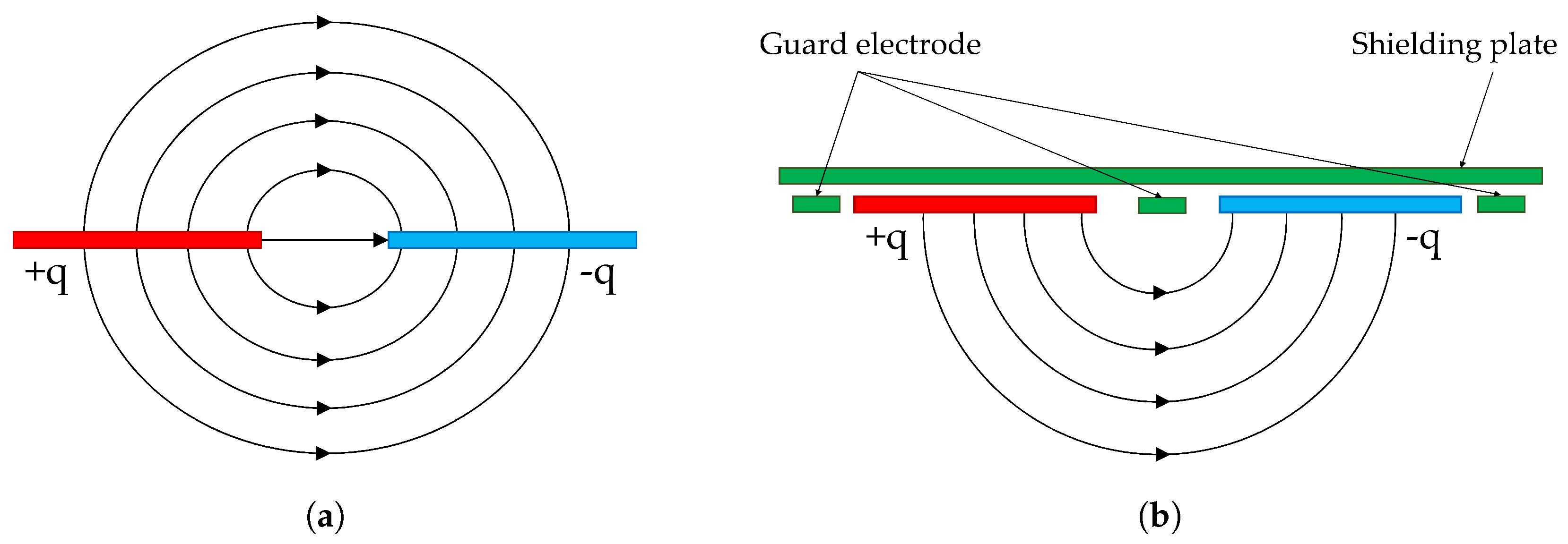
Figure 1 shows a schematic diagram showing how the electric field distribution changes when the two capacitor electrodes change from a parallel-plate to a coplanar so that the final part produces a fringing field [
7]. The coplanar electrodes can be scanned over the surface of a large mechanical structure to investigate the physical properties of the specimen and obtain information.
Such as some other NDT methods, the capacitive technique is sensitive to liftoff, which refers to the air gap between the surface of the coplanar electrodes and specimen which causes a decrease in the capacitance between the electrodes and hence a reduction in output voltage. In addition, it reduces the extent of penetration of the electric field into the sample which leads to a decrease in the depth of penetration [
9]. The lift-ff should therefore be as small as possible to achieve greater signal strength and sensing depth (especially for investigating dielectric material) [
14] with no need to use couplant materials.
The sensor manufacturing steps include material selection for electrodes, the insulation layer of the surface of the electrodes, the sensor substrate, and eventually the selection of a production technique. The electrodes are made of materials with high electrical conductance, such as copper. A thin insulation layer (with a few micrometres in thickness) is usually placed on the surface of the electrode to prevent direct contact of the electrodes with the specimen and to protect the electrode surface against scratches. The thickness of the insulation layer and the sensor substrate influence the electric field strength and depth of penetration, therefore, need to be optimized. Several manufacturing techniques of the capacitive sensor, including microelectromechanical systems (MEMS) [
15], printed circuit boards (PCB) and manual production can be selected depending on sensor dimensions and costs [
9].
To evaluate the sensor performance, it is required to explain the general design parameters. Therefore, in this paper, firstly the design factors such as the geometry of the electrodes, the number of electrodes and their arrangement, shielding plate and guard electrode of the capacitive sensor are presented. The electric field distribution from a coplanar capacitive sensor in the different condition of a specimen, which are the sound sample, the sample with a crack on the surface, and the sample with subsurface defect, was considered by 3D finite element (FE) modeling in COMSOL Multiphysics software. The real sample, a Plexiglas plate with defects at different depths, was simulated using FE modeling and the electric field strength was measured. It was shown that the different depths of the defect have different electric field strength and distribution. These results approved by physical experiments and It was illustrated that the electric field strength and distribution changed with respect to the defect depth in agreement with experimental data.
4. Numerical Simulation and Experimental Work
The capacitive probe is the key part of the instrumentation and requires to be designed carefully. For sensors with a constant overall electrode area, the penetration depth increases with the distance between the electrodes. A larger distance between electrodes will however decrease the signal strength (the measured output) as the coupling between the driving and sensing electrodes would be weaker and would reduce the image resolution as they are sampling a larger area of the sample and more importantly it is physically disallowed if the overall probe size is constant. To balance these trade-offs, triangular-shaped electrodes can be applied [
20]. This electrode geometry is an interesting choice for different defect detection in various material as it would likely allow deep penetration into the specimen, with a symmetrical electric field distribution. As stated in the previous section, the electric field distribution is a function of the electrode geometry and so this aspect has to be designed with care [
5]. The coplanar electrodes with the same overall sensing areas are used in this work, as shown in
Figure 3, namely capacitive probes with back-to-back triangular electrodes. Generally, this pair of triangular electrodes could be specified by the overall size, the base (b), the height (h) of each triangle and the separation distance between the closest points of the two triangles (s). In this work, the triangular electrodes have the same overall size with b = 15.0 mm, h = 15.0 mm and s = 4.0 mm. In addition, a shielding plate and guard electrode are employed for this coplanar capacitive sensor. Note that the field distribution predicted by the finite element (FE) model, as discussed below, is determined primarily by these geometric factors in the model.
4.1. Numerical Simulation
Conceptually, the capacitive method is straightforward. The electrodes provide an electric field distribution when an AC voltage is applied between the driving and sensing electrodes. The presence of the specimen and any variation in its properties (such as the presence of a defect) within the area covered by the electric field will change the field pattern distribution. A distortion in the electric field causes a change in the charge induced in the sensing electrode, and this change in the charge can be used for defect detection purposes [
7]. The resulting signal is sent to standard instruments such as charge amplifiers that increase the signal-to-noise ratio (SNR) and allow small changes in the signal to be recorded, processed and outputted as a DC voltage. Since the presence of delaminations, cracks and other imperfections changes the electric field distribution in various distinctive ways, a basis for detecting defects can be established [
5].
In order to understand the way electric field distributions are produced by the electrodes, and to identify how they may interact with the materials of interest, it was felt important to model the expected behavior. In this paper, we want to demonstrate the distribution of the electric field and how changes in the specimen might affect the output. Finite element (FE) modeling enables valuable information (such as visualization of the results) to towards analyzing the performance of the capacitive sensor more easily. Although finite element methods are well established in engineering calculation, care must be taken to secure suitable mesh densities in critical regions, in particular near to the source of field singularities [
21]. The major source of errors is the discretization processes of the conductor segments bordering different dielectrics and of the dielectric interfaces. However, there is no need to do the complicated mathematical process in order to simulate the defects in the samples in the finite element method. This is a useful tool for predicting the fields from capacitive electrodes and how these fields are likely to interact with different materials and defects [
5,
22]. Therefore, finite element (FE) modeling has been employed to predict the distribution of the electric field from capacitive electrodes and signal changes that are likely to be generated under experimental conditions.
Theoretical simulations were conducted using COMSOL™ Multiphysics FE package, and using its AC/DC module, electric currents (ec)-type, which can be used to model the distribution of the electric field in different situations. The purpose of this analysis is to observe the field distribution and the variation of electric field strength as a function of the sample properties such as existing defects and depths of a defect. The electric field distribution for all situations has been analyzed using a three-dimensional (3D) finite element method.
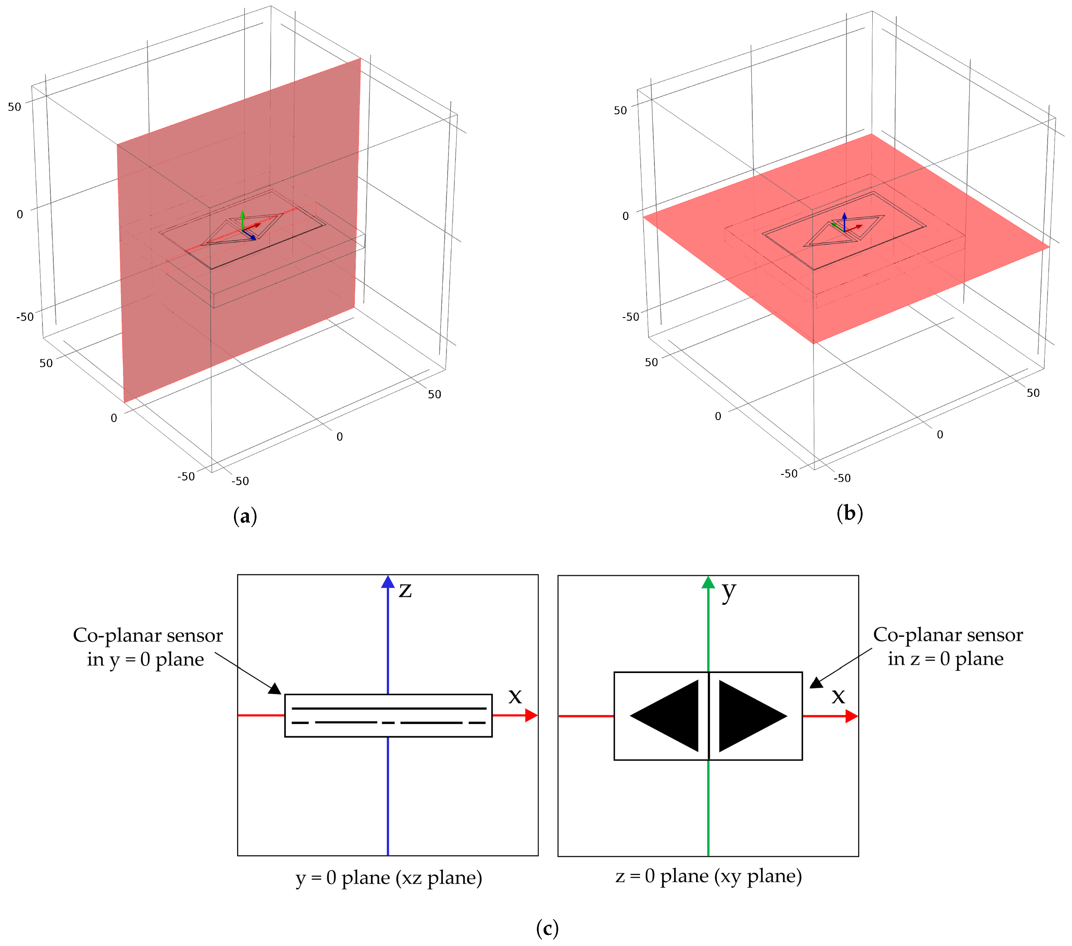
In this model, the driving and sensing electrode were driven by a +5.0 V and −5.0 V, respectively, with a 100 kHz sinusoidal signal. The shielding plate and guard electrode were set to ground potential. Based on this, there is an electric field between the positive and negative electrodes and the electric field distribution is formed in the local region in the specimen under the electrode pair and the liftoff between the sample and probe. A pair of a coplanar triangular electrode is placed above the surface of a specimen with 1.0 mm liftoff, and the setup is enclosed in a 120 mm × 120 mm × 120 mm block centred at the point (
x = 0,
y = 0,
z = 0). This block was a zero-charge boundary airbox and defined to be the computational domain, as shown in
Figure 4a. A physics-controlled mesh was used and the mesh generation density is set to “Finer”. Providing the environment and necessary system parameters the mesh is generated in the model as shown in
Figure 4b.
Figure 4c shows the solved back-to-back triangular capacitive sensor model for a sound specimen. The contour lines on top of the specimen represent electric potential values.
In the coordinate system illustrated in
Figure 5, based on which the results will be shown henceforth, the surface of the electrodes is centred at (
y = 0 or
z = 0).
Y = 0 plane (or
xz plane) is the cross-sectional plane along the long axis of symmetry of the capacitive sensor, as shown in
Figure 5a, and
z = 0 plane (or
xy plane) is the parallel plane under the probe surface at the sample surface, as shown in
Figure 5b. To clarify the results, the plane coordinate systems for the two types of cross-sections are presented in
Figure 5c.
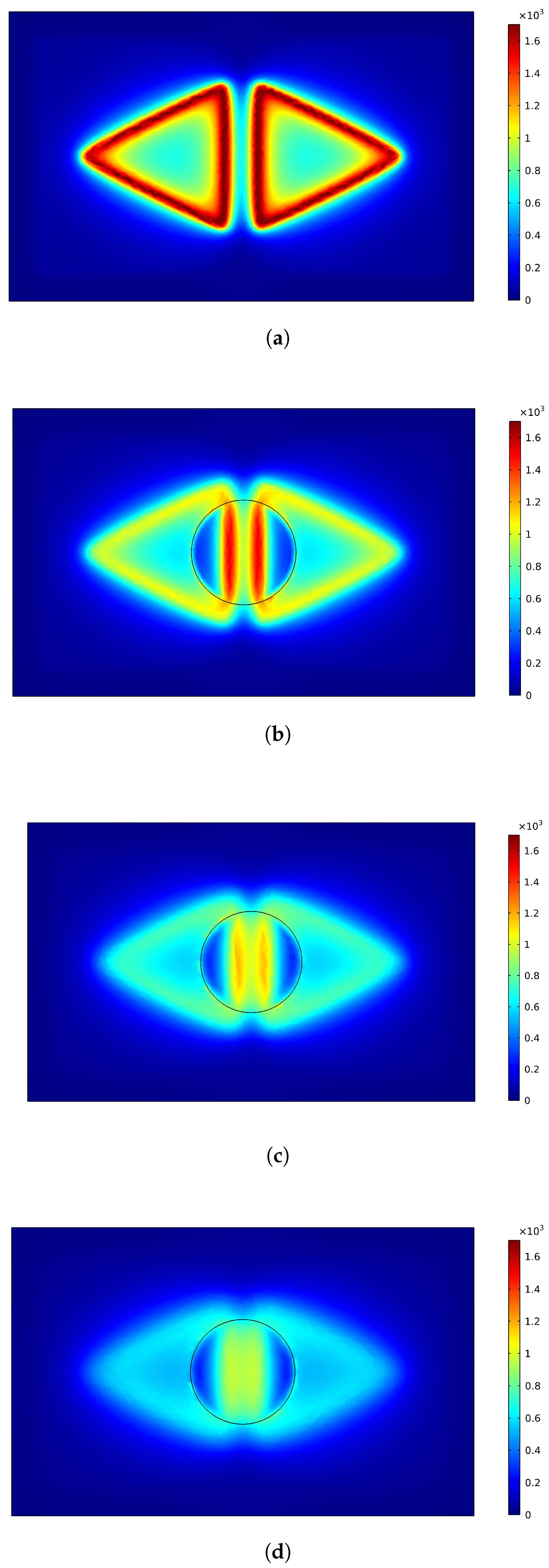
Figure 6 shows a sample of the electric field distribution prediction of the 3D finite element models for the coplanar capacitive electrodes and how these fields behave under different conditions. This figure is a contour plot of the electric field in the
y = 0 plane.
Figure 6a shows this example for a sound zone of a specimen,
Figure 6b shows a sample of output for a defective zone filled with air, and
Figure 6c shows the electric field distribution for a specimen with a narrow crack on the surface. It can be seen that the presence of defects distorts the electric field within and around the regions of discontinuity in the sample and this leads to a variation in the detectable signal on the sensing electrode. This is because of the different dielectric properties such as permittivity (or dielectric constant) presumed for the sample and defects. Therefore, the model shows how the capacitive sensor detects the defects due to the different dielectric properties between the sample and defect.
Simulations were conducted to determine the effect of various depths of subsurface defects on the electric field strength. The real nonconducting sample, a Plexiglas plate containing three subsurface air-filled cylindrical voids at different depths, was simulated.
Figure 7 shows a surface plot of the electric field of the back-to-back triangular electrodes for the different defect depth in the
z = 0 planes, including
Figure 7a a sound sample, (b) a defect in 0.5 mm depth, (c) a defect in 1.0 mm depth, and (d) a defect in 1.5 mm depth. By comparing the results, it can be inferred the presence of the air-filled defect at different depths causes a different distortion of the electric field and this would lead to a detectable change in the output. This is caused by the different values of permittivity (or dielectric constant) assumed for the solid sample (Plexiglas, permittivity = 3.4) and air (permittivity = 1.0). Thus, the model shows how the capacitive probe detects subsurface defects due to a permittivity difference between the sample and defect.
It is obvious from these results that the electric field strength decreases as the depth of the defect increases. In other words, the penetration depth and strength of the electric field vary for different depths of the defect. This is confirmed by the experimental result to be shown later in this work. Moreover, these figures show that different depths of a defect create a different electric field pattern which can be used to estimate the defect depth.
4.2. Experimental Results
Figure 8 illustrates the experimental arrangement used for the capacitive technique experiments presented in this work. The experiments use a capacitance setup that is composed of a single pair of back-to-back triangular electrodes made of copper plates as shown in
Figure 3. A shielding plate is placed on its top side to ensure that the radiated electric field emanates predominantly in the direction towards the specimen and to provide protection against the effect of the ambient stray fields on the output results. In addition, a guard electrode is applied to increase the penetration depth of the sensor. One of the electrodes is used as a driver electrode and the other one as a receiver. The driving electrode was excited by a sinusoidal voltage of 10 V amplitude peak-to-peak at a frequency of 100 kHz and the shielding plate and guard electrode are connected to the ground potential. To generate an electric field, one of the plates is employed as a transmitter and connected to Ectane. Ectane is a multitechnology, powerful and compact instrument for generating and analyzing signals. The frequency range of this instrument is 5 Hz up to 10 MHz and the generator output is up to 20 V, peak to peak. A differential amplifier is placed inside Ectane to process the received signal successively. The output signal from the Ectane is a simple DC voltage level that is proportional to the instantaneous value of the dielectric property of the material averaged over the field distribution within the material.
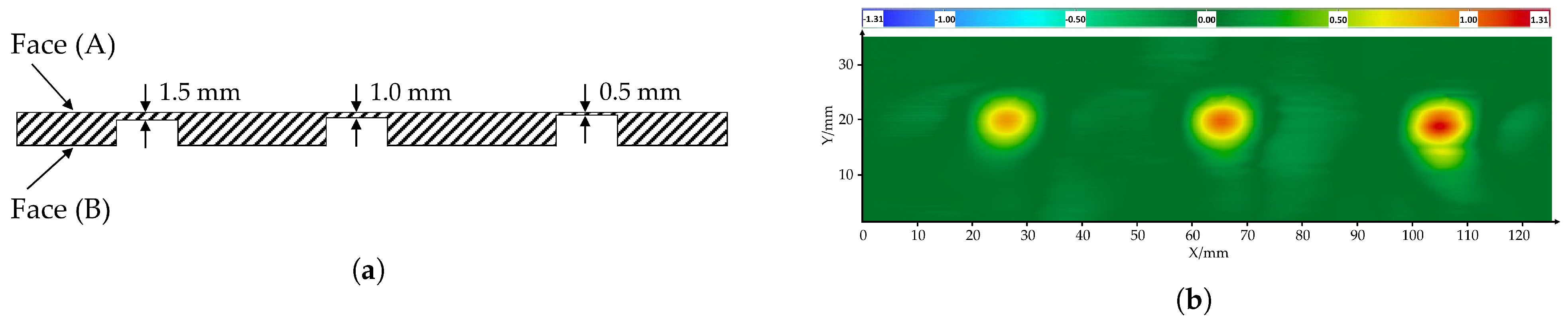
The hidden depth of the defect is also a factor affecting the coplanar capacitive sensor performance. To investigate the effects of it in nonconducting specimens, a set of experiments were carried out on a 6.5 mm thick Plexiglas plate. The plate contains three subsurface defects of 12 mm diameter located at different depths (0.5 mm, 1.0 mm, and 1.5 mm).
Figure 9a illustrates the schematic diagram of the sample. The coplanar CI probe was scanned over the Face (A) (the face without the defects) using a two-axis scanning system (
x-y table). In this scan, the coplanar capacitive sensor was held 1.0 mm off the surface of the specimen (a constant liftoff = 1.0 mm) and scanned over a 40 mm × 160 mm area with a 0.2 mm step in the
x-axis and 1.0 mm in the
y-axis. The speed of the probe was set to 10 mm/s.
Figure 9b is the image obtained by scanning the coplanar capacitive sensor over the surface of the Plexiglas sample. The technique easily detected these defects, and this is due to the different dielectric properties between the material of the specimen (Plexiglas) and the defect (air). It can be seen from the result, the defect at 0.5 mm depth, which is the shallowest defect in the Plexiglas specimen, appeared as a darker colour, especially a darker red colour which is representing the highest output voltage in this result. Likewise, the other two defects appeared as a lighter area, depending on their depth representing lower output voltage values. This result is in good qualitative agreement with the result of the simulations as seen in
Figure 7.
It can be inferred that when a specimen is placed under the coplanar capacitive electrodes, most of the electric field from the sensor penetrates into the specimen and then ends on the sensing electrode. The dielectric properties of the specimen and defects influence the electric field distribution and, hence, on the electric potential of the sensing electrode. Therefore, an existing defect in the specimen will change the electric field pattern, which leads to the changing in the detectable signal of the sensing electrode. It is worth mentioning the depth of penetration is determined mainly by the geometry of the sensor, the electric properties of the specimen, and the liftoff.
5. Conclusions
A feasibility study of the coplanar capacitive sensing technique which has certain advantages for NDT applications was explored through a numerical simulation and experimental tests. Numerical finite element (FE) analysis was conducted to demonstrate the validity of the proposed defect detection technique. The 3D FE modeling has demonstrated that the electric field distribution of a selected electrode pair penetrate into dielectric materials and can be used to detect the presence of defects in the form of air voids and crack. The preliminary investigation into the appliance of capacitive sensing for the detection of hidden holes within the specimen has been successfully shown. Experimental results on the Plexiglas plate containing subsurface holes of various depths gave a sign of the response of the technique. A good qualitative agreement was observed between the experimental and simulations result. The results obtained by the coplanar capacitive method illustrate that the technique is noncontact, noninvasive, and only requires single-sided access to the specimen. The couplant such as gel or water is not required, and there is no need for specific surface preparation. In addition, there are no radiation exposure problems. Therefore, this technique has the potential to be used in many NDT application areas where traditional methods may have difficulty.
In practice, the condition is typically more complicated compared to the sample inspected during this work. Defect specifications will be unknown, and voids could also be poorly defined. Further development of the capacitive sensor is required to meet various practical needs and provide enhanced diagnostic information, e.g. systematic identification and characterization of defects. It should be emphasized that the depth of the penetration is mainly determined by the probe geometry, the electric properties of the specimen and the liftoff distance between the surface of the probe and the specimen, this will be further studied in future work.


 ,
, 


