1. Introduction
SPIDER (Source for the Production of Ions of Deuterium Extracted from Radio-frequency plasma) is the full-scale prototype of the ITER NBI (Neutral Beam Injector) ion source [
1,
2,
3]. In SPIDER beam source, RF inductively coupled plasma drivers are used to produce hydrogen or deuterium plasma, from which negative ions are electrostatically accelerated by means of a series of grids. SPIDER electrical system provides power to the RF drivers for plasma generation and to the system of grids for the extraction and acceleration of the ion beam. Each RF circuit is designed to be isolated from the rest of the electrical system, but parasitic connections provide alternative circulation paths for RF currents, which caused destructive damage of a power supply (ISEG) output filter and introduced large noise in the measurements performed with the beam-source thermocouples. From a preliminary circuit analysis, the main parasitic element providing an alternative low-impedance path for the RF current was identified as a Capacitive Voltage Divider (CVD) installed at the output of each RF generator, used to obtain the output voltage reading. The proposed solution consisted in the replacement of the CVD at the primary side of the RF generator output transformer; this is based on the idea of increasing the impedance seen by the common mode RF currents [
4]. The solution was implemented and tested in SPIDER with good results [
5]. Even though the modification has proven to be effective, the circulation of RF stray currents in SPIDER electrical system pointed out a major issue that was not taken into account in the design phase. A deeper comprehension of the stray currents phenomenon and an adequate modeling tool would enable the possibility to assess this problem and to develop alternative solutions not only in the existing SPIDER and MITICA configurations, but also for alternative RF system layouts, since a major upgrade of the RF power supplies to solid-state amplifiers is programmed for SPIDER and MITICA [
6]. This paper describes further thoughts and discussions on the problematic and the development of a circuital model for the analysis of RF stray currents in SPIDER electrical system. The section devoted to a simplified analysis of the problem starts from the original interpretation [
4], further developing the understanding of the phenomenon. Then, the simulation results obtained from the model are compared to the measurements performed in SPIDER prior to and following the CVD modification and used to validate the hypothesis on RF stray currents generation.
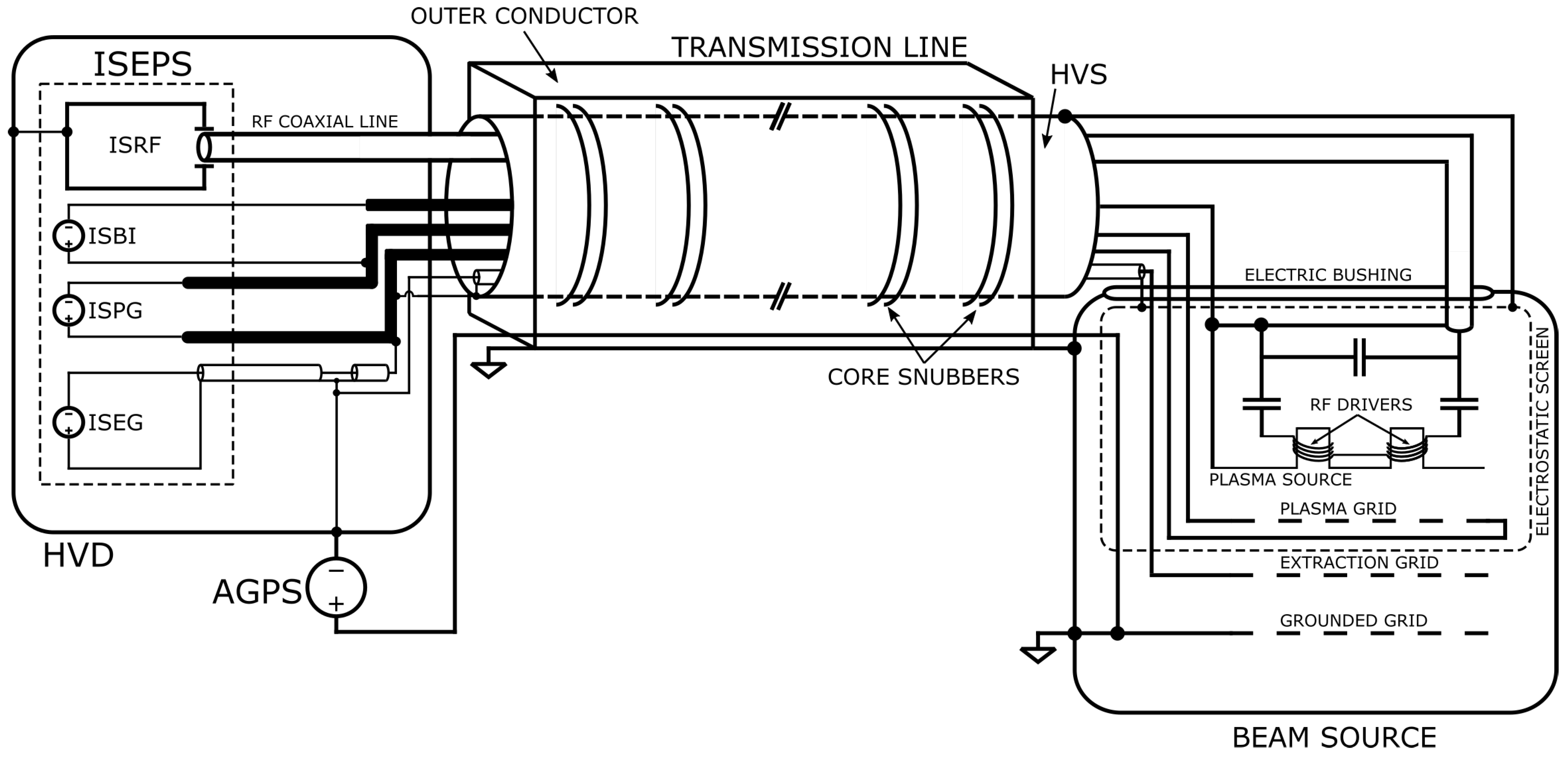
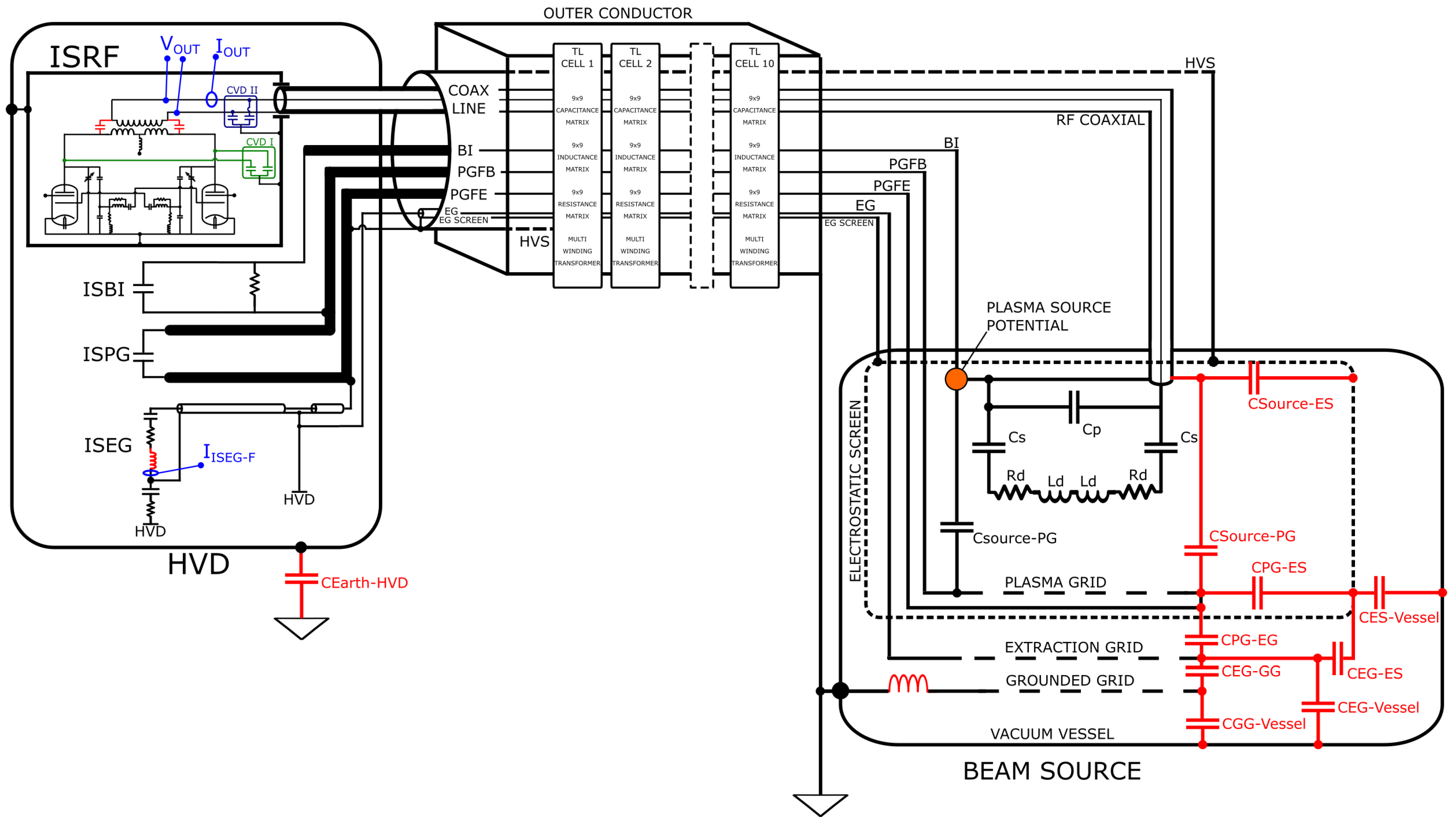
2. Spider Electrical System
For the purpose of this study, it is necessary to consider the electrical connections in the beam source, the arrangement of conductors in the transmission line [
7] and the layout of ISEPS [
8] (Ion Source and Extraction Power Supplies) installed inside the air-insulated HVD, as represented in
Figure 1.
2.1. Beam Source
SPIDER beam source is installed in a vacuum vessel, and it is used to generate and accelerate a beam of negative ions. The components considered in this study are:
RF drivers: eight plasma drivers (two of them shown in
Figure 1) are used to produce hydrogen or deuterium plasma, from which negative ions are extracted and accelerated. The plasma source is divided in four sectors, each consisting of two RF drivers connected in series. Impedance matching is achieved with a capacitive network installed as close as possible to the drivers. In this work, only one sector is considered.
Plasma Grid (PG): the PG produces a magnetic filter field, used to reduce the amount of co-extracted electrons in the ion beam.
Extraction Grid (EG): the EG is used to extract negative ions from the plasma generated by the RF drivers.
Grounded Grid (GG): the GG is the last stage of beam acceleration, and the potential difference between EG and GG represents the beam accelerating voltage.
Electrostatic Screen (ES): an electrostatic screen referred to the PG potential surrounds the beam source to provide a uniform electric field distribution.
2.2. ISEPS and HVD
ISEPS of SPIDER is installed inside the HVD, an air-insulated platform referred to the acceleration potential by means of the Acceleration Grid Power Supply (AGPS), and fed by an insulation transformer. ISEPS power supplies relevant for this study are:
ISRF: four radio-frequency oscillators with a nominal output power of 200 kW on 50 Ω, working in the frequency range 0.9 ÷ 1.1 MHz, supply eight plasma drivers. Each ISRF unit powers two RF drivers. In
Figure 1, only one ISRF unit is represented.
ISBI: the plasma source BIas power supply, rated for 300 V and 600 A.
ISPG: the plasma grid power supply, rated for 15 V and 5 kA.
ISEG: the extraction grid power supply, rated for 12 kV and 140 A.
2.3. Transmission Line
The 23.5 m long (in-axis) multiconductor transmission line transmits the power from ISEPS and AGPS to the beam source. The transmission line is air-insulated, and it is interfaced to the beam source by means of a high-voltage ceramic bushing. The transmission line components considered for this study are:
RF coaxial transmission lines: four rigid 3
inches coaxial lines deliver power from ISRF to the RF drivers in the beam source. The outer conductor of the rf coaxial line is referred to the plasma source potential. Only one RF coaxial line is represented in
Figure 1.
Plasma Grid busbars: two actively cooled busbars are used to transmit power from ISPG to the PG. Depending on their potential reference, they are identified as PGFE (connected to the negative terminal of ISEG in HVD) and PGFB (connected to the positive terminal of ISBI in HVD).
Bias busbar: a busbar is used to connect the beam source to the negative terminal of ISBI in HVD.
Extraction Grid cable: an insulated and screened cable is used to connect the EG to ISEG. The central conductor of the cable, which is connected to the EG, is referred to HVD.
High-Voltage Screen (HVS): all the previous conductors (RF coaxial lines, PG busbars, BI busbar and EG cable) are surrounded by a cylindrical screen, referred to the PG potential.
Distributed Core Snubber (DCS): ten ferromagnetic cores, which envelope the HVS, are installed along the transmission line. They are used to dampen the transients, which develop as a consequence of breakdown between grids.
Outer Conductor: the square-section outer conductor of the transmission line consists of two sandwich copper panels isolated from one another, the inner and outer screens. Their purpose is the minimization of Electromagnetic Interference (EMI) generated in the surrounding environment during breakdown between grids. In
Figure 1, for simplicity, only the outer screen, referred to the beam source, and its connections are represented.
3. Circuital Model
Starting from the electrical model developed for the breakdown analysis of SPIDER [
9,
10,
11], a lighter version focused on the most relevant aspects for the study of RF stray currents was developed in MATLAB Simulink
®. The AGPS is not considered in this modeling.
The model tries to account for all the components of SPIDER electrical system, both physical and parasitic, of the HVD, the transmission line and the beam source. The aim is to represent the interaction between RF and the rest of the electrical system. The RF system of SPIDER is referred, through the RF outer coaxial conductor, to the rest of the electric system only via a single connection to the plasma source. Thus, each RF circuit is designed to be isolated from the other elements of ISEPS. In reality, due to inevitable stray connections, the RF system refers to the rest of the electrical system also by means of parasitic elements.
3.1. HVD and ISEPS
In the following, the representation in the model of each power supply output stage is given. The connections between power supplies and loads are also discussed.
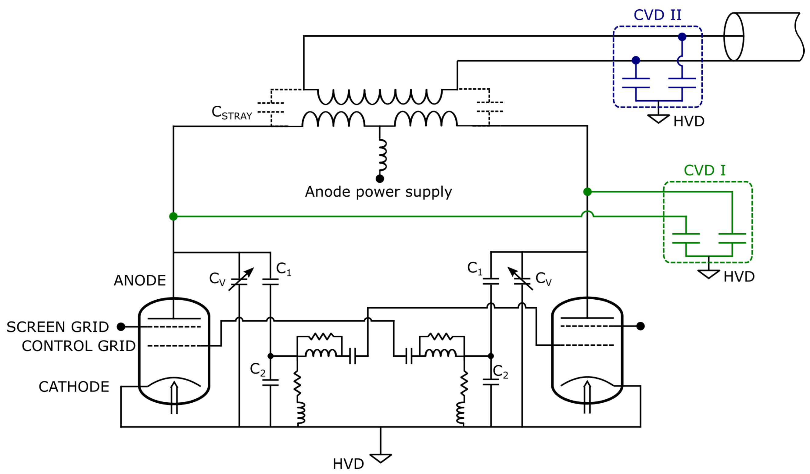
ISRF: Only one ISRF unit is considered in these simulations. The oscillator consists of two Thales IQK 35-2 tetrodes, in the push–pull configuration (
Figure 2). The tetrodes are implemented using an analytical model [
12]; the output power is defined by setting anode voltage (ISRF-TE power supply) and screen grid voltage. In
Figure 2, both CVD configurations are represented (voltage divider at secondary and primary side). Since the divider voltage ratio is large, the CVD is modelled only considering its equivalent capacitance, e.g., the smallest capacitance of the divider. Perfect isolation is assumed between the two legs of the CVD. To move the CVD at the primary side of the transformer, its capacitance (e.g., its gain) was modified in order to obtain a voltage measurement comparable with the one performed at secondary side [
5]; therefore, it could be fed directly into the control loop with small adjustments. The capacitance for a single leg of the CVDs is:
- –
CVD II: C = 250 pF
- –
CVD I: C = 100 pF
Since the CVD installed at the primary becomes part of the oscillator resonant circuit, it is represented just by including it in the variable capacitors ().
The stray capacitance between primary and secondary windings (
) is also represented in the model. The total interwinding capacitance was measured to be 90 pF. In the model, it is represented with two 45 pF capacitors (
in
Figure 2).
A section of RF coaxial line, modeled with the pi-equivalent representation, connects the output of ISRF to the beginning of the TL.
ISBI: only the output filter capacitors of the power supply are modeled. The cables connecting ISBI to the busbars installed in the transmission line are modeled as lumped inductors. A resistor is installed between PGFB and BI busbars before the beginning of the TL.
ISPG: only the output filter capacitors of the power supply are modeled. The busbars from ISPG to the beginning of the transmission line are represented as mutually coupled conductors, with inductive and capacitive parameters per unit length computed by means of the finite element method in FEMM. The coupling with other conductors is not considered inside the HVD.
ISEG: at the output of ISEG, a low-pass R-C filter is installed, to reduce the voltage ripple of the power supply. The inductive component of the filter resistor is considered in the model. ISEG positive pole is locally referred to the HVD by means of a R-C filter. The connection to the transmission line conductors is performed with a shielded medium-voltage cable, which is represented as mutually coupled conductors, with inductive and capacitive parameters per unit length computed by means of the finite element method in FEMM. The inner conductor of the medium-voltage cable is connected to PGFE at the beginning of the transmission line, while the outer shield is connected to HVD potential and to the EG cable of the transmission line.
3.2. Transmission Line
SPIDER TL is represented as a multiconductor transmission line, by means of per unit length equivalent R-L-C blocks, with inductive and capacitive mutual couplings. To correctly simulate the behavior of the TL at the frequency of interest (1 MHz) with the equivalent R-L-C lumped representation, more than 50 elements per wavelength were used in the model [
13]. The reference conductor is chosen to be the outer conductor, described in
Section 2.3. Considering the geometry represented in
Figure 3, the parameters per unit length were computed with FEMM. Details are described in the following section.
Capacitances: the 2D planar electrostatic problem of the TL geometry was analyzed, iteratively applying a unitary voltage to one conductor and fixing the others to zero potential, thus obtaining the Maxwell capacitances matrix. This matrix was then used to obtain the mutual capacitances between conductors.
Inductances: the approach of partial inductances was used to compute the self and mutual inductances of the TL conductors. In FEMM, a Dirichlet boundary condition was imposed at the outer conductor of the TL; thus, we consider that all the currents flowing in the system are contained within that boundary.
Resistances: the RF resistances were computed in FEMM solving the 2D planar magnetic problem, at a frequency of 1 MHz. The current was applied singularly to the conductors.
The distributed core snubber elements were modeled with a multiwinding transformer.
3.3. Beam Source
The source elements represented in the model are the RF load and its interface to the system of grids and other beam-source structures. The load of ISRF, consisting of two RF plasma drivers, is represented by a R-L series. The equivalent resistances and inductances of the RF drivers are not constant and depend upon plasma conditions. The parallel capacitor and two series capacitors represent the matching network. The external conductor of the RF coaxial line is referred to the plasma source body, thus to the BI conductor. The bank of capacitors installed between the PG and the source body, used for mitigation of breakdown overvoltage, is also represented in the model. The system of grids and the electrostatic screen surrounding the source are modeled in terms of their parasitic capacitances.
4. Interpretation of Rf Stray Currents in Spider
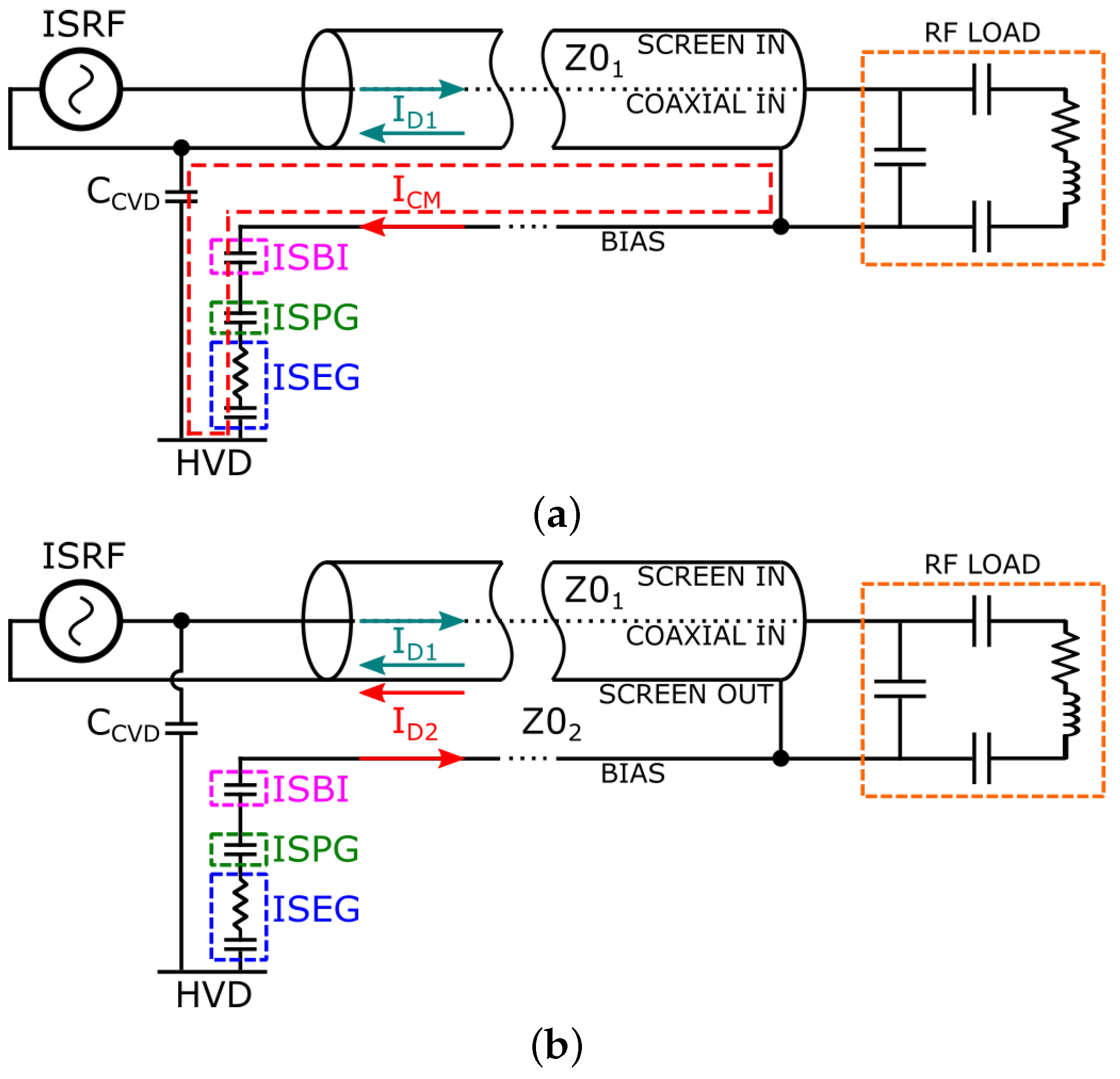
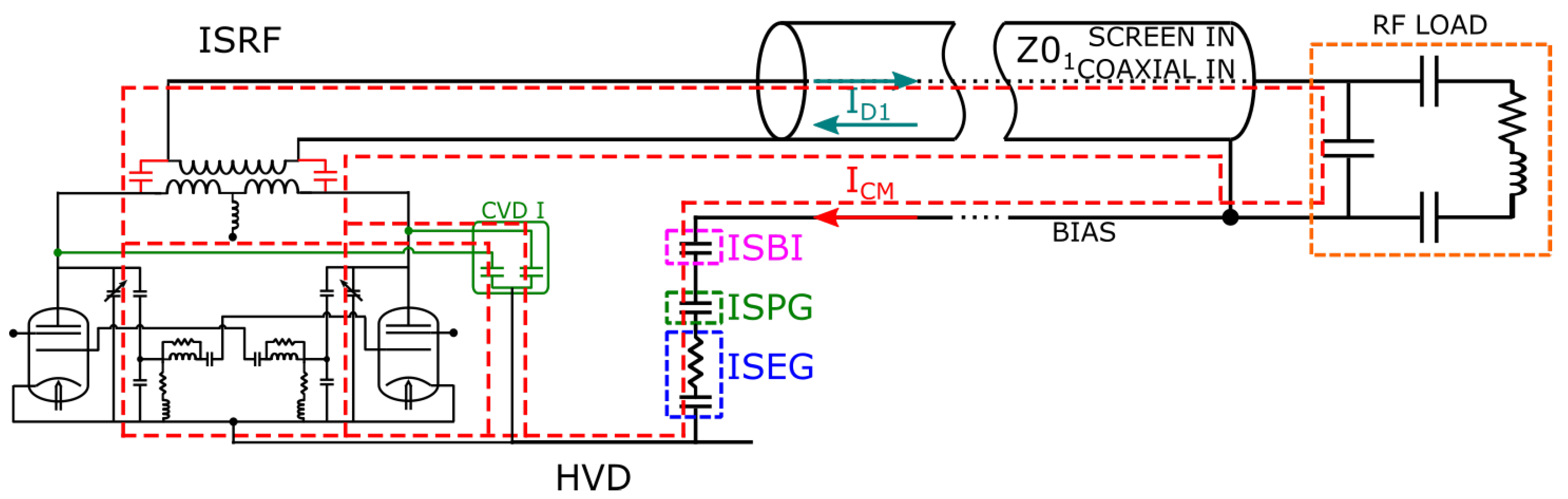
The RF stray currents in SPIDER were originally interpreted as common mode currents, due to the reference to a common potential of both RF source and RF load. Looking more closely at the electric system topology, we can observe that both common mode and differential mode currents can circulate in components external to the RF system, depending on the CVD configuration. We can make a first distinction based on the position of the CVD at the primary or secondary side of the RF transformer.
4.1. CVD at Secondary Side
With the CVD connected at the secondary side, we can further separate the analysis of the RF stray problem in two cases.
CVD outer leg: in SPIDER, the outer conductor of the RF coaxial line has only one physical potential reference, namely the connection to the plasma source. Inside ISRF, the CVD leg connected to the screen of the RF coaxial line (CVD outer leg) provides a high impedance reference to the HVD potential.
Figure 4a represents one of the most direct connections between the reference potentials and the ensuing RF stray current circulation.The common mode current magnitude is defined by the voltage drop across the longitudinal elements of the transmission line and the impedance of the common mode path.
CVD inner leg: the CVD leg connected to the inner conductor of the RF coaxial line (CVD inner leg) allows the circulation of a differential mode current between one of conductors in the transmission line and the outer screen of the RF coaxial line. One of these possible connections is represented in
Figure 4b, where the bias conductor and the outer part of the RF coaxial line screen assume the role of a transmission line with characteristic impedance
, supporting the circulation of a differential current
. In this case, the stray currents magnitude depends on the differential voltage at the secondary side of the RF transformer.
In
Figure 4, the same circuit loop is represented; thus, we can compare these cases to qualitatively understand the relevance of one mode over the other, for the RF stray currents issue. Without considering the resonance phenomenon, we can make the following observations:
Both common mode and differential mode currents are mainly limited by the impedance defined by the CVD leg capacitance. This impedance has the same value for both CVD legs.
The differential mode voltage is significantly larger than the voltage drop across the longitudinal elements of the transmission lines, which defines the common mode voltage.
Thus, when the CVD is connected at the secondary side of the transformer, the main component of RF stray currents is the differential mode current, arising from the connection of the CVD inner leg.
4.2. Cvd at Primary Side
When only CVDI is installed, its capacitance becomes transparent to the oscillator circuit, since it is in parallel with significantly larger capacitors as
and
(see
Figure 2). In addition, when the tetrode is in conduction, one of the branches formed by one CVD leg,
and
is short circuited. In this configuration, a common mode current circulates through the output filters of the power supplies (see a possible path in
Figure 5), due to the stray capacitance between primary and secondary windings of the RF transformer. The common mode current magnitude, in this case, is mainly defined by the impedance of the transformer stray capacitance and the voltage between primary and secondary winding (i.e., the transformer ratio).
5. Rf Stray Currents Simulations
To understand if the representation of SPIDER electrical system presented in
Section 3 is sufficient to describe the problem of RF stray currents in its totality, simulations were carried out with the CVD configuration at primary and secondary side of the ISRF output transformer. Additional simulations were performed in a frequency domain, to evaluate the RF stray currents resonances.
Figure 6 provides an overview of the complete schematics used in simulations.
5.1. Benchmark—Time Domain Simulations
In SPIDER, oscillators cannot work in perfectly matched conditions, due to the frequency flip phenomenon [
14]. The power measurements from ISRF diagnostic and control system are not reliable when the load is unmatched to the generator; thus, a correct estimation of the equivalent RF driver impedance is difficult to obtain. On the other hand, the “unloaded” or “vacuum” impedance of the RF driver, namely the impedance of the RF driver when no plasma is ignited inside the source, is well known. For this reason, only the vacuum pulses are considered to obtain a comparison between experimental results and circuital model. With reference to
Figure 6, the load, matching network and transmission line parameters considered for the vacuum simulation are the following:
H
nF
nF
For the ISRF unit considered, the length of the RF coaxial line from oscillator to load is 43 m. The load, matching network and RF coaxial line parameters are obtained by fitting the impedance measurement performed at the beginning of the RF coaxial line, over the operating frequency range, to the equivalent RF circuit model. The ISRF representation used for the time domain simulations is the one of
Figure 2, with the oscillator modeled in its entirety. The experimentally measured screen grid voltage, anode voltage and tuning capacitance (
) are used as simulation inputs.
Table 1 collects the results obtained from current measurements (RMS values) performed at the ISEG output filter branch (
, see
Figure 6), and from simulations. The simulation is performed in time domain, and the results reported are relative to oscillator steady-state conditions (constant frequency and output power).
The differences between measured and simulated oscillator output voltage and current that we can observe in
Table 1 are mainly due to the imprecise characterization of the output RF transformer; additional dedicated measurements are performed to refine the representation of primary, secondary and mutual inductances of the transformer. Despite the challenges in representing correctly also ISEPS conductors not intended for transmission of RF power and RF stray connections in the beam source, the model provides reasonable results, when comparing to the specific operating condition defined in this section. To test the limitations of the model and to understand if additional components need to be introduced in the simulation to provide a correct depiction of the RF stray currents behavior, it would be necessary to perform measurements in several locations of SPIDER ISEPS (e.g., current measurement for all the conductors of the transmission line) and in the whole operating frequency range. The experimental activities are underway to assess the RF stray currents frequency response in the operating range.
5.2. Frequency Domain Simulations
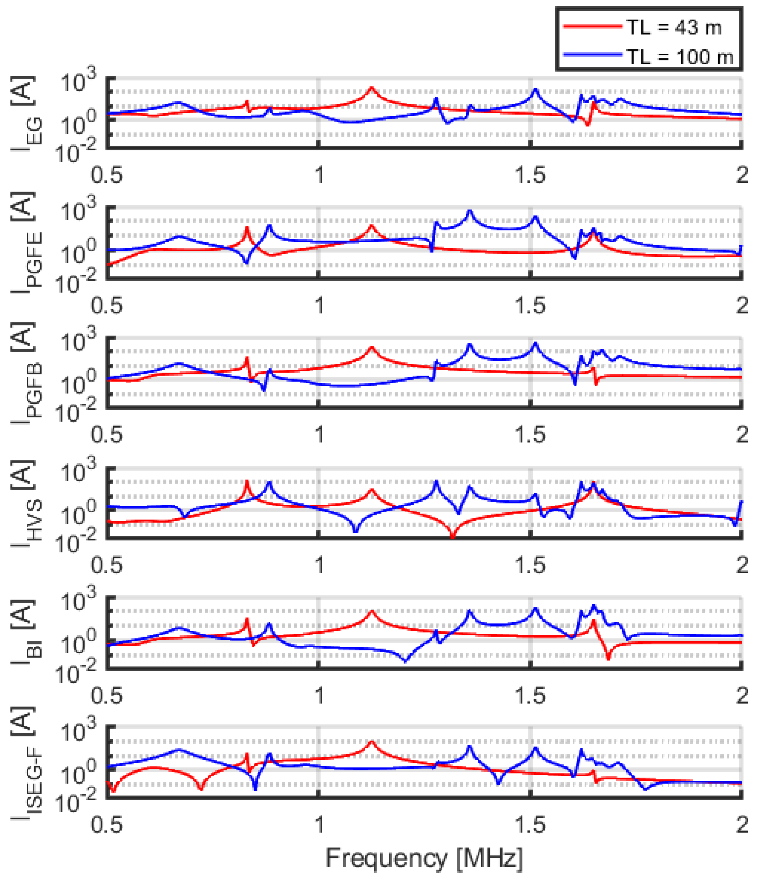
For the frequency domain simulations, a simplified approach was used: we assume that when CVD II is installed, the RF stray currents are mostly confined to the secondary side of the RF transformer, referred to HVD through the capacitive divider. Thus, only the secondary can be represented using an ideal voltage source. Inevitably, these simulations can be carried out only for the case of CVD installed at the secondary. Performing the simulations in an extended frequency range points out the presence of resonance peaks for the RF stray currents.
Figure 7 shows the resonances of the stray currents flowing through all the conductors of the transmission line and through ISEG filter. Two transmission line lengths are considered, one representing the current SPIDER configuration (43 m) and one resembling MITICA transmission line [
15] (100 m).
The relative position of the resonance peaks from the working frequency range determines the entity of unwanted RF currents flowing in the electrical system. If a resonance is brought within the operating frequencies, potentially dangerous working conditions can arise, leading to overloads in electrical equipment not intended to operate with RF power.
Being able to preemptively identify and avoid these resonances in SPIDER also permit applying this analysis process to the case of MITICA, which presents several differences with respect to SPIDER (transmission line length, layout of conductors and components inside the beam source).
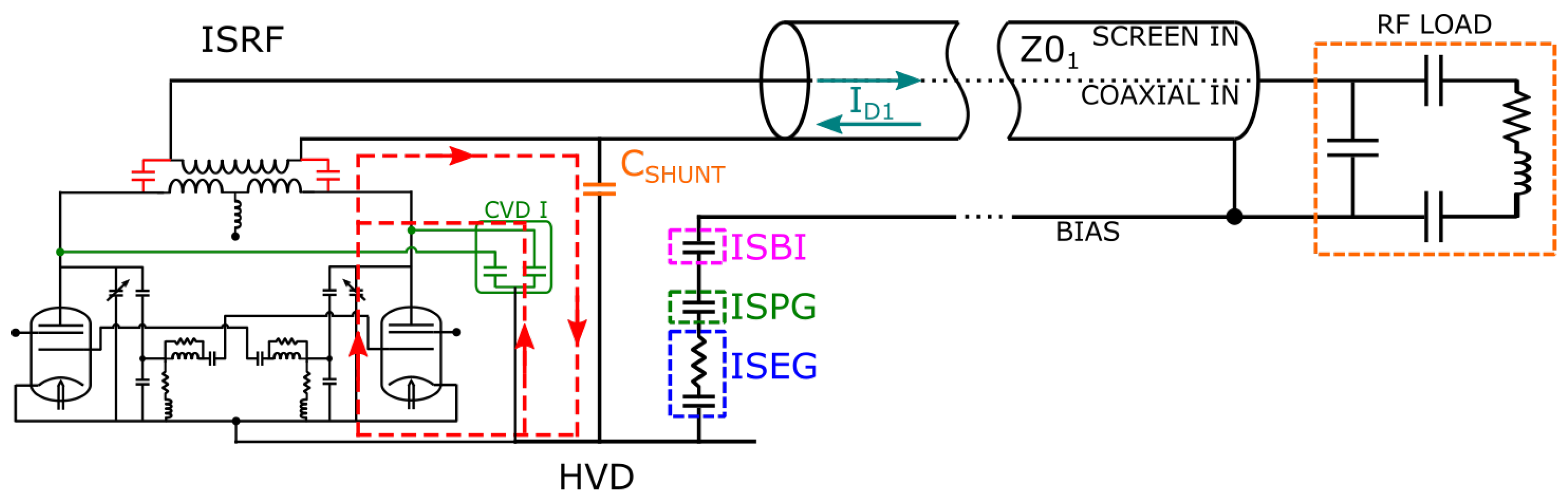
5.3. Minimization of Rf Stray Currents
Based on the observations made in
Section 4.1 and
Section 4.2, simulations were carried out with the model presented in
Section 5.1, comparing the RF stray current through ISEG output filter. All the simulations are carried out with the same ISRF output conditions; only the CVD configuration is changed.
We can see from
Table 2 that the main contribution of RF stray currents when CVDII is installed comes from differential mode currents, due to the connection of one CVD leg to the inner conductor of the RF coaxial line. Since the CVDII outer leg connection does not contribute significantly to the circulation of RF stray currents, we can make a consideration for the further reduction of RF stray currents through ISEPS components, when the CVD is connected at the primary of ISRF transformer: a capacitor can be installed between the outer conductor of the coaxial line and HVD to shunt directly inside ISRF cubicle the common mode current caused by the stray capacitance between primary and secondary of the RF transformer (see
Figure 8).
Figure 9 shows that the shunt capacitor can further reduce the electrical stress caused by the circulation of RF stray currents on ISBI, ISPG and ISEG output filter components.
6. Conclusions
In this paper, we described the development of a circuital model for the study of RF stray currents in SPIDER and MITICA electrical system. Achieving a good comparison with measurements is not simple, due to the difficulty in correctly representing connections, as well as stray parameters, in the whole system. Nonetheless, the simulation platform allows one to investigate the RF stray current behavior and the validity of proposed solutions for its minimization. An alternative interpretation of RF stray currents origin in SPIDER was discussed, with respect to the initial description based on common mode currents, in order to provide a better view on the causes of this phenomenon.
Author Contributions
Conceptualization, R.C., M.D. and A.M.; methodology, A.M., M.D., M.R. and R.C.; software, R.C. and M.D.N.; validation, R.C. and M.D.N.; investigation, M.D. and R.C.; writing—original draft preparation, R.C.; writing—review and editing, A.M., M.D., M.R. and R.C.; visualization, R.C. All authors have read and agreed to the published version of the manuscript.
Funding
The views and opinions expressed herein do not necessarily reflect those of the ITER Organization. This work was carried out within the framework of the EUROfusion consortium and received funding from the Euratom research and training programme 2014–2018 and 2019–2020 under grant agreement No. 633053. The views and opinions expressed herein do not necessarily reflect those of the European Commission.
Institutional Review Board Statement
Not applicable.
Informed Consent Statement
Not applicable.
Data Availability Statement
The data presented in this study are available on request from the corresponding author.
Conflicts of Interest
The authors declare no conflict of interest.
References
- Toigo, V.; Piovan, R.; Dal Bello, S.; Gaio, E.; Luchetta, A.; Pasqualotto, R.; Zaccaria, P.; Bigi, M.; Chitarin, G.; Marcuzzi, D.; et al. The PRIMA test facility: SPIDER and MITICA test-beds for ITER neutral beam injectors. New J. Phys. 2017, 19, 085004. [Google Scholar] [CrossRef] [Green Version]
- Toigo, V.; Marcuzzi, D.; Serianni, G.; Boldrin, M.; Chitarin, G.; Dal Bello, S.; Grando, L.; Luchetta, A.; Pasqualotto, R.; Zaccaria, P.; et al. On the road to ITER NBIs: SPIDER improvement after first operation and MITICA construction progress. Fusion Eng. Des. 2021, 168, 112622. [Google Scholar] [CrossRef]
- Serianni, G.; Toigo, V.; Bigi, M.; Boldrin, M.; Chitarin, G.; Dal Bello, S.; Grando, L.; Luchetta, A.; Marcuzzi, D.; Pasqualotto, R.; et al. First operation in SPIDER and the path to complete MITICA. Rev. Sci. Instrum. 2020, 91, 023510. [Google Scholar] [CrossRef] [PubMed]
- Maistrello, A.; Recchia, M.; Zamengo, A.; Bernardi, M.; Chitarin, G.; Dan, M.; Gasparini, F.; Jain, P.; Bigi, M.; Gaio, E.; et al. Improvements in the SPIDER RF system. Fusion Eng. Des. 2021, 167, 112337. [Google Scholar] [CrossRef]
- Maistrello, A. On the Effectiveness of SPIDER RF System Improvements. In Proceedings of the 29th IEEE Symposium on Fusion Engineering (SOFE 2021), Denver, CO, USA, 12–16 December 2021. [Google Scholar]
- Zanotto, L. Radio Frequency Generators Based on Solid State Amplifiers for the NBTF and ITER Projects. In Proceedings of the 29th IEEE Symposium on Fusion Engineering (SOFE 2021), Denver, CO, USA, 12–16 December 2021. [Google Scholar]
- Boldrin, M.; Toigo, V.; Gutierrez, D.; Simon, M.; Faoro, G.; Maggiora, E.; Pedron, D.; Guion, A.; Decamps, H. The Transmission Line for the SPIDER Experiment: From design to installation. Fusion Eng. Des. 2017, 123, 247–252. [Google Scholar] [CrossRef]
- Bigi, M.; Rinaldi, L.; Simon, M.; Sita, L.; Taddia, G.; Carrozza, S.; Decamps, H.; Luchetta, A.; Meddour, A.; Moressa, M.; et al. Design, manufacture and factory testing of the Ion Source and Extraction Power Supplies for the SPIDER experiment. Fusion Eng. Des. 2015, 96, 405–410. [Google Scholar] [CrossRef]
- Bigi, M.; De Lorenzi, A.; Grando, L.; Watanabe, K.; Yamamoto, M. A model for electrical fast transient analyses of the ITER NBI power supplies and the MAMuG accelerator. Fusion Eng. Des. 2009, 84, 446–450. [Google Scholar] [CrossRef]
- Pesce, A.; De Lorenzi, A.; Boldrin, M. Passive protections against breakdowns between accelerating grids in SPIDER experiment. Fusion Eng. Des. 2011, 86, 847–850. [Google Scholar] [CrossRef]
- Zamengo, A.; Pesce, A.; Bigi, M. Overvoltage protection of the Ion source and extraction power supplies in the SPIDER experiment. In Proceedings of the 2011 IEEE/NPSS 24th Symposium on Fusion Engineering, Chicago, IL, USA, 26–30 June 2011; pp. 1–6. [Google Scholar]
- Zheng, S.; Keane, J. Modeling and Simulation of the Power Amplifier for the RHIC 28 MHz Accelerating Cavity; Technical Report; Brookhaven National Laboratory (BNL) Relativistic Heavy Ion Collider, USA. 2003. Available online: https://www.osti.gov/biblio/1061690/ (accessed on 19 November 2021). [CrossRef] [Green Version]
- Cui, W.; Shi, H.; Luo, X.; Sha, F.; Drewniak, J.; Van Doren, T.; Anderson, T. Lumped-element sections for modeling coupling between high-speed digital and I/O lines. In Proceedings of the IEEE 1997 International Symposium on Electromagnetic Compatibility, Symposium Record (Cat. No.97CH36113), Austin, TX, USA, 18–22 August 1997; pp. 260–265. [Google Scholar] [CrossRef]
- Gasparini, F.; Recchia, M.; Bigi, M.; Patton, T.; Zamengo, A.; Gaio, E. Investigation on stable operational regions for SPIDER RF oscillators. Fusion Eng. Des. 2019, 146, 2172–2175. [Google Scholar] [CrossRef]
- Tobari, H.; Kashiwagi, M.; Watanabe, K.; Maejima, T.; Yamashita, Y.; Dairaku, M.; Oda, Y.; Sasaki, S.; Kojima, A.; Umeda, N.; et al. Completion of DC 1 MV power supply system for ITER neutral beam test facility. In Proceedings of the 27th IAEA Fusion Energy Conference, Ahmedabad, India, 22–27 October 2018. [Google Scholar]
Figure 1.
Representation of the overall electrical system of SPIDER. From left to right: AGPS, HVD and ISEPS—transmission line—beam source.
Figure 1.
Representation of the overall electrical system of SPIDER. From left to right: AGPS, HVD and ISEPS—transmission line—beam source.
Figure 2.
Detail of ISRF unit. The original CVD configuration (CVD II) and the modified one (CVD I) are both represented.
Figure 2.
Detail of ISRF unit. The original CVD configuration (CVD II) and the modified one (CVD I) are both represented.
Figure 3.
SPIDER transmission line considered in the circuital model. (a) SPIDER TL cross-section (not in scale). (b) Equivalent pi-representation of the multiconductor TL.
Figure 3.
SPIDER transmission line considered in the circuital model. (a) SPIDER TL cross-section (not in scale). (b) Equivalent pi-representation of the multiconductor TL.
Figure 4.
RF stray current paths with CVD installed at RF transformer primary side. (a) Common mode current related to the connection of one CVD leg to the outer conductor of the RF coaxial line. (b) Differential mode current related to the connection of one CVD leg to the inner conductor of the RF coaxial line.
Figure 5.
Common mode current path with CVD installed at RF transformer primary side.
Figure 5.
Common mode current path with CVD installed at RF transformer primary side.
Figure 6.
Complete scheme of the circuital model. In red, the stray elements, and in blue, the position of the voltage and current measurements ().
Figure 6.
Complete scheme of the circuital model. In red, the stray elements, and in blue, the position of the voltage and current measurements ().
Figure 7.
RF stray current resonances in SPIDER transmission line conductors and ISEG filter, in configuration with CVD installed at the secondary side of ISRF transformer. Two transmission line lengths are considered in the simulation, 43 and 100 m.
Figure 7.
RF stray current resonances in SPIDER transmission line conductors and ISEG filter, in configuration with CVD installed at the secondary side of ISRF transformer. Two transmission line lengths are considered in the simulation, 43 and 100 m.
Figure 8.
Shunting of the common mode current through a capacitor installed between RF coaxial line outer conductor and ISRF cubicle (HVD).
Figure 8.
Shunting of the common mode current through a capacitor installed between RF coaxial line outer conductor and ISRF cubicle (HVD).
Figure 9.
Reduction of RF stray current (RMS value) through ISEG output filter due to the installation of a shunt capacitor between RF coaxial outer conductor and ISRF cubicle.
Figure 9.
Reduction of RF stray current (RMS value) through ISEG output filter due to the installation of a shunt capacitor between RF coaxial outer conductor and ISRF cubicle.
Table 1.
Comparison between measurements performed in SPIDER (EXP) and circuital simulation (SIM) in the original (CVD II) and modified (CVD I) configurations. The figure of merit for the RF stray currents is the current measured at the ISEG output filter branch (). All the voltage and current values are RMS.
| | | [V] | [A] | f [MHz] | [A] |
|---|
| CVDII | EXP | 2500 | 25 | 0.933 | 2.92 |
| SIM | 2490 | 31 | 0.94 | 3.07 |
| CVDI | EXP | 2250 | 27 | 0.935 | 1.16 |
| SIM | 2200 | 29.3 | 0.94 | 1.5 |
Table 2.
Simulation of current through ISEG filter in different CVDII configurations: the connections of only inner and outer leg of the CVD are tested against the full CVD.
Table 2.
Simulation of current through ISEG filter in different CVDII configurations: the connections of only inner and outer leg of the CVD are tested against the full CVD.
| CVD II | FULL | INNER LEG | OUTER LEG |
|---|
| I | I | 1.06 I | 0.15 I |
| Publisher’s Note: MDPI stays neutral with regard to jurisdictional claims in published maps and institutional affiliations. |
© 2021 by the authors. Licensee MDPI, Basel, Switzerland. This article is an open access article distributed under the terms and conditions of the Creative Commons Attribution (CC BY) license (https://creativecommons.org/licenses/by/4.0/).


 ,
, 


