Article

Single-Mode Polymer Ridge Waveguide Integration of Organic Thin-Film Laser

1
Institut für Hochfrequenztechnik, Technische Universität Braunschweig, Schleinitzstraße 22, 38106 Braunschweig, Germany
2
Freiburger Zentrum für interaktive Werkstoffe und bioinspirierte Technologien, Universität Freiburg, Georges-Köhler-Allee 105, 79110 Freiburg, Germany
*
Author to whom correspondence should be addressed.
Current address: Cluster of Excellence PhoenixD (Photonics, Optics, and Engineering – Innovation Across Disciplines), 30167 Hannover, Germany.
Appl. Sci. 2020, 10(8), 2805; https://doi.org/10.3390/app10082805
Submission received: 6 March 2020 / Revised: 14 April 2020 / Accepted: 16 April 2020 / Published: 18 April 2020

Abstract

:
Organic thin-film lasers (OLAS) are promising optical sources when it comes to flexibility and small-scale manufacturing. These properties are required especially for integrating organic thin-film lasers into single-mode waveguides. Optical sensors based on single-mode ridge waveguide systems, especially for Lab-on-a-chip (LoC) applications, usually need external laser sources, free-space optics, and coupling structures, which suffer from coupling losses and mechanical stabilization problems. In this paper, we report on the first successful integration of organic thin-film lasers directly into polymeric single-mode ridge waveguides forming a monolithic laser device for LoC applications. The integrated waveguide laser is achieved by three production steps: nanoimprint of Bragg gratings onto the waveguide cladding material EpoClad, UV-Lithography of the waveguide core material EpoCore, and thermal evaporation of the OLAS material Alq3:DCM2 on top of the single-mode waveguides and the Bragg grating area. Here, the laser light is analyzed out of the waveguide facet with optical spectroscopy presenting single-mode characteristics even with high pump energy densities. This kind of integrated waveguide laser is very suitable for photonic LoC applications based on intensity and interferometric sensors where single-mode operation is required.

Graphical Abstract

1. Introduction

The light from only a few light sources is able to couple effectively into single-mode waveguides. Lasers are light sources with very high coupling efficiencies. For polymeric waveguides, however, not all laser types are suitable. Especially for LoC devices, single-mode operation is mostly required. The coupling of the laser light into the single-mode waveguide is mainly achieved by prism-coupling, grating couplers with a free-space set-up or butt-coupling with a lensed fiber [1]. An important step towards waveguide integrated lasers can be realized by combining the laser resonator, such as distributed feedback resonator (DFB) with the waveguide structure. The DFB wavelength selectivity and high efficiency as well as the ease of fabrication makes them very suitable for this kind of integration. OLAS are well suited for this application due to their low layer thickness, their flexibility and simple processing [2]. In the last decade, the integration of organic DFB lasers into waveguides and LoC systems has been demonstrated. Balslev et al. [3] realized a LoC system with an integrated organic laser source and a photodiode. The laser light source is achieved by the laser dye Rhodamine 6G dissolved in ethanol, which is purged through a microfluidic channel to a DFB grating. The integration of the laser source and the multi-mode SU-8 waveguides is realized by butt coupling. Christiansen et al. [4] reported on active and passive SU-8 waveguides either doped or undoped with the laser dye Rhodamine 6G. First, the active waveguide is constructed by a lithography and imprint process. The following passive waveguide is subsequently built up and also butt coupled to the active waveguide. Mappes et al. [5] and Vannahme et al. [6] report on an integration of an OLAS into PMMA. The resonant DFB structure is formed by the aid of hot-embossing and the waveguides are manufactured by deep UV irradiation of the PMMA bulk material. Up to now, all the integrations are only realized with multi-mode waveguides or slab waveguides. However, it is a great approach for intensity based LoC applications where, for example, fluorescence excitation of an analyte in a microfluidic channel is used. Despite that, pure single-mode operations is required for interferometric based sensors such as optical based LoC-systems. Since higher modes propagate with different speed of light and have different evanescent wave characteristics, this leads to an inefficient interferometric interaction in the sensor as well as signal losses due to modal dispersion [1]. Recently Becker et al. [7] integrated DFB gratings onto a 2.0 m in width and 2.5 m in height few-mode ridge waveguide. This is realized by a straightforward combined nanoimprint and photolithography process (CNP process) using OrmoCore, a silicon-containing hybrid waveguide core material. On it, the OLAS is finally evaporated. In our study, we used a three-step fabrication process to integrate the OLAS into the 1.0 m in width and 1.0 m in height polymeric single-mode waveguide as schematically depicted in Figure 1a. Therefore, we used the photopatternable epoxies EpoClad (refractive index = 1.579 @650 nm) and EpoCore (refractive index = 1.593 @650 nm) for the cladding layer including the grating structure and the waveguide core, respectively. The waveguide materials are commercially available and distributed by Micro Resist Technology GmbH in Germany. The active organic material (Alq3:DCM2) was then evaporated on top of the waveguide structure with the DFB gratings underneath. The final device contains five DFB gratings in parallel and five single-mode waveguides on top of each grating area, forming 25 different waveguide integrated lasers with five different emission wavelengths.

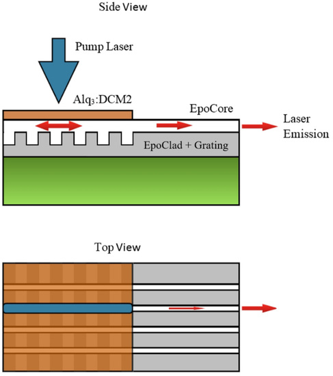
2. The Polymeric Single-Mode Waveguide

Optical simulations using the finite difference eigenmode solver support the single-mode characteristic. Figure 2 shows the cross section of the single-mode ridge waveguide structure as described in the introduction as well as the TE0 and TE1 mode distribution with air (refractive index ≈1.0002 @650 nm) and EpoClad as the surrounding cladding medium.
For the ridge-type waveguide with air as upper cladding, the TE0 mode is asymmetric and extends into the lower cladding (see Figure 2a). The effective refractive index was calculated to be 1.561 @650 nm. Figure 2b shows the TE0 mode distribution for the symmetrical case where the waveguide core is surrounded by the cladding material making it a buried waveguide. The mode field maximum is located in the waveguide core and the minority of the field intensity is located to be outside and is called evanescent field. In this structure, the decay length of the evanescent field is about 1 m. For the buried waveguide, the effective refractive index of the TE0 mode is 1.58 @650 nm. In both cases, higher modes such as TE1 (see Figure 2c,d) are not capable of propagation in the waveguide core.

3. The Organic Thin-Film Laser

We used the well-known guest–host active organic laser material containing Tris-(8-hydroxyquinoline)aluminum (Alq3) as the host material and the laser dye 4-(Dicyanomethylene)-2-methyl-6-julolidyl-9-enyl-4H-pyran (DCM2) as the guest material (see Figure 1b). Figure 3 shows the photoluminescence spectra (PL spectra) of Alq3 and Alq3:DCM2 with different DCM2 doping concentrations. The samples were evaporated and characterized on glass substrates.
Figure 3 shows a redshift in the emission spectra of the Alq3:DCM2 samples with increasing DCM2 doping concentration. The reason for this is the Solid State Solvation Effect (SSSE). It describes the polarity influence of the host matrix on the emitter molecule [8]. Furthermore, Figure 3 also shows a decreased Alq3 emission in the PL spectra with increasing doping concentration of DCM2. The fraction of Alq3 emission is about 18% (see dashed line in Figure 3) with the DCM2 doping concentration of 1%. When the doping concentration increases to 3%, the fraction of Alq3 emission drops to 5%. With further increasing of the doping concentration, as shown in Figure 3, the Alq3 emission fraction in the PL spectra drops even more. This is due to the Förster resonant energy transfer [9,10] where with decreasing donor/acceptor mean distance the probability of a resonant energy transfer increases. The great advantages of this material system are the broad optical laser tuning range of up to 115 nm, low lasing threshold down to approximately 3 µJ/cm 2 , and high optical gain, which saturates at about 300 cm 1 [11,12,13]. Moreover, the Alq3:DCM2 thin-film is characterized by its absolutely smooth surface after the vapor deposition process. The surface roughness was measured to be Ra = 950 pm (arithmetic mean value) and Rq= 1.2 nm (root mean square value). However, surface roughness, morphological variations as well as the pump process itself can cause slightly stochastic fluctuations and noise in the signal. Therefore, in the spectral analysis, the Karhunen–Loève Transformation can be applied [14]. Different kinds of resonating structures could be demonstrated to achieve lasing in organic thin-films, such as DFB resonators, micro disks, spheres, and distributed Bragg reflectors (DBR) [15,16,17,18,19]. The DFB resonator, however, stands out because of its ease of fabrication and its optical properties such as the extraordinary wavelength selectivity and high efficiency. The emission wavelength ( λ Bragg ) of the distributed feedback laser can be varied by choosing the suitable grating periodicity Λ . It follows the Bragg condition:
λ Bragg = 2 · n eff · Λ m ,
where neff is the effective refractive index of the allover waveguide structure, Λ is the grating period, and m = 1 , 2 , 3 , . . . , is the diffraction order.

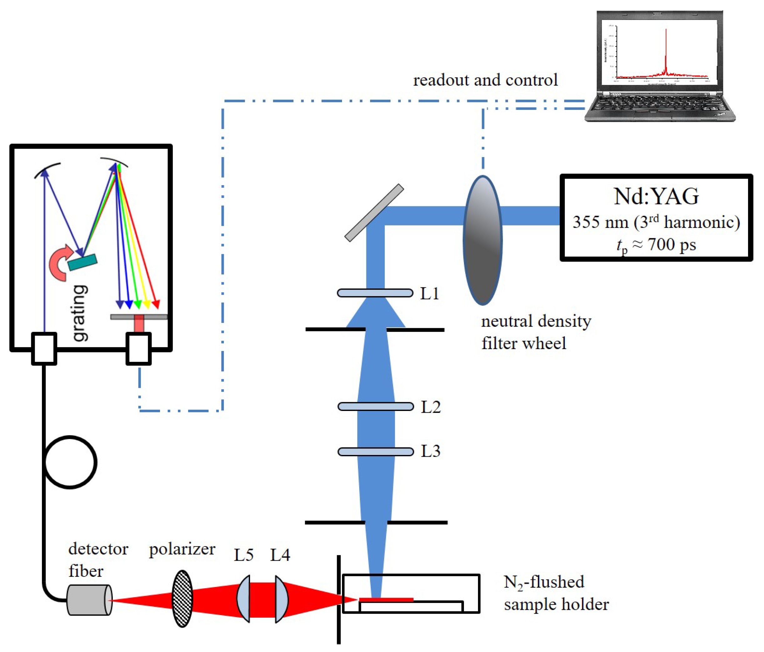
4. Device Fabrication

First, a Polydimethylsiloxan (PDMS) stamp was made for replication of the DFB gratings. The grating area contains five DFB gratings arranged in parallel, with the dimension of 2 mm in width and 10 mm in length. The periodicity of the gratings was 195 nm to 215 nm with a period spacing of 5 nm. After the fabrication of the PDMS stamp, the bottom cladding with the grating structures was fabricated by a UV nanoimprint process. In this step, a mixture of EpoClad and γ -Butyrolactone (GBL) with a mixing ratio of 2:1 was used. The GBL diluted EpoClad was spin-coated onto a silicon wafer with 4000 rpm for 30 s and then soft baked at 120 C for 2 min on a hot plate. After the soft bake, the PDMS stamp was brought into contact with the still sticky EpoClad. A subsequent flood-exposure starts the UV-induced cross-linking of the polymer. After that, the substrate was baked again on a hot plate at 120 C for 3 min. After the EpoClad was completely polymerized, the silicon-PDMS stamp set was taken from the hot plate and the PDMS stamp was removed without any residue. The layer thickness of EpoClad was about 1 m. Figure 4a shows the profile of one of the gratings with Λ = 195 nm and Figure 4b shows a good replication quality. This image was taken with an atomic force microscope. The measured average periodicity is 194.97 nm, which is extremely close to the desired value.
The next fabrication step is structuring the waveguides onto the DFB gratings. In this case, a mixture of EpoCore and γ -Butyrolactone (GBL) in a mixing ratio of 2:1 was used. The mixture was spin-coated with 4600 rpm for 30 s onto the substrates with the pre-structured cladding layer. The substrates were first baked at 50 C and then at 90 C for 2 min each followed by a UV-lithography step using a chromium mask with the waveguide structures. After that, the substrates were put on the hot plate again for 2 min at 50 C and for 3 min at 85 C for a post-exposure bake. The non-cross-linked EpoCore was removed by dipping it for 10 s into the mr-Dev 600 developer. Finally, the substrates were rinsed in isopropyl alcohol to stop the development process. Figure 5 shows schematic sketch of the final device.
Before starting the measurements, the final device was carved at the break points with a diamond scriber so that the silicon wafer split apart along its crystal lattice. Figure 6 presents the SEM images of the EpoCore waveguide on top of the DFB gratings.
The figures show a good waveguide integration on top of the DFB gratings as well as a satisfying waveguide end facet for the optical analysis of the integrated waveguide laser. Figure 6a also gives a detailed look at the waveguide and shows some irregularities and an uneven surface. This can probably be addressed to the grating structure below. The waveguides outside this grating area show good optical quality and a smooth surface (cf. Figure 6b). After the fabrication of the DFB gratings and the waveguides, 200 nm of the guest–host laser active material system Alq3:DCM2 with a DCM2 doping concentration of 6% was co-evaporated in an ultrahigh vacuum chamber with p < 10 8 mbar by organic molecular beam deposition method.

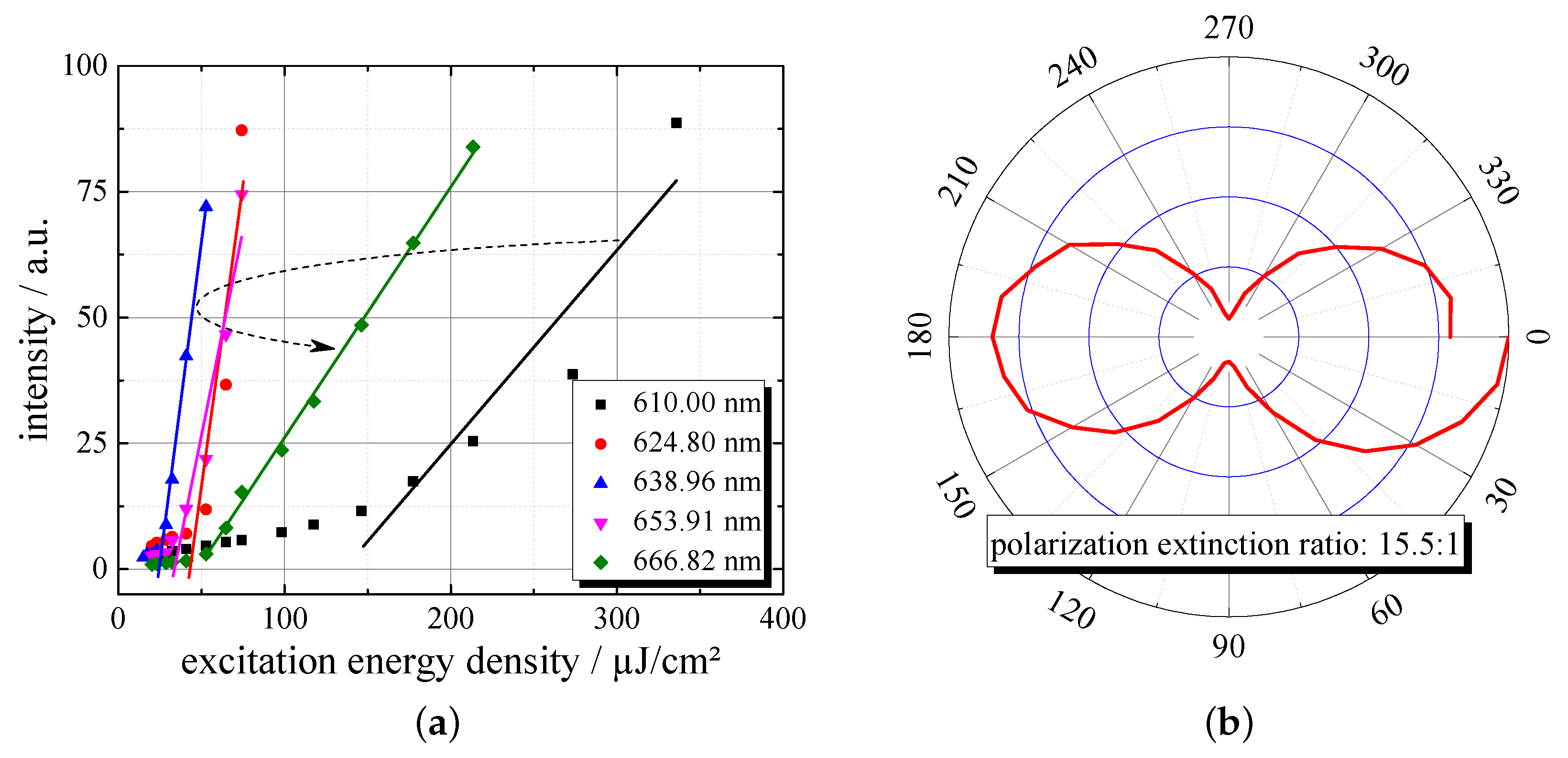
5. Results and Discussion

The samples were measured and characterized by the optical set-up schematically shown in Figure 7.
The waveguide integrated OLAS was excited with the third harmonic ( λ 3 = 355 nm) of a passively Q-switched Nd:YAG laser. The excitation energy was controlled by a neutral density filter. For an efficient excitation, the Gaussian beam out of the Nd:YAG laser was formed into a laser stripe by the cylindrical lenses L1, L2, and L3. Additional apertures form a flat-top profile out of the Gaussian beam. Thus, an excitation stripe of 0.15 mm in width and 3.0 mm in length was created. The dimensions of the laser stripe were measured with a Thorlabs BP209-VIS/M scanning-slit optical beam profiler. The energy out of the pump laser was measured with the Coherent LabMax-Top system. The waveguide integrated laser probes were stored and measured in a N2-flushed chamber. Instead of this method, to avoid unnecessary degradation and oxidation under atmosphere conditions, a thin-film encapsulation can be applied on top of the waveguide integrated lasers [20]. The excited laser emission out of the end facet of the waveguide was measured by using the lens pair L4 and L5. An additional aperture at the N2-flushed chamber in front of the Lens L4 was included to suppress the scattered light. The waveguide integrated lasers were analyzed by a precise monochromator (Triax 320, HORIBA Scientific) and a liquid nitrogen cooled CCD detection system (Symphony, HORIBA Scientific).
The measurement of the OLAS out of the waveguide facet is depicted in Figure 8a, where lasing occurred with all grating periods. For the sake of simplicity, we took a closer look at just one laser line. Figure 8b shows the laser line at λ Bragg = 640.24 nm . Using the Bragg condition in Equation (1) for the first order laser emission ( m = 1 ) at Λ = 205 nm, an effective refractive index n eff of about 1.562 can be determined. This result is comparable with the result of the mode propagation simulation. The effective refractive index n eff of the fundamental mode for this waveguide was calculated to be approximately 1.561 @640 nm. The spectral width of the emission peak at the full width at half maximum (FWHM) was measured to be 200 pm. Furthermore, by increasing the excitation energy density up to 274 J/cm2 (cf. Figure 8c), no further modes except the fundamental mode were found. In previous measurements on few-mode waveguides (waveguide facet dimension 2 × 2 m 2 ), up to five modes could be found with increased pump energy.
Deviating from the DFB theory [21,22], where two laser modes near the Bragg wavelength are generated due to the symmetry of the gratings in index-coupled DFB-lasers [23], we could only measure one laser line out of our waveguide integrated lasers. We suppose that this effect can be addressed to the replication process of the Bragg grating structure into the polymeric cladding layer. Possible slight thickness variations of the polymer layers due to the spin-coating technique as well as potential variations in the doping concentration of the active laser material can have an effect on the effective refractive index change in the structure leading to an asymmetrical behavior and therefore to single-mode operation of the waveguide integrated laser.
Figure 9a shows the emitted intensity of the waveguide integrated lasers in dependence of the excitation energy density. An increased laser emission could be found by exceeding the lasers above their laser thresholds. Laser thresholds could be found to be in the range from approximately 25 J/cm2 to approximately 170 J/cm2. Moreover, with increasing the Bragg grating period, and therefore increasing the laser wavelength, the laser threshold decreases and the slope of the lasers increases. At a certain turning point, the laser threshold increases and the laser slope decreases. This can be attributed to the spectral response of the optical modal gain of this material (cf. Figure 8a). The turning point corresponds with the modal gain maximum where the stimulated cross section is the highest [12,13]. The spectral width of the modal gain increases with increasing excitation energy density. Thus, for shorter laser wavelengths, higher excitation energy is needed until the optical modal gain overcomes absorption and optical losses. For higher wavelengths, the optical modal gain decreases, which can be seen in the laser threshold of the laser with 666.82 nm laser wavelength. The lowest lasing threshold is one magnitude higher than classic OLAS without waveguides (cf. [2]) but still up to 210-times lower than the thresholds reported in [3,4]. By inserting a polarization filter in front of the detection fiber into the optical set-up (cf. Figure 7), a polarization measurement could be done to get the TE- and TM-proportions. The radiated emission was clearly linear polarized with a polarization extinction ratio (PER) of 15.5 : 1 . The intensity difference between the values at 0 and 360 can be addressed to a slight degradation of the sample during this measurement.

6. Conclusions

In this study, EpoCore and -Clad based single-mode waveguides with integrated Bragg gratings were successfully fabricated. By depositing the organic laser material Alq3:DCM2 on top of the waveguide structure, a monolithically single-mode waveguide laser device is achieved. The laser emission could be measured at all waveguide integrated lasers with a FWHM of 200 pm. No other higher modes could be observed even with excitation energy densities up to 274 J/cm2. The laser threshold could be measured to be in a range of approximately 25 J/cm2 to 170 J/cm2. The LoC application ability for photonic or interferometric based sensors could be supported by the polarization extinction ratio of 15.5:1, which indicts a linear polarization. By using this type of laser with the described integration, light can be easily coupled into the single-mode waveguide. This type of laser integration allows an uncomplicated light coupling into a single-mode waveguide. With this work, a milestone towards the monolithically integration of organic lasers is achieved. Especially, optical sensor systems based on single-mode waveguides and, in particular, LoC systems could benefit from this work.

Author Contributions

Conceptualization: M.Č.; software: M.Č.; validation: M.Č., J.B. and O.C.; investigation: M.Č. and J.B.; writing—original draft preparation: M.Č.; writing—review and editing: J.B. and H.-H.J.; supervision: H.-H.J., C.M. and W.K.; All authors have read and agreed to the published version of the manuscript.

Funding

The authors would like to thank the German Research Foundation (Deutsche Forschungsgemeinschaft, DFG) for funding this work within the PolySens Project (Project ID 410203759) as well as the Germany’s Excellence Strategy within the Cluster of Excellence PhoenixD (EXC 2122, Project ID 390833453).

Acknowledgments

The authors would like to acknowledge the contribution of the SEM measurements used in this publication by M.Sc. Jan Gülink from the Institut für Halbleitertechnik, TU Braunschweig.

Conflicts of Interest

The authors declare no conflict of interest.

References

  1. Estevez, M.; Alvarez, M.; Lechuga, L. Integrated optical devices for lab-on-a-chip biosensing applications. Laser Photonics Rev. 2012, 6, 463–487. [Google Scholar] [CrossRef] [Green Version]
  2. Kuehne, A.J.C.; Gather, M.C. Organic Lasers: Recent Developments on Materials, Device Geometries, and Fabrication Techniques. Chem. Rev. 2016, 116, 12823–12864. [Google Scholar] [CrossRef] [PubMed] [Green Version]
  3. Balslev, S.; Jorgensen, A.M.; Bilenberg, B.; Mogensen, K.B.; Snakenborg, D.; Geschke, O.; Kutter, J.P.; Kristensen, A. Lab-on-a-chip with integrated optical transducers. Lab Chip 2006, 6, 213–217. [Google Scholar] [CrossRef] [PubMed]
  4. Christiansen, M.B.; Schøler, M.; Kristensen, A. Integration of active and passive polymer optics. Opt. Express 2007, 15, 3931–3939. [Google Scholar] [CrossRef] [PubMed]
  5. Mappes, T.; Vannahme, C.; Klinkhammer, S.; Woggon, T.; Schelb, M.; Lenhert, S.; Mohr, J.; Lemmer, U. Polymer biophotonic lab-on-chip devices with integrated organic semiconductor laser. In Organic Semiconductors in Sensors and Bioelectronics II; Shinar, R., Malliaras, G.G., Eds.; International Society for Optics and Photonics, SPIE: New York, NY, USA, 2009; Volume 7418, pp. 48–55. [Google Scholar] [CrossRef]
  6. Vannahme, C.; Klinkhammer, S.; Kolew, A.; Jakobs, P.J.; Guttmann, M.; Dehm, S.; Lemmer, U.; Mappes, T. Integration of organic semiconductor lasers and single-mode passive waveguides into a PMMA substrate. Microelectron. Eng. 2010, 87, 693–695. [Google Scholar] [CrossRef]
  7. Becker, J.; Čehovski, M.; Caspary, R.; Kowalsky, W.; Müller, C. Distributed feedback ridge waveguide lasers fabricated by CNP process. Microelectron. Eng. 2017, 181, 29–33. [Google Scholar] [CrossRef]
  8. Madigan, C.F.; Bulović, V. Solid State Solvation in Amorphous Organic Thin Films. Phys. Rev. Lett. 2003, 91. [Google Scholar] [CrossRef] [PubMed] [Green Version]
  9. Kozlov, V.G.; Bulovic, V.; Burrows, P.E.; Baldo, M.; Khalfin, V.B.; Parthasarathy, G.; Forrest, S.R.; You, Y.; Thompson, M.E. Study of lasing action based on Foerster energy transfer in optically pumped organic semiconductor thin films. J. Appl. Phys. 1998, 84, 4096–4108. [Google Scholar] [CrossRef]
  10. Berggren, M.; Dodabalapur, A.; Slusher, R.E. Stimulated emission and lasing in dye-doped organic thin films with Foerster transfer. Appl. Phys. Lett. 1997, 71, 2230–2232. [Google Scholar] [CrossRef]
  11. Schneider, D.; Rabe, T.; Riedl, T.; Dobbertin, T.; Kröger, M.; Becker, E.; Johannes, H.H.; Kowalsky, W.; Weimann, T.; Wang, J.; et al. Ultrawide tuning range in doped organic solid-state lasers. Appl. Phys. Lett. 2004, 85, 1886–1888. [Google Scholar] [CrossRef]
  12. Čehovski, M.; Döring, S.; Rabe, T.; Caspary, R.; Kowalsky, W. Combined optical gain and degradation measurements in DCM2 doped Tris-(8-hydroxyquinoline)aluminum thin-films. In Organic Photonics VII; Cheyns, D., Beaujuge, P.M., van Elsbergen, V., Ribierre, J.C., Eds.; SPIE: New York, NY, USA, 2016. [Google Scholar] [CrossRef]
  13. Rabe, T. Materialien und Bauelementstrukturen für Organische Laserdioden; Cuvillier: Goettingen, Germany, 2010. [Google Scholar]
  14. Zaharov, V.V.; Farahi, R.H.; Snyder, P.J.; Davison, B.H.; Passian, A. Karhunen–Loève treatment to remove noise and facilitate data analysis in sensing, spectroscopy and other applications. Analyst 2014, 139, 5927–5935. [Google Scholar] [CrossRef] [PubMed]
  15. Rabe, T.; Döring, S.; Hildebrandt, N.; Riedl, T.; Kowalsky, W.; Scherf, U. Optical Gain in Foerster Energy Transfer Based Organic Guest-Host-Systems. MRS Proc. 2009, 1197. [Google Scholar] [CrossRef]
  16. Chiasera, A.; Dumeige, Y.; Féron, P.; Ferrari, M.; Jestin, Y.; Conti, G.N.; Pelli, S.; Soria, S.; Righini, G. Spherical whispering-gallery-mode microresonators. Laser Photonics Rev. 2010, 4, 457–482. [Google Scholar] [CrossRef]
  17. Canazza, G.; Scotognella, F.; Lanzani, G.; Silvestri, S.D.; Zavelani-Rossi, M.; Comoretto, D. Lasing from all-polymer microcavities. Laser Phys. Lett. 2014, 11, 035804. [Google Scholar] [CrossRef]
  18. Tsiminis, G.; Wang, Y.; Kanibolotsky, A.L.; Inigo, A.R.; Skabara, P.J.; Samuel, I.D.W.; Turnbull, G.A. Nanoimprinted Organic Semiconductor Laser Pumped by a Light-Emitting Diode. Adv. Mater. 2013, 25, 2826–2830. [Google Scholar] [CrossRef] [PubMed] [Green Version]
  19. Samuel, I.D.W.; Turnbull, G.A. Organic Semiconductor Lasers. Chem. Rev. 2007, 107, 1272–1295. [Google Scholar] [CrossRef] [PubMed]
  20. Bülow, T.; Gargouri, H.; Siebert, M.; Rudolph, R.; Johannes, H.H.; Kowalsky, W. Moisture barrier properties of thin organic-inorganic multilayers prepared by plasma-enhanced ALD and CVD in one reactor. Nanoscale Res. Lett. 2014, 9, 223. [Google Scholar] [CrossRef] [PubMed] [Green Version]
  21. Ebeling, K.J. Integrierte Optoelektronik; Springer: Berlin/Heidelberg, Germany, 1992. [Google Scholar] [CrossRef]
  22. Kogelnik, H.; Shank, C.V. Coupled-Wave Theory of Distributed Feedback Lasers. J. Appl. Phys. 1972, 43, 2327–2335. [Google Scholar] [CrossRef]
  23. Lowery, A.; Novak, D. Performance comparison of gain-coupled and index-coupled DFB semiconductor lasers. IEEE J. Quantum Electron. 1994, 30, 2051–2063. [Google Scholar] [CrossRef] [Green Version]
Figure 1. (a) Schematic sketch of the OLAS integrated into the polymeric single-mode waveguide; and (b) the structural formula of Alq3 and DCM2.
Applsci 10 02805 g001
Figure 2. TE0 and TE1 mode distribution with: (a,c) air as upper cladding medium; and (b,d) EpoClad as upper cladding medium.
Applsci 10 02805 g002
Figure 3. PL spectra of Alq3 and Alq3:DCM2 at different doping concentrations.
Applsci 10 02805 g003
Figure 4. (a) Grating profile; and (b) 3D AFM image of the imprinted DFB grating with Λ = 195 nm into EpoClad.
Applsci 10 02805 g004
Figure 5. Schematic sketch of the final device after the lithography process containing DFB grating and waveguide structures.
Applsci 10 02805 g005
Figure 6. (a) SEM overview image of the whole waveguide and grating structure and a detailed view on the waveguides on top of the DFB grating; and (b) the waveguide end facet.
Applsci 10 02805 g006
Figure 7. Optical set-up for laser performance measurements of the integrated OLAS. The laser emission was measured orthogonal to the pump beam.
Applsci 10 02805 g007
Figure 8. (a) Lasing lines out of the integrated OLAS with different DFB grating periods with the optical modal gain in the background; and (b) the spectral response of the integrated OLAS with (c) increasing excitation energy density.
Applsci 10 02805 g008
Figure 9. (a) Laser threshold of the waveguide integrated OLAS; and (b) the polar plot of the polarization properties. The lasing threshold corresponds to the optical modal gain for the active organic material.
Applsci 10 02805 g009

