Article

Highly Transparent Broadband and Polarization-Insensitive Absorber Based on Metasurface

School of Aeronautic Science and Engineering, Beihang University, Beijing 100191, China
*
Author to whom correspondence should be addressed.
Appl. Sci. 2020, 10(24), 9125; https://doi.org/10.3390/app10249125
Submission received: 24 November 2020 / Revised: 8 December 2020 / Accepted: 9 December 2020 / Published: 21 December 2020
(This article belongs to the Special Issue Functional Metamaterials)

Abstract

:
A highly transparent polarization-insensitive metamaterial absorber with wideband microwave absorption is presented. The broadband absorption (6.0~16.7 GHz, absorptance > 85%) is achieved using three patterned resistive metasurfaces. The visible light transmittance of the absorber is as high as 85.7%. The thickness of the absorber is 4.42 mm, which is only 0.088 times of the upper-cutoff wavelength. A prototype sample is fabricated and measured to demonstrate its excellent performance. The experimental results agree well with the simulation results. In view of its wide band absorption, high transmittance, low profile, polarization insensitivity and wide incidence angle stability, the presented absorber has a wide range of potential applications.

1. Introduction

Microwave absorbers (MAs) are widely used in a variety of fields ranging from military devices to civil electronics, for eliminating unwanted electromagnetic (EM) radiation or reducing EM pollution [1,2,3]. Therefore, the study of the absorber has always been the focus of scholars all over the world. Classical microwave absorbers such as Salisbury screen [4,5] and Jaumann [6,7] absorbers are designed according to the principle of resonant absorption, and their thicknesses are limited by one-quarter of the wavelength. However, the electromagnetic wave absorbers based on metamaterials can break this limitation effectively. At the same time, because of their excellent designability, metamaterial absorbers have been widely investigated and developed greatly since they came into being, and many breakthroughs have been made [8,9,10]. Since their appearance, metamaterial absorbers have gradually developed from the single-frequency absorption of electromagnetic waves [8] to multi-frequency absorption [11,12] and even broadband absorption [13,14,15]. This absorption property has developed from the polarization sensitivity and normal incidence to polarization-insensitive and wide incidence angle stability [16,17]. The absorption bands have gradually extended from the initial radio frequency and microwave bands [18,19] to terahertz [20,21,22], infrared [23,24,25] and even visible bands [26,27]. Among them, optically transparent metamaterial absorbers have attracted a lot of attention because of their significant and extensive potential applications [28,29,30], such as radio frequency identification systems [31,32,33], electronic toll collection (ETC) systems [34], observation windows in stealth aircraft and electromagnetic shielding of rooms [35].
In recent years, more and more efforts have been devoted to developing optically transparent broadband absorbers. For optical transparent absorbers, researchers mainly focus on two aspects: how to effectively improve the absorbent bandwidth, and the visible light transmittance. Min et al. developed a transparent ultrawideband absorber based on a patterned resistive metasurface that had an efficiency of greater than 90% for a frequency band spanning 4.3~18.7 GHz [36]. However, the average visible light transmittance of the absorber is only 65%. Guan et al. developed a high transparency broadband absorber by standing up closed-ring resonators that had an average optical transparency of around 82% [37]. The bandwidth with an absorption greater than 90% ranges from 5.5~19.7 GHz. However, this absorber is sensitive to polarization and can only achieve these properties under particular polarization. Furthermore, the preparation process of this absorber is complex and its pattern contour is obvious. Among the published transparent absorbers, most of the resistive films are designed on the surface of the structure without considering their actual use, which will shorten the service life of the absorber because it can easily be destroyed in the process of use. Such design also makes the pattern contour obvious. Therefore, it is necessary to develop a wide-band transparent absorber with a simple fabrication process, high optical transmittance, low profile and good environmental adaptability.
In this paper, a new highly transparent, polarization-insensitive broadband absorber has been designed, fabricated and characterized. The novelty of the proposed absorber is three-fold. First, all patterned indium tin oxide (ITO) resistive films are designed within the structure, which can significantly improve the low profile and service life of the absorber. Second, the use of thin ultra-white glass with higher visible light transmittance enables our absorber to obtain higher optical transmittance (average transmittance, 85.7%) and less total thickness (0.088λ at the lowest operational frequency), which helps to improve the light environment and practicability of the absorber in practical applications. Third, the broadband absorption (6.0~16.7 GHz, absorptance > 85%) of the absorber is realized by using simple structure and preparation technology. In addition, our absorber has advantages of polarization insensitiveness and wide incidence angle stability. The excellent performance of the absorber has been demonstrated by simulation and experiment, and it promises to be a good candidate for various practical applications, such as the observation windows of communication vehicles, electromagnetic shielding of rooms and electronic toll collection (ETC) systems.

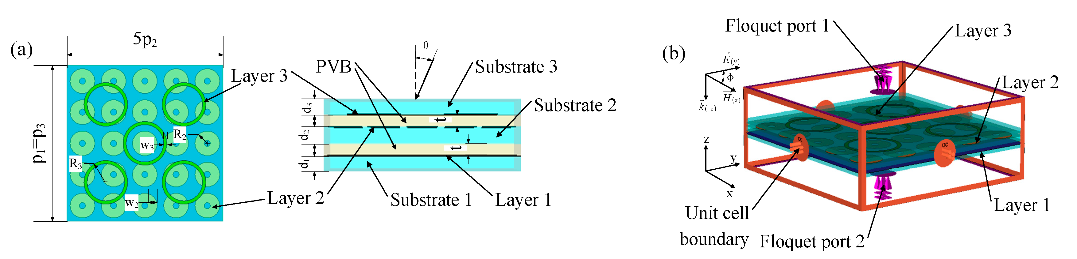
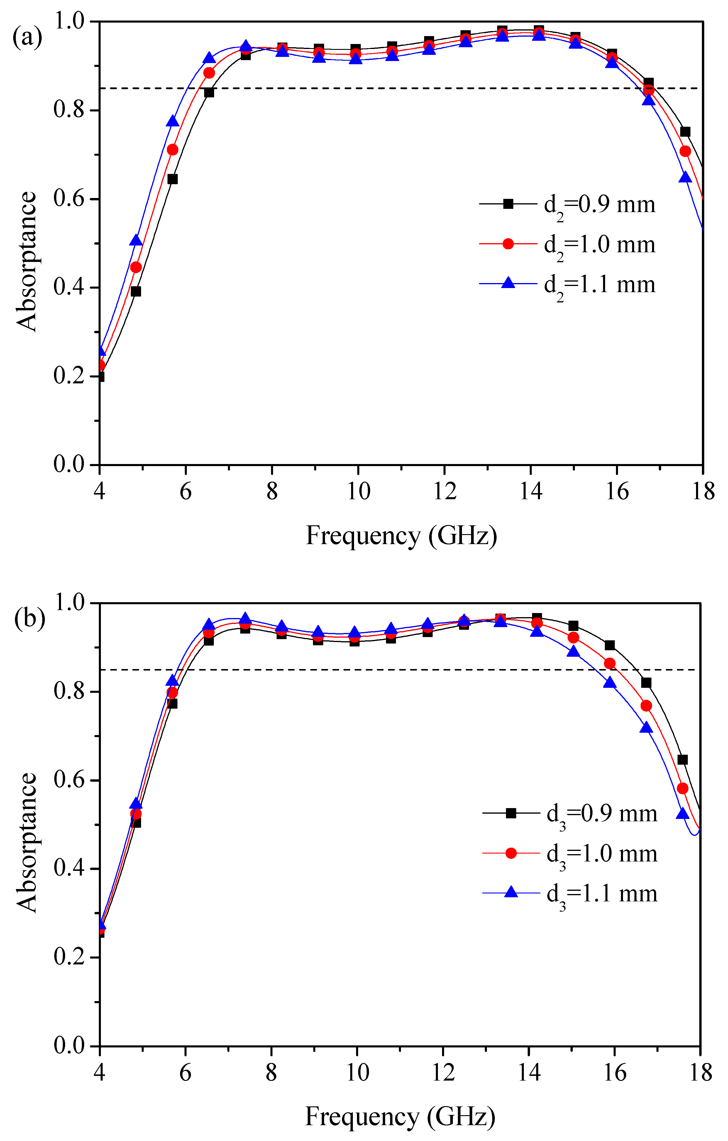
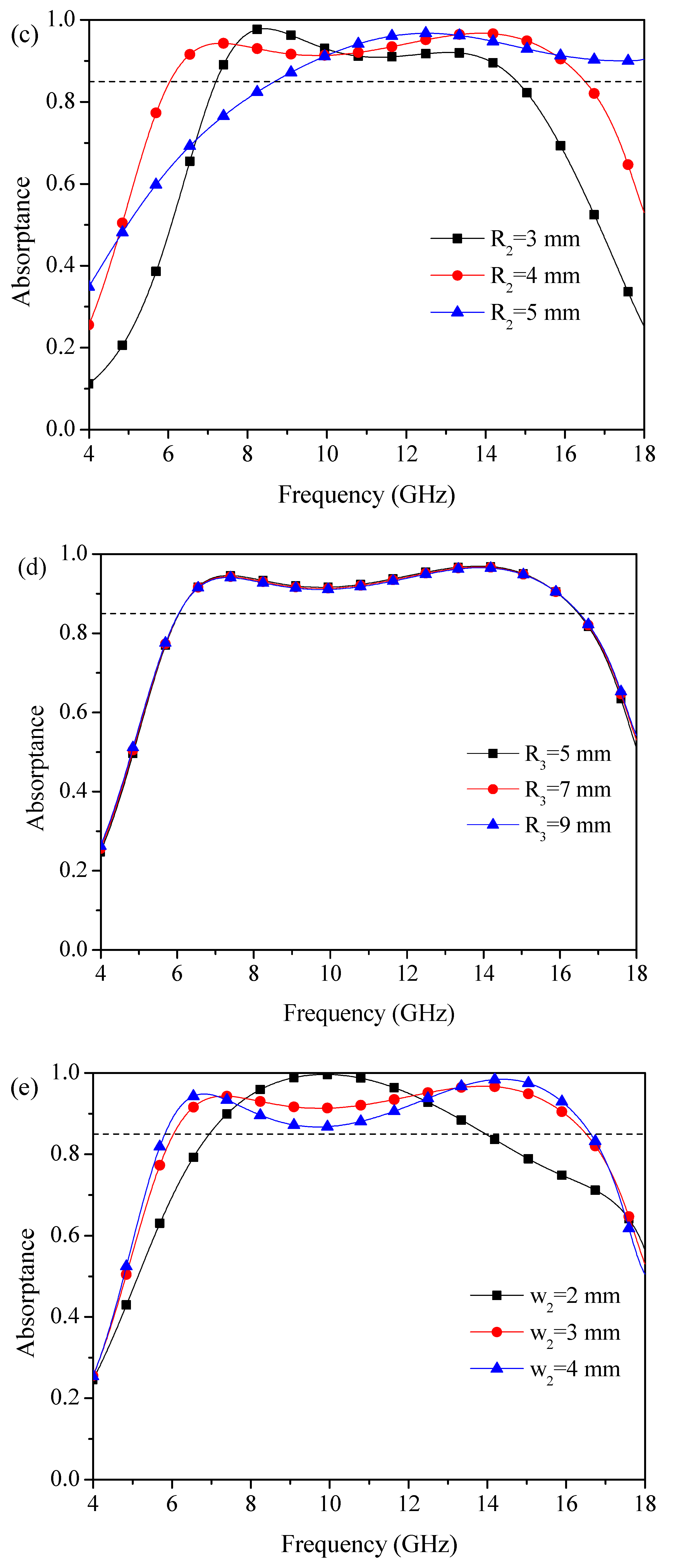
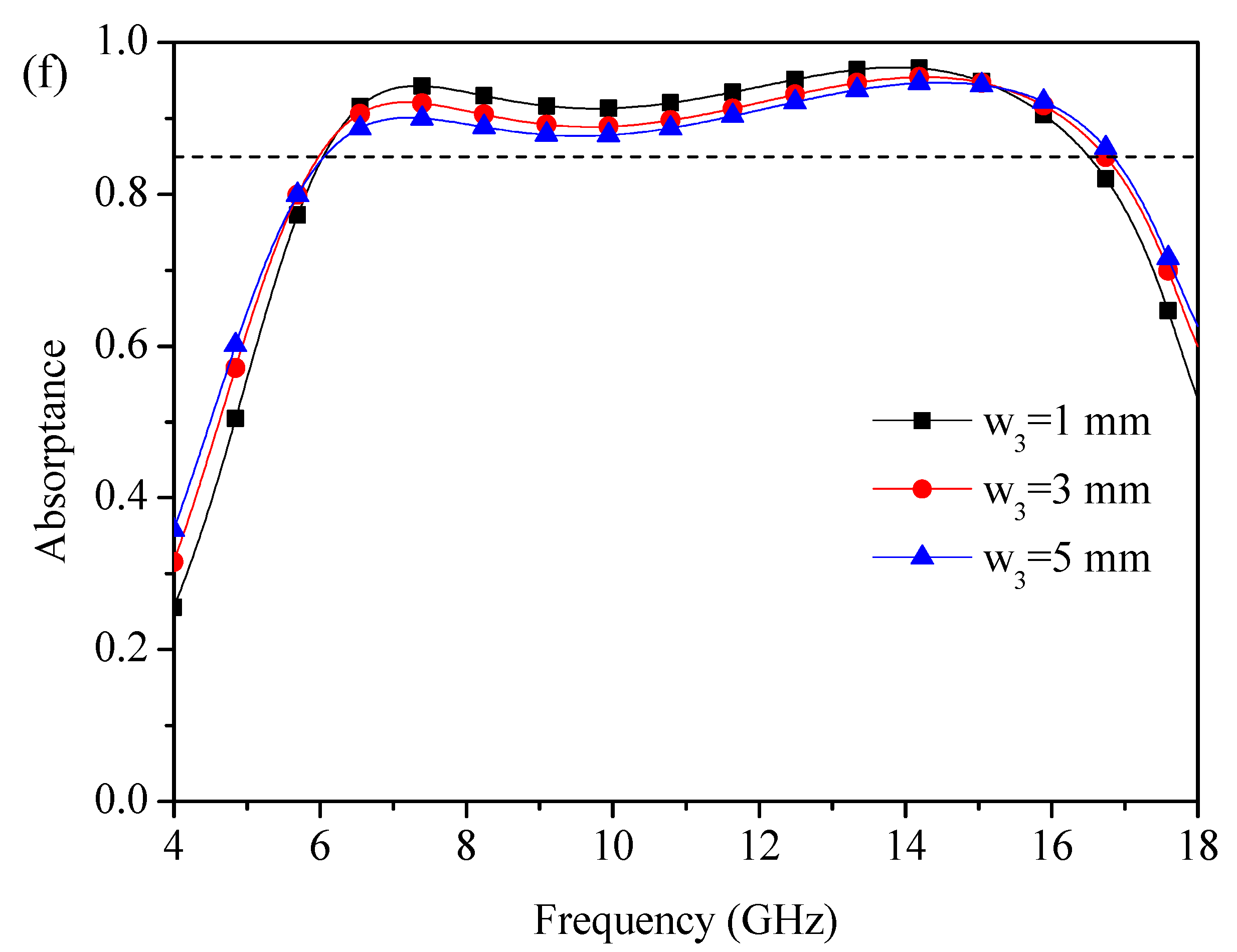
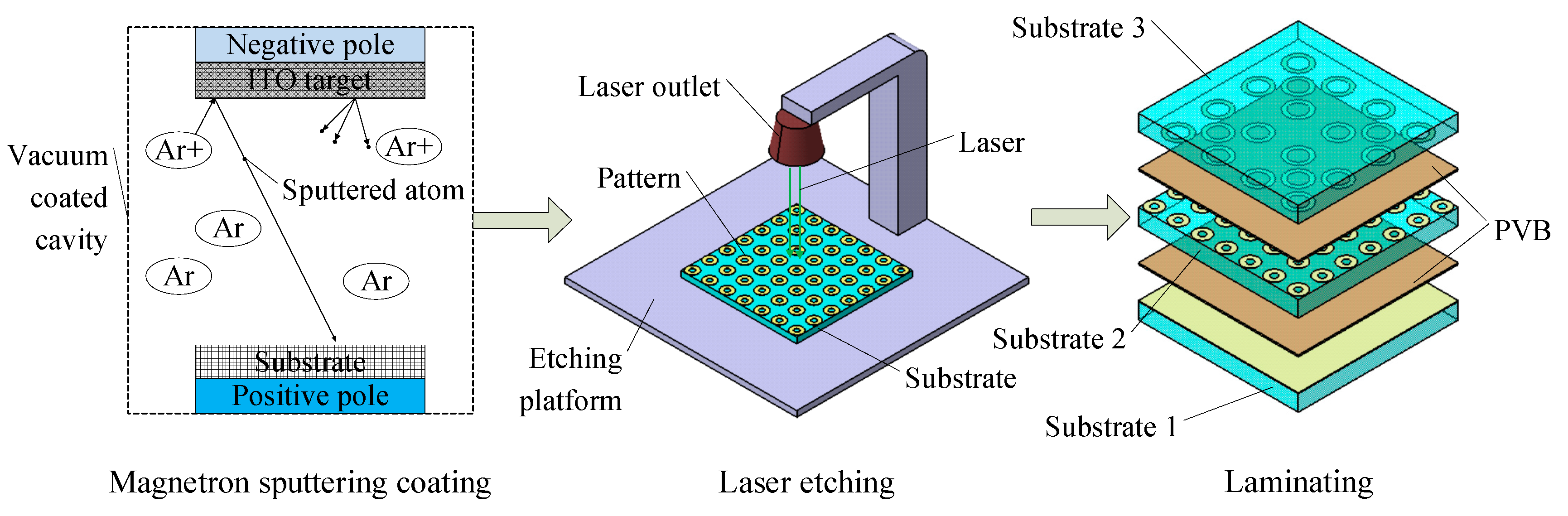
2. Design and Simulation

The structure of the unit cell of the transparent metamaterial absorber is depicted in Figure 1a. The unit cell is composed of three layers of indium tin oxide (ITO), two layers of polyvinyl butyral (PVB) films and three layers of dielectric substrates. In order to improve the transparency of the absorber, we used ultra-white glass as the substrate. The ultra-white glass was low-iron glass with high light transmittance (>91.5%). The relative permittivity of ultra-white glass is ε r = 7.0, and the dielectric loss is negligible. The thicknesses of the three layers of ultra-white glass substrate are d 1 , d 2 and d 3 , respectively. The sheet resistances of the three layers of ITO films we utilized were SR1, SR2 and SR3, respectively. The first layer of ITO was printed on the first substrate to serve as the ground plane. The second layer of ITO on the second substrate was designed as a closed ring with period p2, outer diameter R2 and line width w2. The third layer of ITO on the third substrate was designed as a closed ring with period p3, outer radius R3 and line width w3. The two layers of PVB films were used to bond the three substrates. The relative permittivity of PVB is 2.22. The thickness of the PVB is t = 0.76 mm (selected from commercial standards).
We used full-wave analysis software CST MWS (computer simulation technology microwave studio) to simulate the performance of the absorber. The CST MWS simulation model is shown in Figure 1b. As shown in Figure 1b, the unit cell boundary was used to simulate the infinite periodic element of the transparent absorber. The Floquet ports were used to simulate the incident wave. In order to obtain good microwave absorption performance, we optimized the geometric and physical parameters of the absorber. At the same time, the actual processing conditions were fully considered. The optimized structural parameters of the transparent absorber are shown in Table 1.
The absorptance of the transparent absorber can be calculated by A ( ω ) = 1 T ( ω ) R ( ω ) , where T ( ω ) = | S 21 | 2 is the transmittance, and R ( ω ) = | S 11 | 2 is the reflectance. The simulated reflectance, transmittance and absorptance curves of the proposed absorber under normal incidence of transverse electric (TE) wave, obtained by CST MWS, are presented in Figure 2. As shown in Figure 2, the absorber obtained wideband absorption with an efficiency above 85% over the frequency range from 6.0 to 16.5 GHz, in which the bandwidth with an absorptance higher than 90% ranged from 6.4 to 16.0 GHz, and the relative absorption bandwidth was about 91.4%. In addition, the microwave transmittance of the proposed absorber was close to zero. Thus, it was omitted and the calculation of the absorptivity simplified into the formula: A ( ω ) = 1 R ( ω ) . There were two absorption peaks at 7.3 GHz and 13.9 GHz, and the peak absorptance in each case was 94.2% and 96.7%, respectively.
For insight into the physical mechanism of the proposed absorber, surface current distributions of the absorber under different frequencies were studied in Figure 3. By comparing the surface current distribution of three ITO-resistive metasurfaces at different frequencies, it was found that the intensity of surface currents on the first and second ITO film was stronger than the third ITO film at 7.3 GHz. This indicates that the absorption property is mainly attributed to the first and second ITO film. Layer 1 was used to avoid the transmission of electromagnetic waves, so as to achieve better absorption performance, so the lower resistance was selected. Note that at 13.9 GHz, the surface currents of layer 2 and layer 3 were higher than that of layer 1. In addition, it can be observed that the current flowed in opposite directions on layer 1 and layer 2. Such anti-parallel current flows imply the occurrence of magnetic resonances between layer 1 and layer 2. However, the direction of the current flow between layer 2 and layer 3 was parallel. Such parallel current flows indicate the occurrence of electric resonances between layer 2 and layer 3. Thus, the electric and magnetic resonances occured simultaneously, resulting in a strong broadband absorption.
Furthermore, the power loss, P D , in the unit cell can be calculated by Equation (1).
P D = S R u n i t c e l l | J ( x , y ) | 2 d x d y
where J ( x , y ) is the surface current, and S R is the sheet resistance. Thus, the surface current in the three ITO layers, combined with the ohmic loss from the ITO film, further contribute to the excellent absorption properties. Therefore, the absorption bandwidth and absorptance of the absorber can be precisely adjusted by the geometry and sheet resistance of the ITO metasurface.
In order to further explore this mechanism, the effects of each parameter of the transparent absorber on the absorption property were analyzed. As shown in Figure 4, the absorption response of the proposed absorber under different sheet resistance values of each layer was studied. Note that when the sheet resistance of one layer changed, the sheet resistance of the other two layers remained unchanged. It can be observed from Figure 4a that as the resistance SR1 increased, the first absorption peak intensity slightly decreased, while the second absorption peak intensity stayed pretty much the same. Therefore, changes in SR1 had little impact on absorption performance. The smaller SR1 is, the lower the optical transparency of the absorber is, and the better the shielding effectiveness is. Thus, considering the optical transparency and shielding effect, SR1 = 3 Ω/sq was selected. It can be seen from Figure 4b that with the increase in resistance SR2, the first absorption peak intensity first decreased and then increased, while the second absorption peak intensity decreased. At the same time, the first and second absorption peaks shifted toward each other. Therefore, the absorption bandwidth of the absorber decreased with the increase in SR2. Thus, it is clear that there is an optimal sheet resistance value (SR2 = 45 Ω/sq) for the widest absorption bandwidth (greater than 85%). In this case, the two absorption peaks overlap and together form a continuous broadband absorption of above 85%, ranging from 6.0 to 16.5 GHz. As shown in Figure 4c, the first and second absorption peak intensities slightly increased with the increase in resistance SR3. At the same time, the change in SR3 had little influence on the absorption bandwidth. Considering that ITO is difficult to prepare when its sheet resistance is very high, we chose SR3 = 200 Ω/sq. In conclusion, the absorption performance of the absorber was not sensitive to SR1 and SR3, but sensitive to SR2. Therefore, in preparation, SR2 needs to be strictly controlled, while SR1 and SR3 can be appropriately relaxed.
The influence of the ITO pattern’s geometric dimensions on the absorption property of the absorber was studied, as shown in Figure 5. It is observed from Figure 5 that the absorption performance of the absorber was sensitive to d2, d3, R2, w2 and w3, while it was not sensitive to R3. We selected three types of ultra-white glass thickness (0.9 mm, 1.0 mm, 1.1 mm) based on existing production standards. Since the first layer of substrate is completely covered by ITO, its thickness has no effect on the absorption performance of the absorber. In order to reduce the thickness of the entire absorber, the thickness of the first substrate (d1) was selected to be 0.9 mm. It can be seen from Figure 5a that as d2 increased, the first absorption intensity increased, while the second absorption peak intensity decreased. Meanwhile, the first absorption peaks shifted toward the low-frequency direction, but the position of the second absorption peak was unchanged. Thus, the absorption band broadened. We chose the thickness of the second substrate d2 = 1.1 mm. As d3 increased, the change in absorption peak strength was the same as that in Figure 5a, as shown in Figure 5b. The first and second absorption peaks moved to the left at the same time, but the second absorption peak moved more to the right than the first absorption peak. Therefore, the absorption bandwidth was reduced. We chose the thickness of the third substrate d3 = 0.9 mm. As shown in Figure 5c, the first absorption peak intensity decreased as R2 increased, while the second absorption peak intensity increased. At the same time, the first absorption peak shifted toward the low-frequency direction, but the second absorption peak shifted toward the high-frequency direction. Therefore, the overall absorption bandwidth increased. However, when R2 increased to 5, the first absorption peak strongly shifted to the higher frequencies, and the second one was at 20.9 GHz. At this point, the absorption bandwidth could not cover the entire X-band. Thus, it is apparent that there is an optimum R2 value (R2 = 4 mm) for the widest absorption bandwidth. It can be seen from Figure 5d that as R3 changed, the absorption performance was essentially unchanged. Considering the convenience of processing the sample, we chose R3 = 7 mm. It can be seen from Figure 5e that with the decrease in w2, the intensity of the first and second absorption peaks both decreased. Meanwhile, the first and second absorption peaks moved toward each other, so the absorption bandwidth was reduced. When w2 was reduced to 2 mm, the first and second absorption peaks were superimposed on each other to form an absorption peak. Therefore, there is an optimal w2 value (w2 = 3 mm) to maximize the absorption bandwidth (above 85%). At this point, the two absorption peaks overlap each other to form a continuous broadband absorption of greater than 85%, from 6.0 to 16.5 GHz. Figure 5f shows the impact of w3 on the absorption performance of the absorber. As shown in Figure 5f, the first and second absorption peak intensities both decreased with the increase in w3. At the same time, with the increase in w3, the absorption bandwidth of the absorber increased slightly, but the average absorptance decreased. Therefore, there is an optimal w3 value (w3 = 1 mm) that enables the absorber to have a large average absorptance and absorption bandwidth. In summary, the optimum geometric dimension parameters of the absorber are as follows: d1 = 0.9 mm, d2 = 1.1 mm, d3 = 0.9 mm, R2 = 4 mm, R3 = 7 mm, w2 = 3 mm and w3 = 1 mm.
In many practical applications, it is necessary for the absorber to have good angular stability. The absorptivity of the designed absorber under different oblique incidences of irradiation for both TE and transverse magnetic (TM) modes are depicted in Figure 6. Under TE mode irradiation, the absorption was maintained above 85% at incident angles from 0 to 40°, while the absorption band remained nearly unchanged, as shown in Figure 6a. It can be seen from Figure 6b that the absorptivity was maintained above 85% at incident angles from 0 to 70° for TM mode. By comparing Figure 6a,b, it can be seen that the angular stability of the absorber was better for the TM mode. In general, at TE and TM modes from 0 to 40 degrees of incidence, the absorptivity of the absorber was over 85%, and the operating bandwidth spanned from 6.0 to 16.5 GHz. This indicates that the absorber has a wide incident angle stability.
As shown in Figure 7, the absorptance of the proposed absorber was almost invariable when the polarization angles varied from 0 to 90°. This indicates that the designed absorber has polarization stability, which is attributed to the axisymmetric property of the structure.

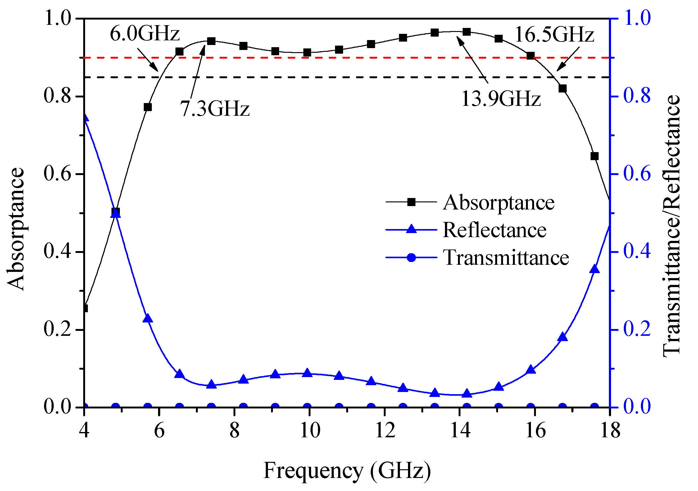
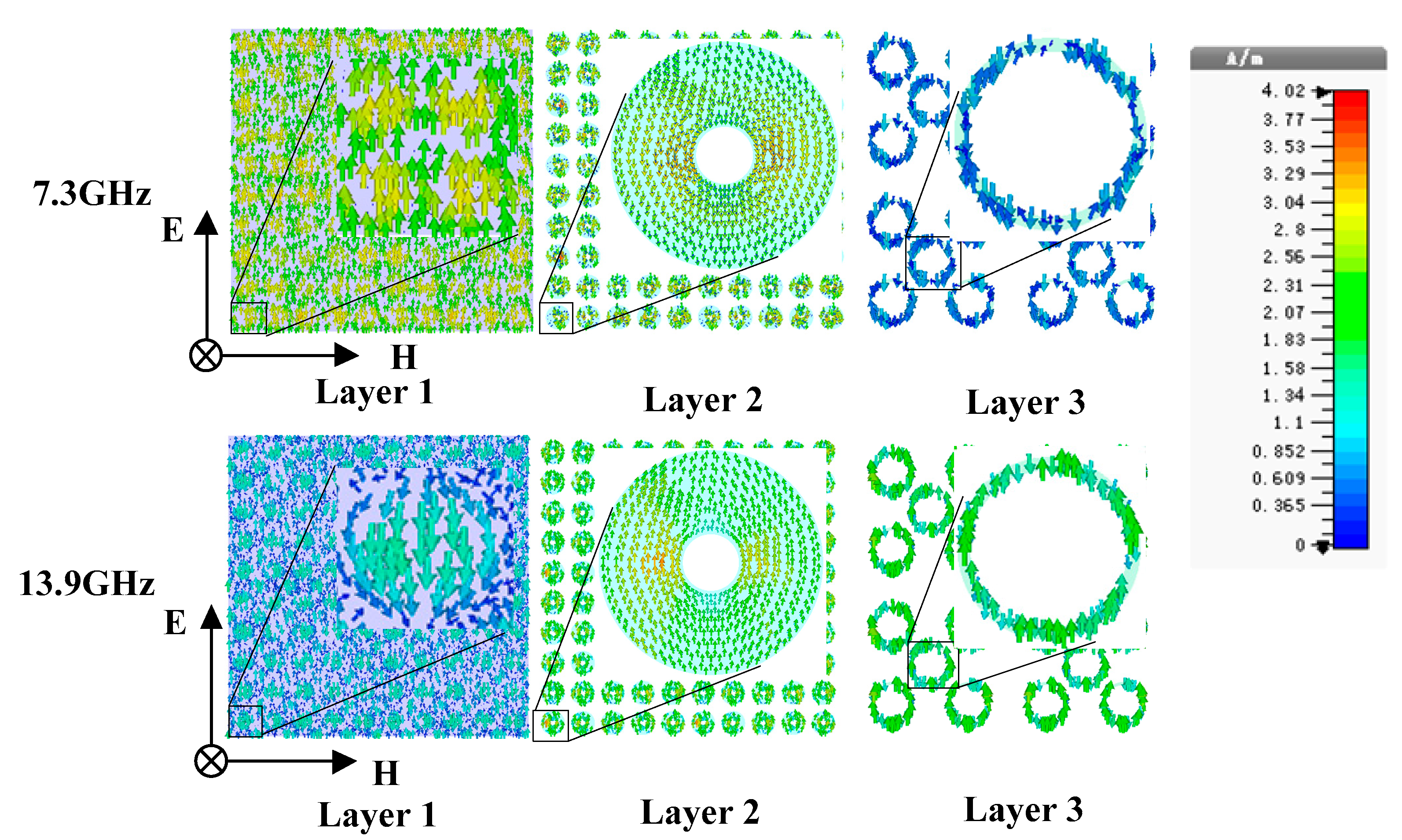
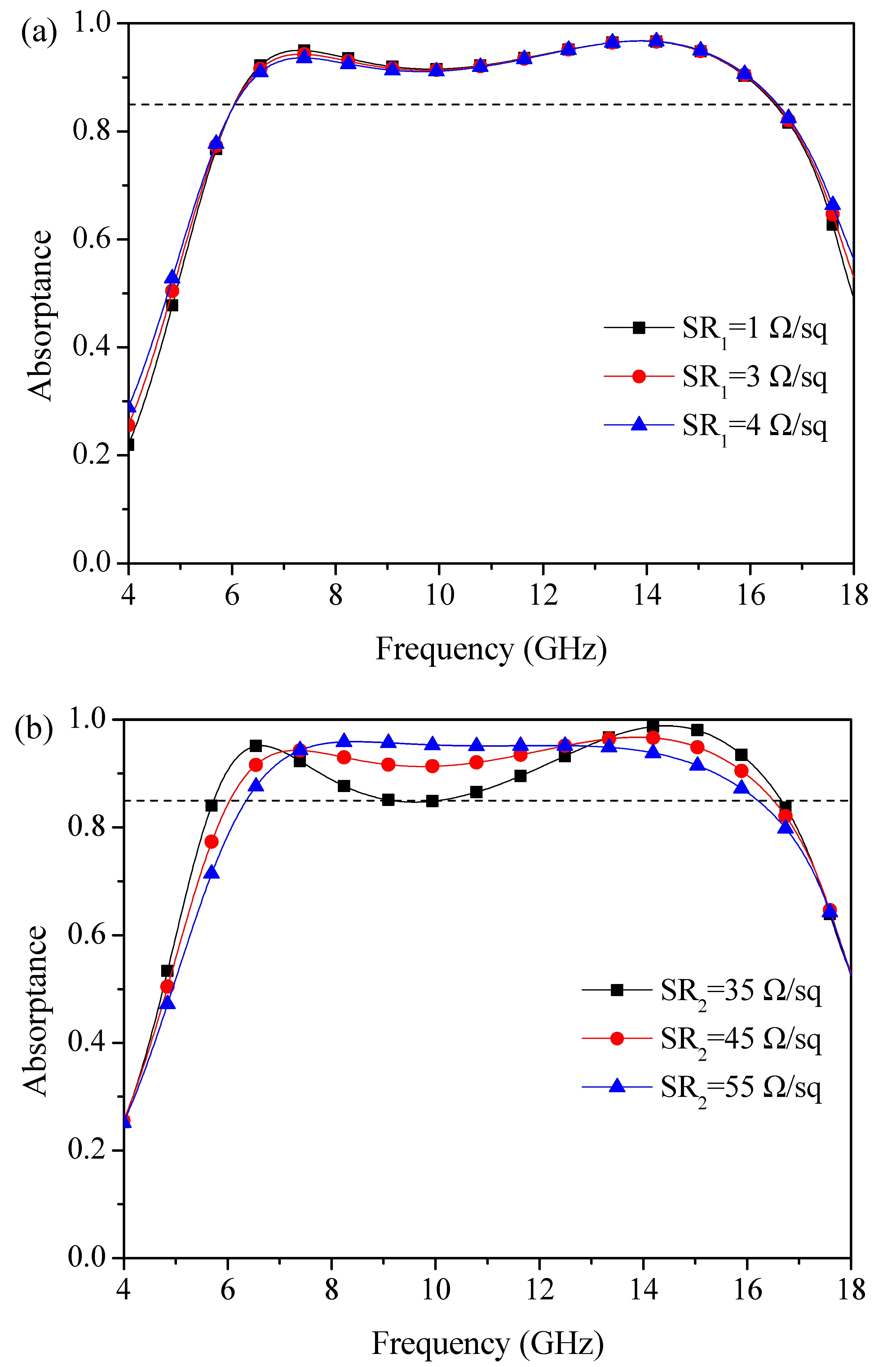
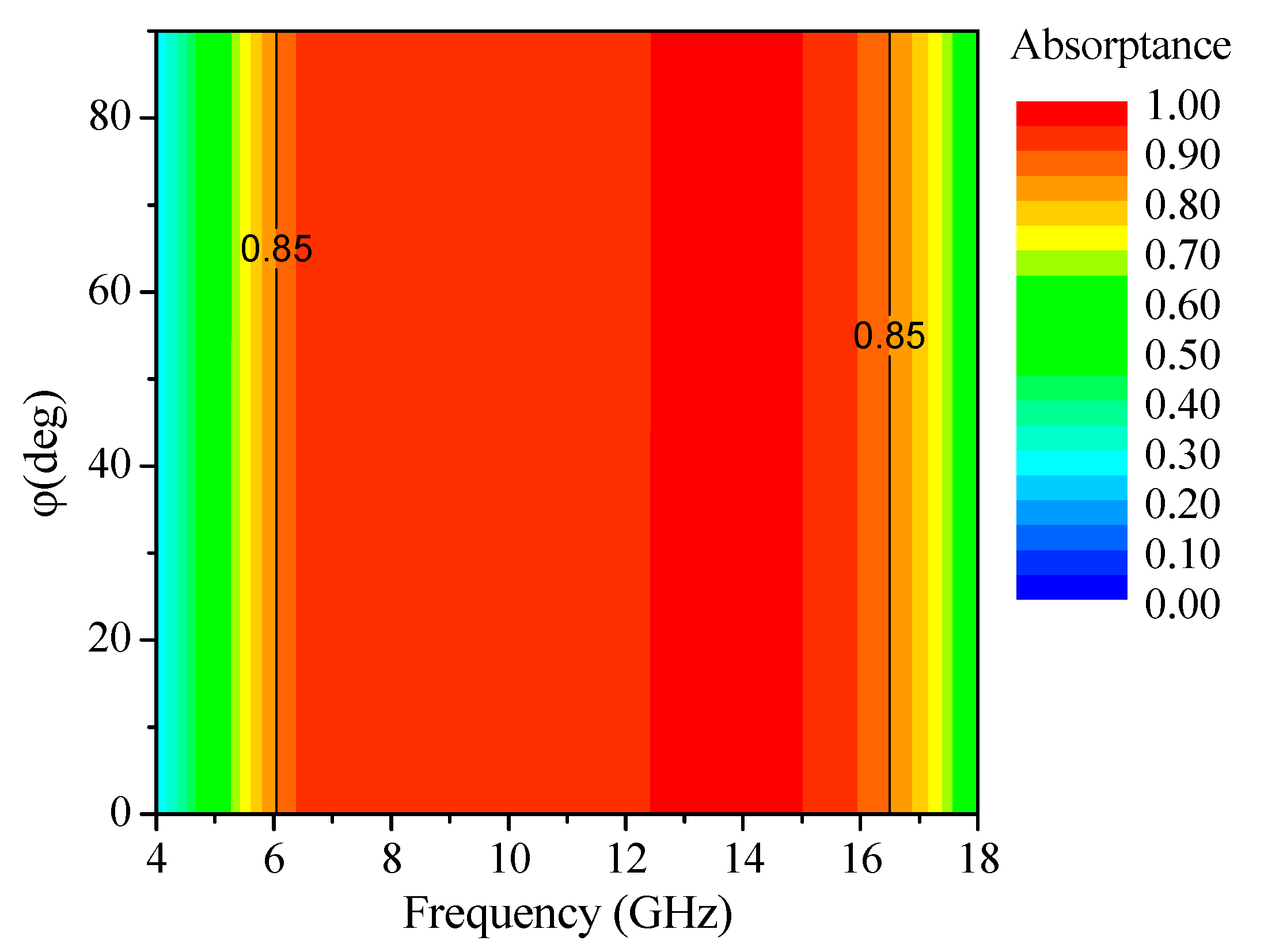
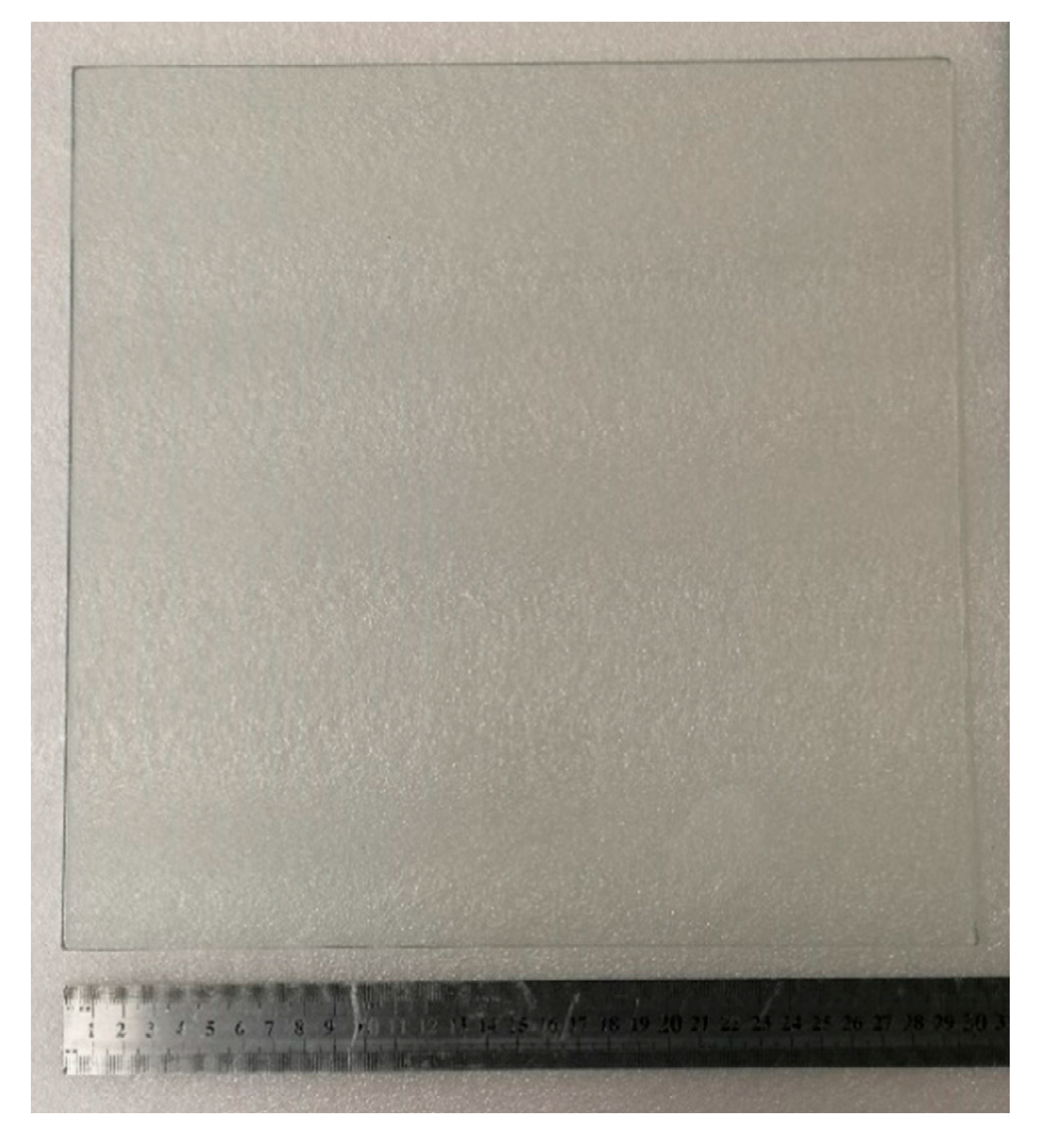
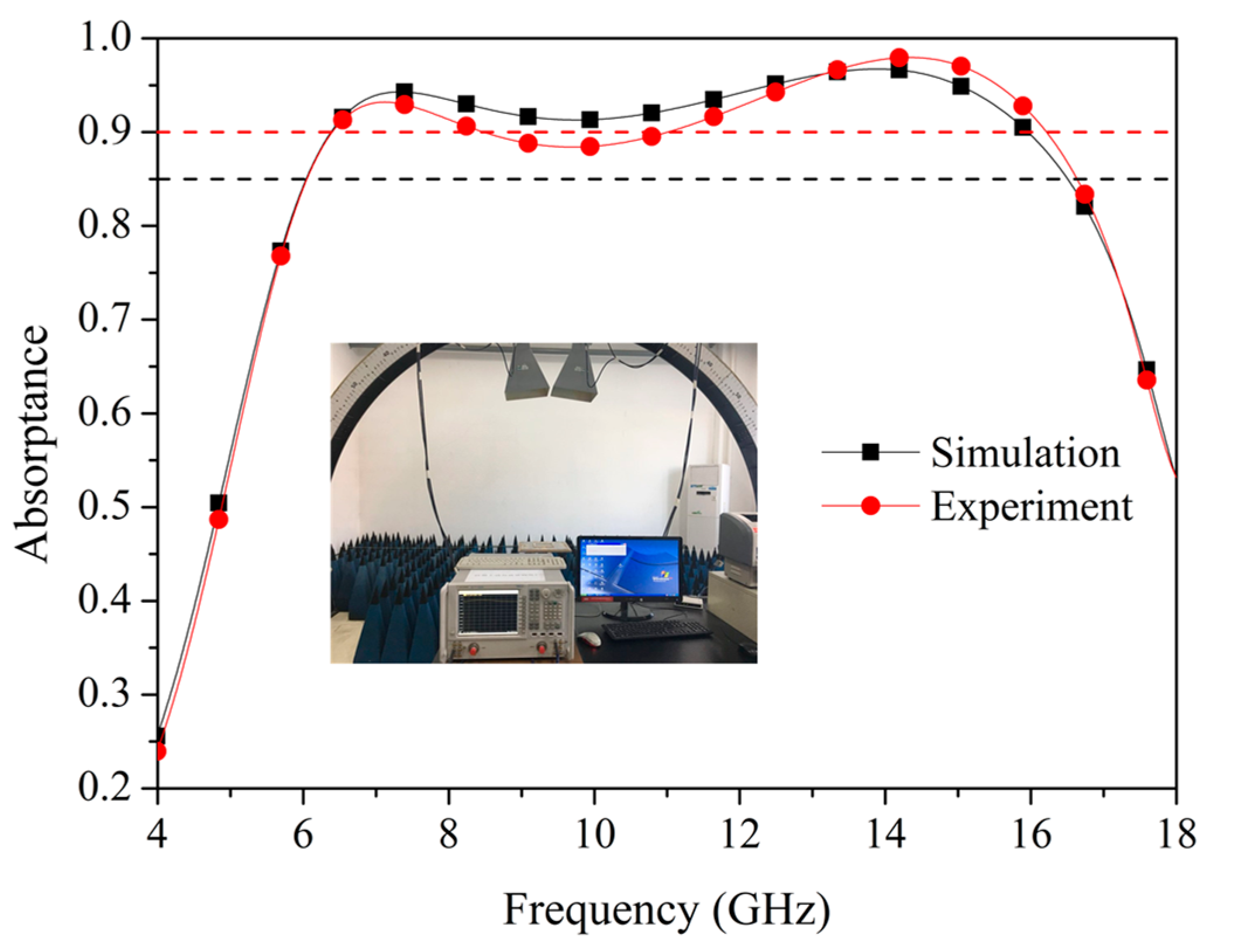
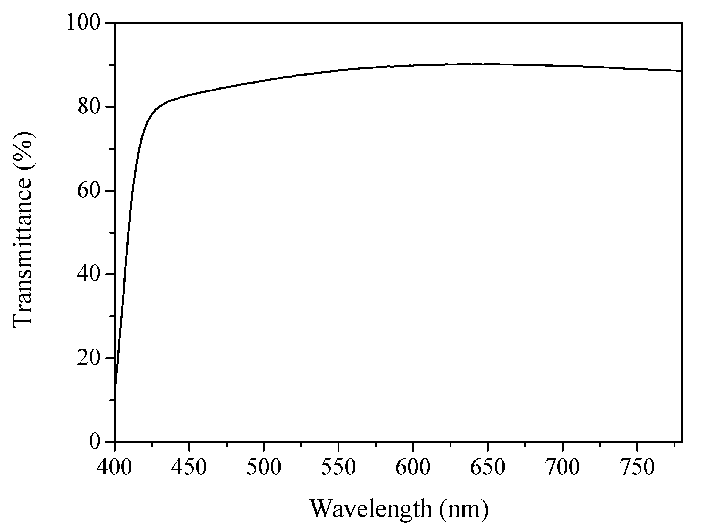
3. Experiment Results

In order to verify the absorption performance of the designed absorber, a 300 mm × 300 mm sample was fabricated, as shown in Figure 8. The production flow chart of the sample is shown in Figure 9. The preparation process was consistent with that described in our previous paper [38]. Firstly, the conductive glass was obtained by coating the ultra-white glass with ITO film by the magnetron sputtering technique. We prepared conductive glass with sheet resistance of 3 Ω/sq, 45 Ω/sq and 200 Ω/sq, respectively. Secondly, the corresponding patterns on the conductive glass were etched by laser-etching technology. Finally, two layers of PVB films were used to combine the three layers of glass into a complete wave-absorbing structure under high temperature and pressure. At the same time, the use of PVB also helped to reduce the profile because PVB reduces the refractive index difference between interfaces. We used an autoclave for this lamination process.
We measured the absorption performance of the transparent absorber by the arch test system. The comparison of the measured and simulated absorptance of the transparent absorber is shown in Figure 10. It can be seen from Figure 10 that the experimental and simulated results are in good agreement. The overall trend of the measured results is consistent with the simulation results. The measured results also have two absorption peaks, at 7.1 GHz and 14.3 GHz respectively. It can be found that the two absorption peaks of the experimental results moved slightly towards low frequency and high frequency, respectively; thus, the absorption bandwidth was slightly increased (6.0~16.7 GHz, absorptance > 85%). At the same time, the experimental values of absorptivity in the absorption band were slightly lower than the simulation results, which was reduced by about 3%. The sheet resistance SR2 of the second ITO layer was non-uniform and less than the optimal value, which may cause this spectral displacement, as shown in Figure 4b. In addition, PVB was used to bond three layers of glass, which resulted in the thickness between the glasses not being precisely controlled, which may also have led to the reduction in the absorption peak. Although there were some deviations between the experimental value and the simulation value, these deviations are within the acceptable range and can be reasonably explained, and the deviations can be reduced by optimizing the process parameters.
The optical transmittance of the fabricated absorber was measured by the Agilent spectrophotometer (Carry5000), as shown in Figure 11. It can be observed that the average transmittance of the transparent absorber in the visible band was approximately 85.7%. Therefore, the absorber designed in this paper proved to have a high transmittance in the visible band. This property can effectively improve the working environment in practical applications.
Finally, the characteristics of the previously reported transparent absorbers are summarized in Table 2. The results show that the proposed absorber not only has a wide absorption band, but also has advantages in relative thickness and visible light transmittance. Therefore, its broadband absorption, high transparency, low profile, polarization insensitivity and oblique incidence stability mean that the proposed transparent absorber has potential use in many practical applications, such as observation windows in communication vehicles, electromagnetic shielding rooms and transparent radio-frequency identification systems.

4. Conclusions

In this paper, an optically transparent metamaterial broadband absorber with high transparence, low profile, polarization insensitiveness and oblique incidence stability is proposed, as confirmed by both the simulation results and the experimental measurements. The thickness of the absorber is only 0.088λ at the lowest cutoff frequency. The measured bandwidth with an absorptance of more than 85% ranges from 6.0 GHz to 16.7 GHz. The measured average optical transmittance is 85.7%. Less thickness can effectively reduce the weight of the absorber, and higher transparency can significantly improve its optical use in practical applications. In addition, all ITO patterns are located inside the structure, which can significantly increase its service life. The proposed transparent absorber has potential utilizations in practical applications in the observation windows in communication vehicles, electromagnetic shielding rooms and transparent radio-frequency identification systems.

Author Contributions

Conceptualization, H.X.; methodology, H.X. and C.W.; validation, R.Q. and C.W.; investigation, R.Q.; writing—original draft preparation, H.X.; writing—review and editing, C.W. and R.Q.; visualization, R.Q.; supervision, M.L.; project administration, M.L. All authors have read and agreed to the published version of the manuscript.

Funding

This research received no external funding.

Conflicts of Interest

The authors declare no conflict of interest.

References

  1. Yin, X.; Long, C.; Li, J.; Zhu, H.; Chen, L.; Guan, J.; Li, X. Ultra-wideband microwave absorber by connecting multiple absorption bands of two different-sized hyperbolic metamaterial waveguide arrays. Sci. Rep.-UK 2015, 5, 15367. [Google Scholar] [CrossRef] [Green Version]
  2. Yang, Z.; Luo, F.; Zhou, W.; Zhu, D.; Huang, Z. Design of a broadband electromagnetic absorbers based on TiO2/Al2O3 ceramic coatings with metamaterial surfaces. J. Alloys Compd. 2016, 687, 384–388. [Google Scholar] [CrossRef]
  3. Zhu, T.; Shen, W.; Wang, X.; Song, Y.-F.; Song, Y.-F. Paramagnetic CoS2@MoS2 core-shell composites coated by reduced graphene oxide as broadband and tunable high-performance microwave absorbers. Chem. Eng. J. 2019, 378, 122159. [Google Scholar] [CrossRef]
  4. Fante, R.L.; McCormack, M.T. Reflection properties of the Salisbury screen. IEEE Trans. Antennas Propag. 1988, 36, 1443–1454. [Google Scholar] [CrossRef]
  5. Chambers, B. Optimum design of a Salisbury screen radar absorber. Electron. Lett. 1994, 30, 1353–1354. [Google Scholar] [CrossRef]
  6. Toit, L.J.D. The design of Jauman absorbers. IEEE Antennas Propag. Mag. 1994, 36, 17–25. [Google Scholar] [CrossRef]
  7. Du Toit, L.J.; Cloete, J.H. Electric screen Jauman absorber design algorithms. IEEE Trans. Microw. Theory Tech. 1996, 44, 2238–2245. [Google Scholar] [CrossRef]
  8. Landy, N.I.; Sajuyigbe, S.; Mock, J.J.; Smith, D.R.; Padilla, W.J. Perfect metamaterial absorber. Phys. Rev. Lett. 2008, 100, 207402. [Google Scholar] [CrossRef]
  9. Gogoi, D.J.; Bhattacharyya, N.S. Metasurface absorber based on water meta “molecule” for X-band microwave absorption. J. Appl. Phys. 2018, 124, 075106. [Google Scholar] [CrossRef]
  10. Yahiaoui, R.; Tan, S.; Cong, L.; Singh, R.; Yan, F.; Zhang, W. Poisson distributions in disordered metamaterials absorbers. J. Appl. Phys. 2019, 125, 213106. [Google Scholar]
  11. Yahiaoui, R.; Tan, S.; Cong, L.; Singh, R.; Yan, F.; Zhang, W. Multispectral terahertz sensing with highly flexible ultrathin metamaterial absorber. J. Appl. Phys. 2015, 118, 083103. [Google Scholar] [CrossRef]
  12. Cheng, Y.; Zou, Y.; Luo, H.; Chen, F.; Mao, X. Compact Ultra-Thin Seven-Band Microwave Metamaterial Absorber Based on a Single Resonator Structure. J. Electron. Mater. 2019, 48, 3939–3946. [Google Scholar] [CrossRef]
  13. Zhao, J.C.; Cheng, Y.Z. Ultrabroadband Microwave Metamaterial Absorber Based on Electric SRR Loaded with Lumped Resistors. J. Electron. Mater. 2016, 45, 5033–5039. [Google Scholar] [CrossRef]
  14. Yahiaoui, R.; Ouslimani, H.H. Broadband polarization-independent wide-angle and reconfigurable phase transition hybrid metamaterial absorber. J. Appl. Phys. 2017, 122, 093104. [Google Scholar] [CrossRef]
  15. Beeharry, T.; Yahiaoui, R.; Selemani, K.; Ouslimani, H.H. A Co-Polarization Broadband Radar Absorber for RCS Reduction. Materials 2018, 11, 1668. [Google Scholar] [CrossRef] [PubMed] [Green Version]
  16. Tao, H.; Bingham, C.M.; Strikwerda, A.C.; Pilon, D.; Shrekenhamer, D.; Landy, N.I.; Fan, K.; Zhang, X.; Padilla, W.J.; Averitt, R.D. Highly flexible wide angle of incidence terahertz metamaterial absorber: Design, fabrication, and characterization. Phys. Rev. B 2008, 78, 241103. [Google Scholar] [CrossRef]
  17. Avitzour, Y.; Urzhumov, Y.A.; Shvets, G. Wide-angle infrared absorber based on a negative-index plasmonic metamaterial. Phys. Rev. B 2009, 79, 045131. [Google Scholar] [CrossRef] [Green Version]
  18. Ding, F.; Cui, Y.; Ge, X.; Jin, Y.; He, S. Ultra-broadband microwave metamaterial absorber. Appl. Phys. Lett. 2012, 100, 103506. [Google Scholar] [CrossRef] [Green Version]
  19. Wei, J.; He, Y.; Bie, S.; Wu, S.; Lei, Z.; Deng, W.; Liu, Y.; Zhang, Y.; Li, C.; Ai, J.; et al. Flexible design and realization of wideband microwave absorber with double-layered resistor loaded FSS. J. Phys. D Appl. Phys. 2019, 52, 185101. [Google Scholar] [CrossRef]
  20. Zhang, H.-F.; Liu, J.-X.; Yang, J.; Zhang, H.; Li, H.-M. A polarization-insensitive broadband terahertz absorber with a multilayer structure. Results Phys. 2018, 11, 1064–1074. [Google Scholar] [CrossRef]
  21. Jiao, X.-F.; Zhang, Z.-H.; Li, T.; Xu, Y.; Song, G.-F. Tunable Dual Broadband Terahertz Metamaterial Absorber Based on Vanadium Dioxide. Appl. Sci. 2020, 10, 7259. [Google Scholar] [CrossRef]
  22. Jiang, X.; Zhang, Z.; Wen, K.; Li, G.; He, J.; Yang, J. A Triple-Band Hybridization Coherent Perfect Absorber Based on Graphene Metamaterial. Appl. Sci. 2020, 10, 1750. [Google Scholar] [CrossRef] [Green Version]
  23. Patel, S.K.; Charola, S.; Parmar, J.; Ladumor, M. Broadband metasurface solar absorber in the visible and near-infrared region. Mater. Res. Express 2019, 6, 086213. [Google Scholar] [CrossRef]
  24. Li, Z.; Stan, L.; Czaplewski, D.A.; Yang, X.; Gao, J. Broadband infrared binary-pattern metasurface absorbers with micro-genetic algorithm optimization. Opt. Lett. 2019, 44, 114–117. [Google Scholar] [CrossRef] [PubMed]
  25. Lan, G.; Jin, Z.; Nong, J.; Luo, P.; Guo, C.; Shang, Z.; Dong, L.; Wei, W. Narrowband Perfect Absorber Based on Dielectric-Metal Metasurface for Surface-Enhanced Infrared Sensing. Appl. Sci. 2020, 10, 2295. [Google Scholar] [CrossRef] [Green Version]
  26. Zhang, Y.; Lv, J.; Que, L.; Mi, G.; Zhou, Y.; Jiang, Y. A visible-infrared double band photodetector absorber. Results Phys. 2020, 18, 103283. [Google Scholar] [CrossRef]
  27. Zhang, H.; Li, Y.; Long, X.; Luo, J.; Zhang, Y.; Song, M.; Fang, J.; Guan, C.; Cheng, Y.; Liu, H. Self-assembled metamaterial perfect absorbers at visible wavelengths using core-shell Au@SiO2meta-atoms. J. Mater. Chem. C 2020, 8, 12876–12885. [Google Scholar] [CrossRef]
  28. Sheokand, H.; Ghosh, S.; Singh, G.; Saikia, M.; Srivastava, K.V.; Ramkumar, J.; Ramakrishna, S.A. Transparent broadband metamaterial absorber based on resistive films. J. Appl. Phys. 2017, 122, 105105. [Google Scholar] [CrossRef]
  29. Wu, Y.; Wang, J.; Lai, S.; Zhu, X.; Gu, W. A transparent and flexible microwave absorber covering the whole WiFi waveband. AIP Adv. 2019, 9, 025309. [Google Scholar] [CrossRef] [Green Version]
  30. Lai, S.; Wu, Y.; Zhu, X.; Gu, W.; Wu, W. An Optically Transparent Ultrabroadband Microwave Absorber. IEEE Photonics J. 2017, 9, 1–10. [Google Scholar] [CrossRef]
  31. Okano, Y.; Ogino, S.; Ishikawa, K. Development of Optically Transparent Ultrathin Microwave Absorber for Ultrahigh-Frequency RF Identification System. IEEE Trans. Microw. Theory Tech. 2012, 60, 2456–2464. [Google Scholar] [CrossRef]
  32. Ryu, Y.H.; Kim, S.S. Design and Fabrication of Metamaterial Absorbers Used for RF-ID. Korean J. Met. Mater. 2020, 58, 131–136. [Google Scholar] [CrossRef]
  33. Aslam, B.; Kashif, M.; Azam, M.A.; Amin, Y.; Loo, J.; Tenhunen, H. A low profile miniature RFID tag antenna dedicated to IoT applications. Electromagnetics 2019, 39, 393–406. [Google Scholar] [CrossRef]
  34. Kurihara, H.; Hirai, Y.; Takizawa, K.; Iwata, T.; Hashimoto, O. An improvement of communication environment for ETC system by using transparent EM wave absorber. IEICE Trans. Electron. 2005, E88C, 2350–2357. [Google Scholar] [CrossRef]
  35. Kulkarni, G.; Kandesar, P.; Velhal, N.; Phadtare, V.; Jatratkar, A.; Shinde, S.; Kim, D.-Y.; Puri, V. Exceptional electromagnetic interference shielding and microwave absorption properties of room temperature synthesized polythiophene thin films with double negative characteristics (DNG) in the Ku-band region. Chem. Eng. J. 2019, 355, 196–207. [Google Scholar] [CrossRef]
  36. Min, P.; Song, Z.; Yang, L.; Dai, B.; Zhu, J. Transparent ultrawideband absorber based on simple patterned resistive metasurface with three resonant modes. Opt. Express 2020, 28, 19518–19530. [Google Scholar] [CrossRef]
  37. Hu, D.; Cao, J.; Li, W.; Zhang, C.; Wu, T.; Li, Q.; Chen, Z.; Wang, Y.; Guan, J. Optically Transparent Broadband Microwave Absorption Metamaterial By Standing-Up Closed-Ring Resonators. Adv. Opt. Mater. 2017, 5, 1700109. [Google Scholar] [CrossRef]
  38. Xiao, H.; Qu, Z.; Lv, M.; Du, H.; Zhu, W.; Wang, C.; Qin, R. Optically transparent broadband and polarization insensitive microwave metamaterial absorber. J. Appl. Phys. 2019, 126, 135107. [Google Scholar] [CrossRef]
  39. Jang, T.; Youn, H.; Shin, Y.J.; Guo, L.J. Transparent and Flexible Polarization-Independent Microwave Broadband Absorber. ACS Photonics 2014, 1, 279–284. [Google Scholar] [CrossRef]
  40. Grande, M.; Bianco, G.V.; Vincenti, M.A.; De Ceglia, D.; Capezzuto, P.; Petruzzelli, V.; Scalora, M.; Bruno, G.; D’Orazio, A. Optically transparent microwave screens based on engineered graphene layers. Opt. Express 2016, 24, 22788–22795. [Google Scholar] [CrossRef] [Green Version]
  41. Yi, D.; Wei, X.C.; Xu, Y.L. Transparent Microwave Absorber Based on Patterned Graphene: Design, Measurement, and Enhancement. IEEE Trans. Nanotechnol. 2017, 16, 484–490. [Google Scholar] [CrossRef]
Figure 1. The structure of the absorber and the CST MWS simulation model. (a) The structure, (b) the CST MWS simulation model.
Applsci 10 09125 g001
Figure 2. The characteristics of the proposed absorber.
Applsci 10 09125 g002
Figure 3. The distributions of surface currents under normally incident TE waves at 7.3 GHz and 13.9 GHz.
Applsci 10 09125 g003
Figure 4. Absorption performance of the absorber for different sheet resistances of the ITO layers: (a) varied SR1; (b) varied SR2; (c) varied SR3.
Applsci 10 09125 g004aApplsci 10 09125 g004b
Figure 5. Absorption performance of the absorber for different geometric dimensions: (a) varied d2; (b) varied d3; (c) varied R2; (d) varied R3; (e) varied w2; (f) varied w3.
Applsci 10 09125 g005aApplsci 10 09125 g005bApplsci 10 09125 g005c
Figure 6. Absorption performance under different incident angles θ , for (a) TE and (b) TM polarizations.
Applsci 10 09125 g006
Figure 7. Absorption performance at different polarization angles φ .
Applsci 10 09125 g007
Figure 8. Photograph of the fabricated absorber sample.
Applsci 10 09125 g008
Figure 9. The production flow chart of the sample.
Applsci 10 09125 g009
Figure 10. Comparison of measured and simulated absorptance of the absorber.
Applsci 10 09125 g010
Figure 11. The measured optical transmittance of the fabricated absorber.
Applsci 10 09125 g011
Table 1. The optimized structural parameters of the absorber.
ParameterValueParameterValue
p150 mmd30.9 mm
p210 mmw23 mm
p350 mmw31 mm
R24 mmt0.76 mm
R37 mmSR13 Ω/sq
d10.9 mmSR245 Ω/sq
d21.1 mmSR3200 Ω/sq
Table 2. Comparison with other transparent broadband absorbers.
AbsorberAbsorption Band above 85% (GHz)Relative Bandwidth 1Thickness (mm)Relative Thickness 2Optical Transmittance
Ref. [39]3.6~19.45.398.60.10362~75%
Ref. [40]8.6~111.283.60.10380~85%
Ref. [41] 12~14.31.197.750.31073~82%
Ref. [37]5.5~19.73.585.50.10182%
Ref. [38]4.6~183.916.760.10475%
This work6.0~16.72.784.420.08885.7%
1 Relative bandwidth is defined as the ratio of the highest frequency and the lowest frequency in the band when absorption is better than 85%; 2 Relative thickness is defined as the ratio of the thickness and wavelength of the lowest absorption frequency when absorption is better than 85%.
Publisher’s Note: MDPI stays neutral with regard to jurisdictional claims in published maps and institutional affiliations.

