
A Review on Ultrafast Laser Microwelding of Transparent Materials and Transparent Material–Metals
 ,
,
Abstract
:1. Introduction
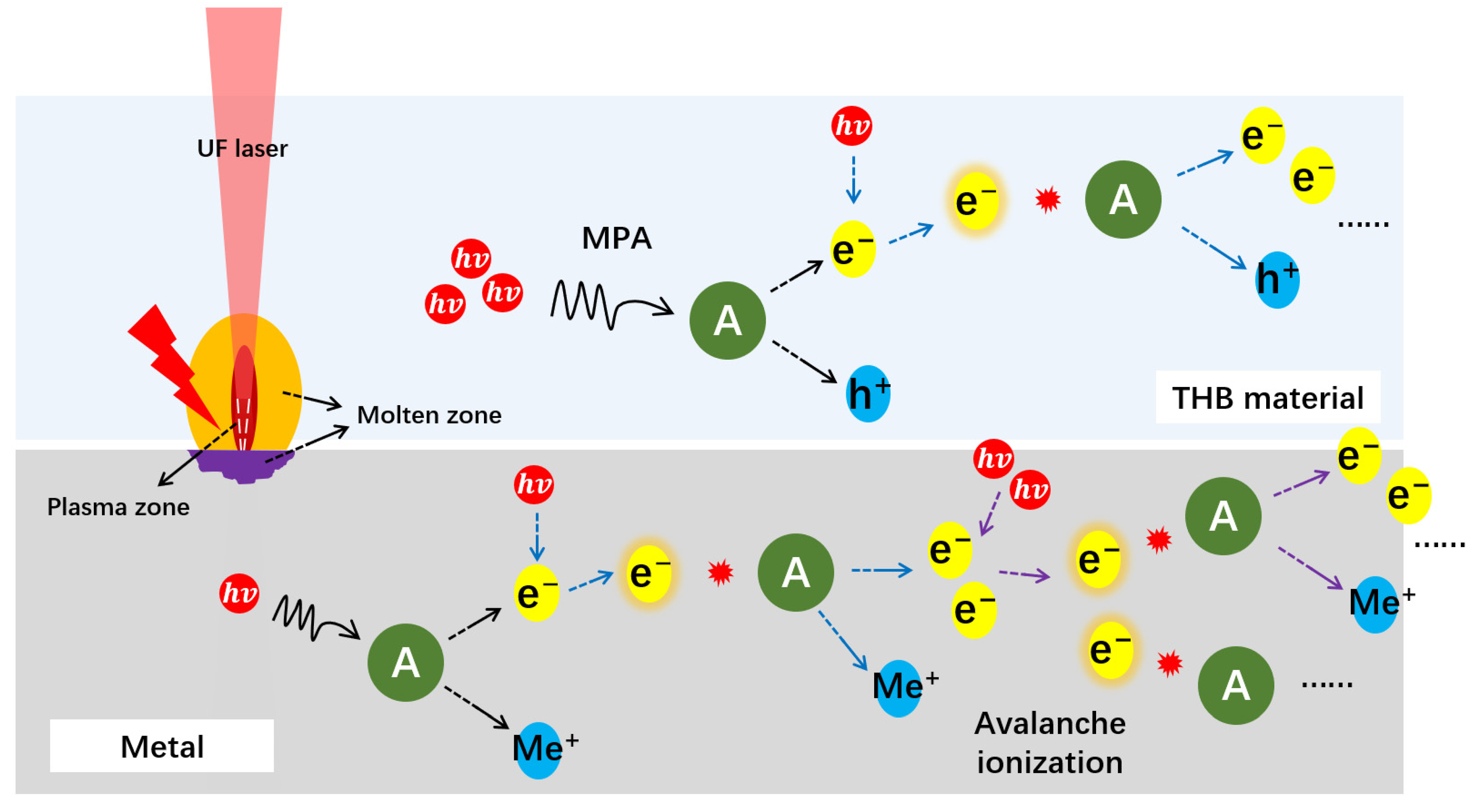
2. Mechanisms of Ultrafast Laser Microwelding
3. Advances in Ultrafast Laser Microwelding of THB Materials and THB Material–Metals
3.1. THB Material Microwelding
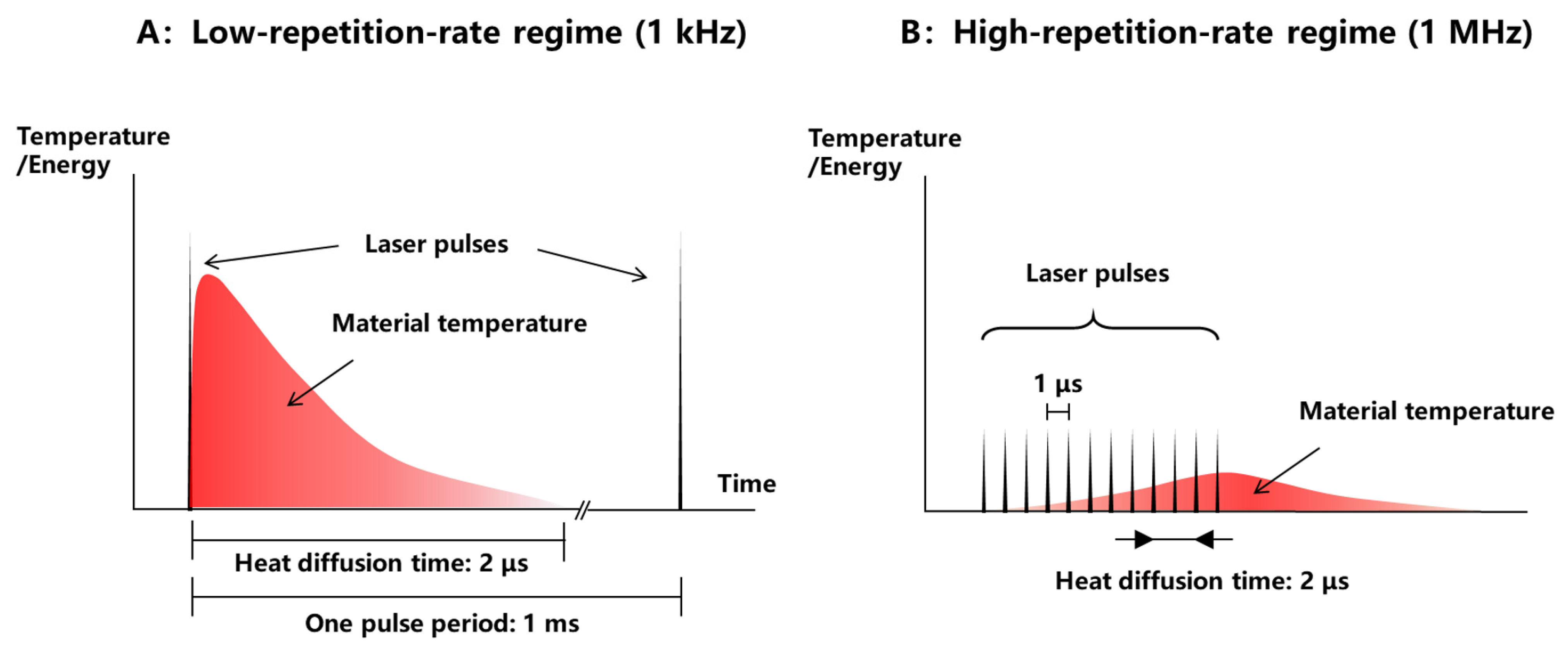
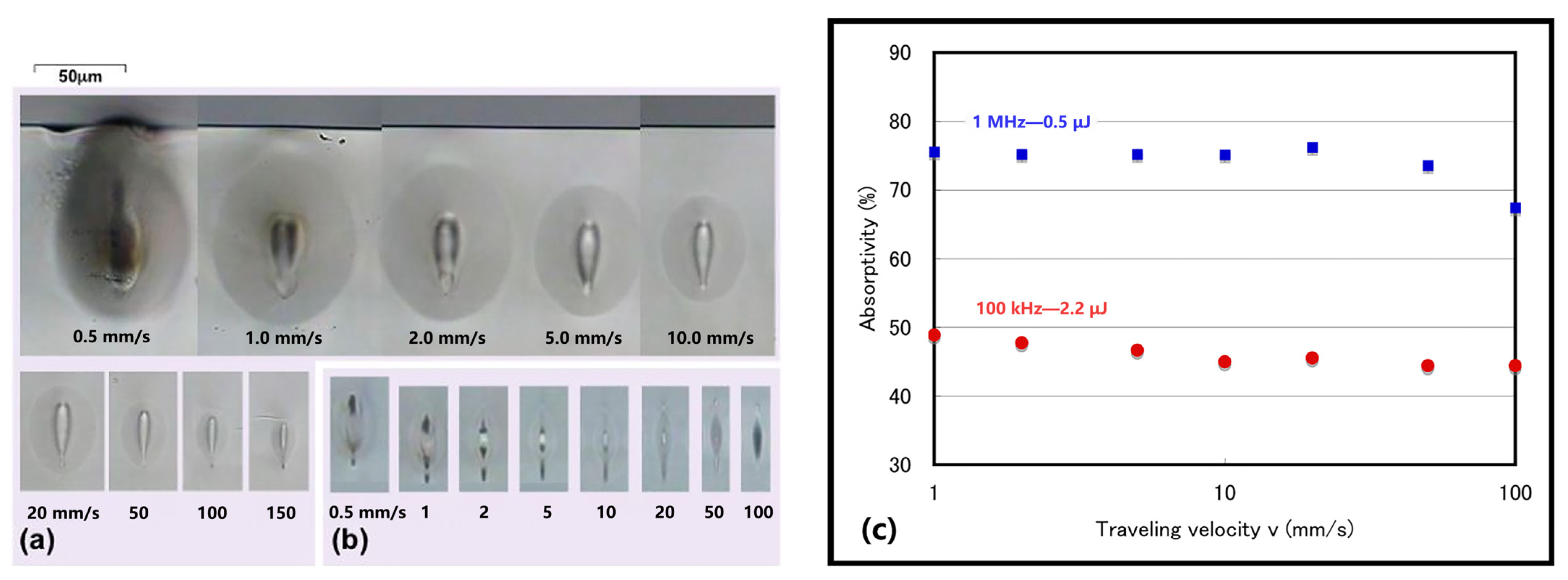
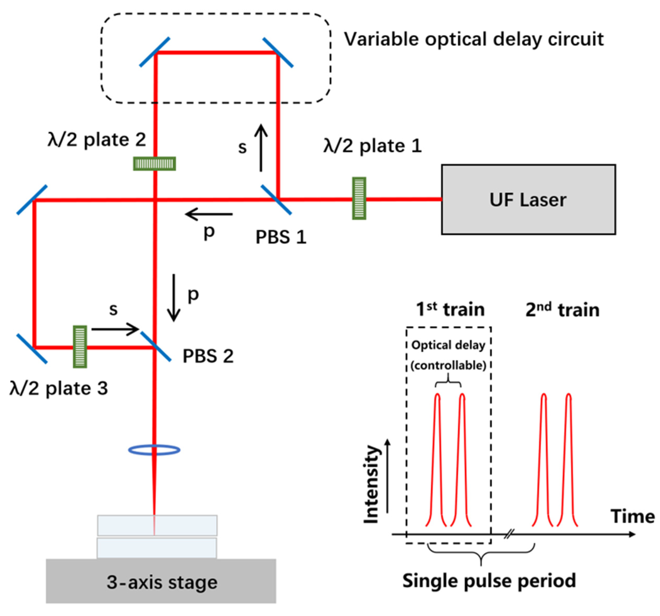
3.1.1. Pulse Repetition Frequency
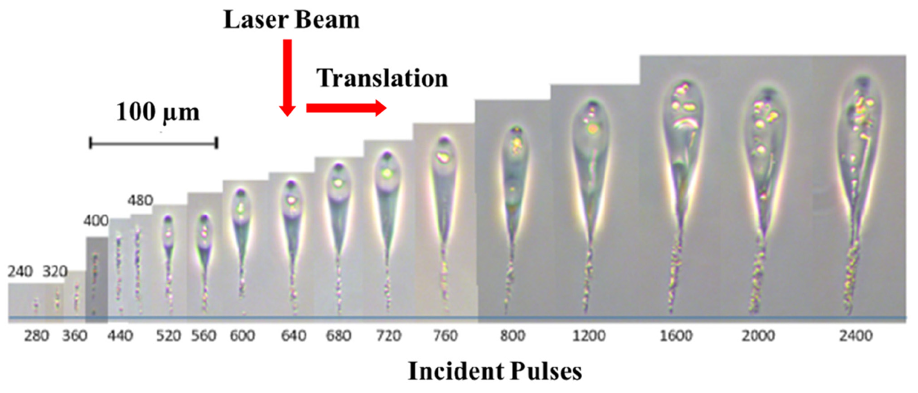
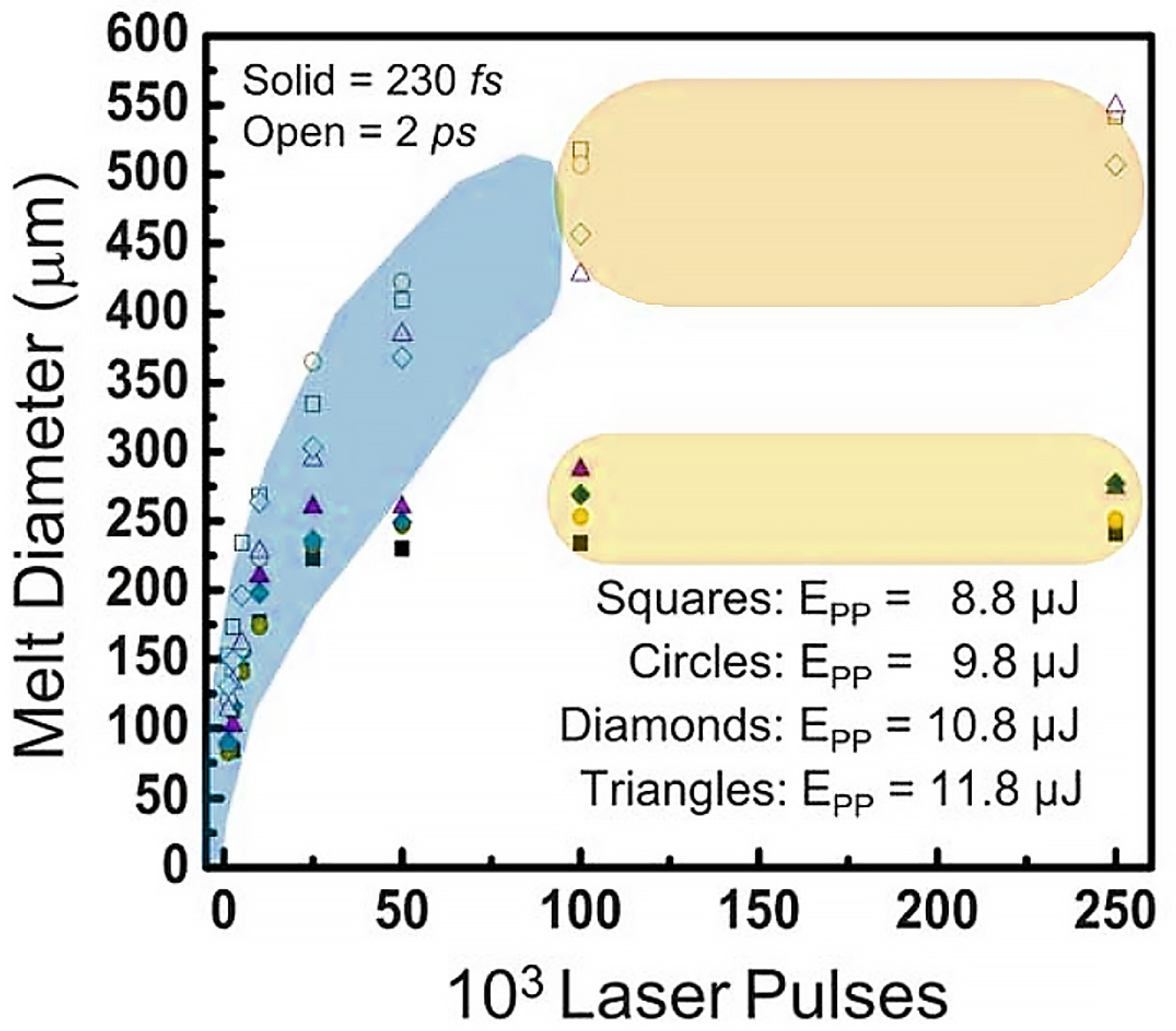
3.1.2. Pulse Number
3.1.3. Pulse Duration
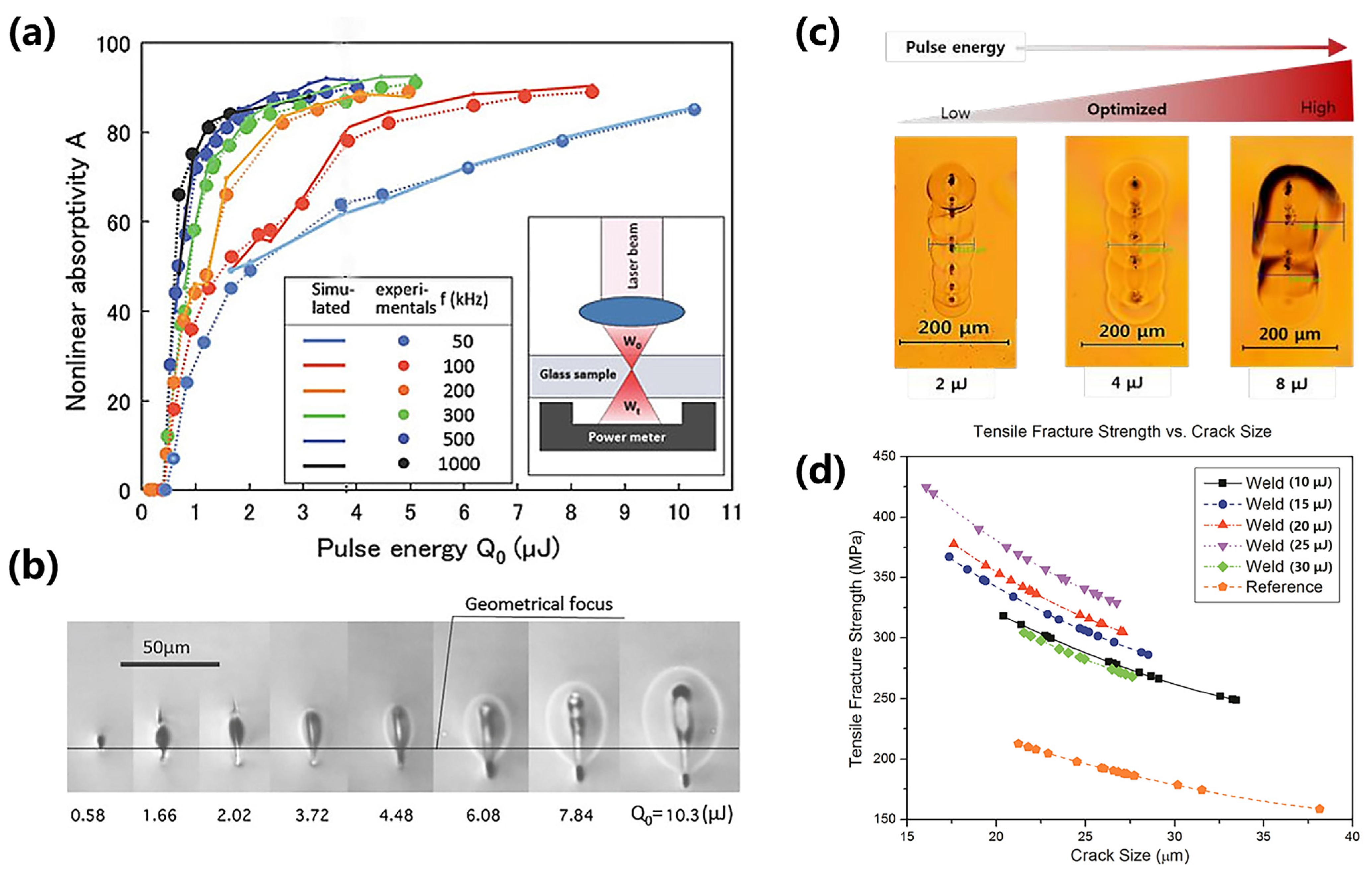
3.1.4. Pulse Energy
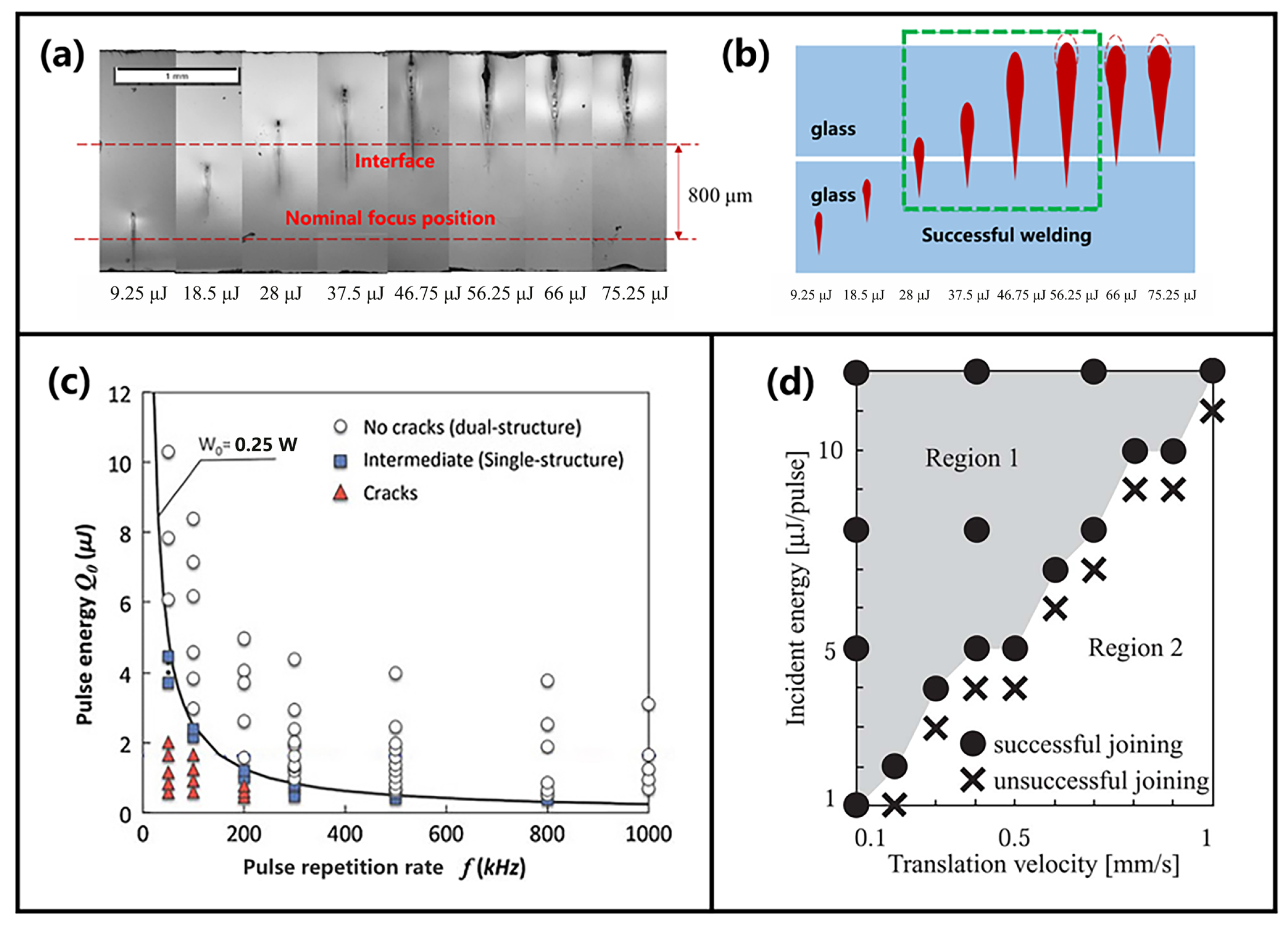
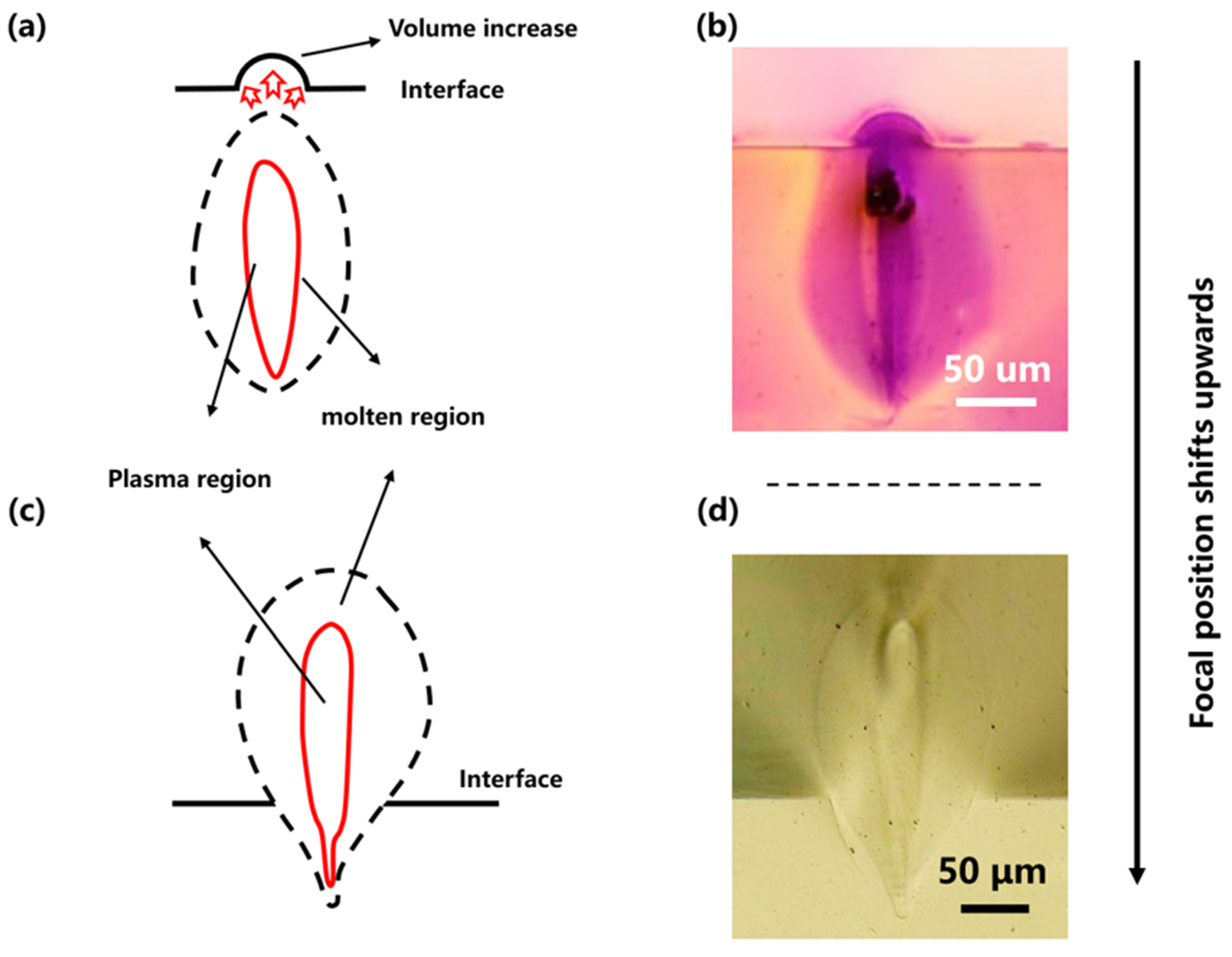
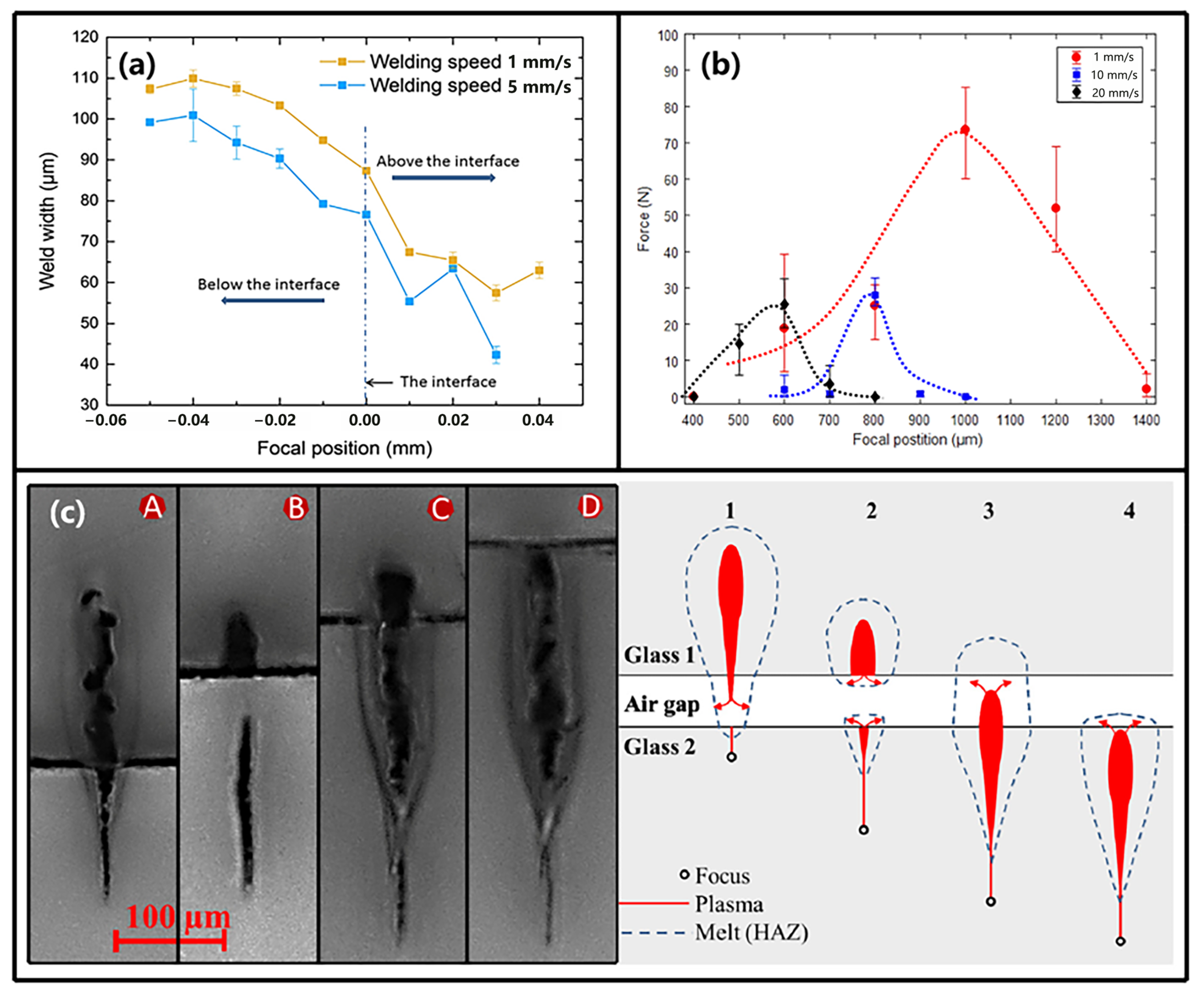
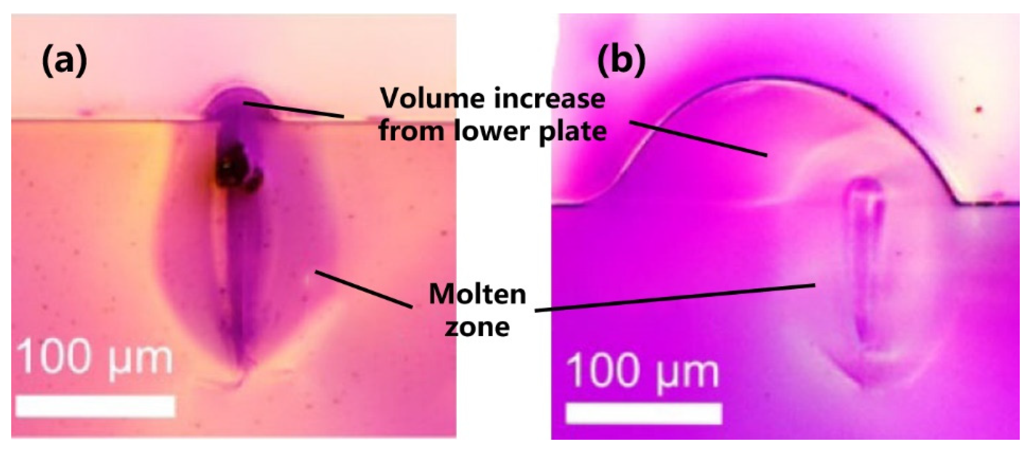
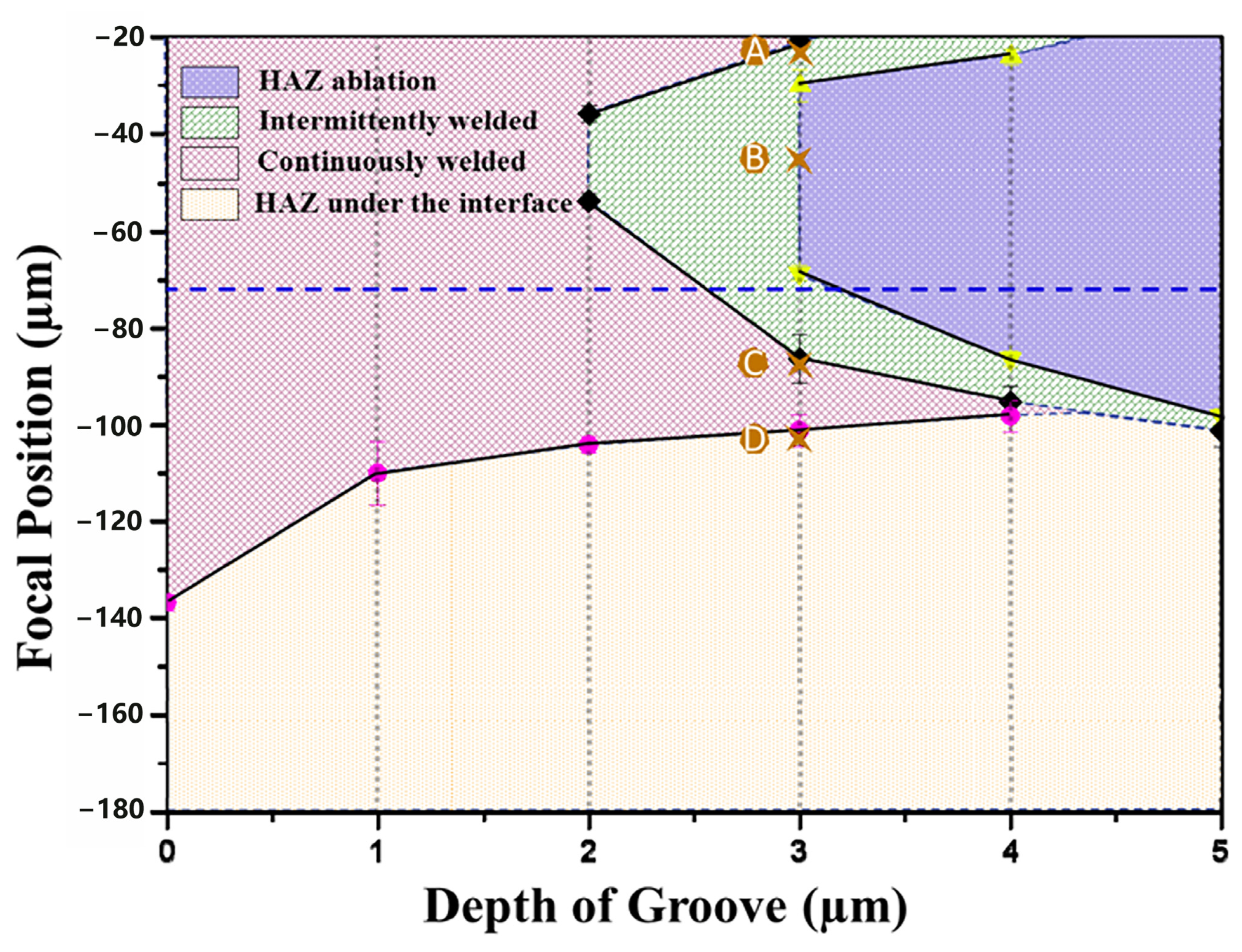
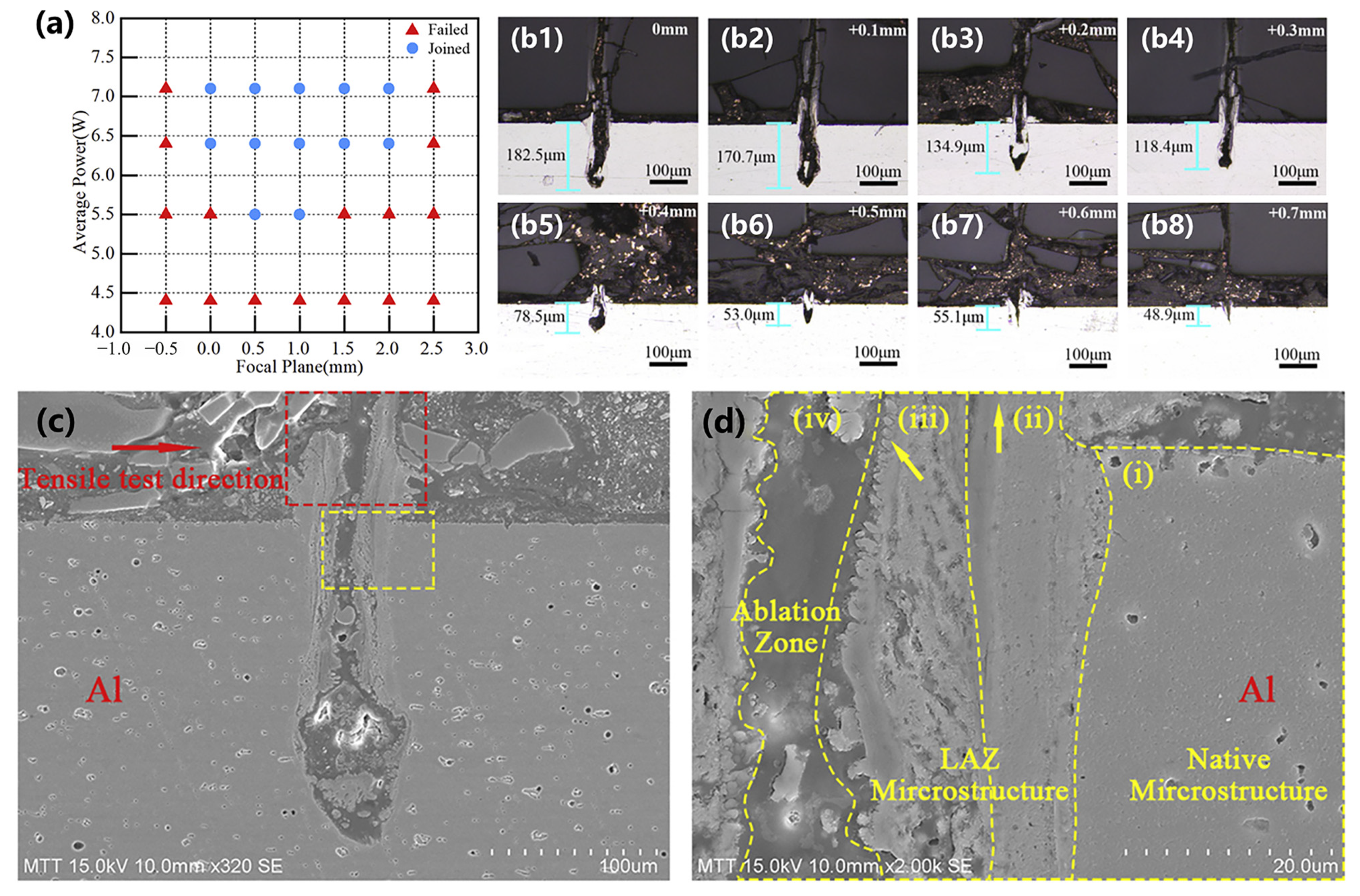
3.1.5. Focal Position
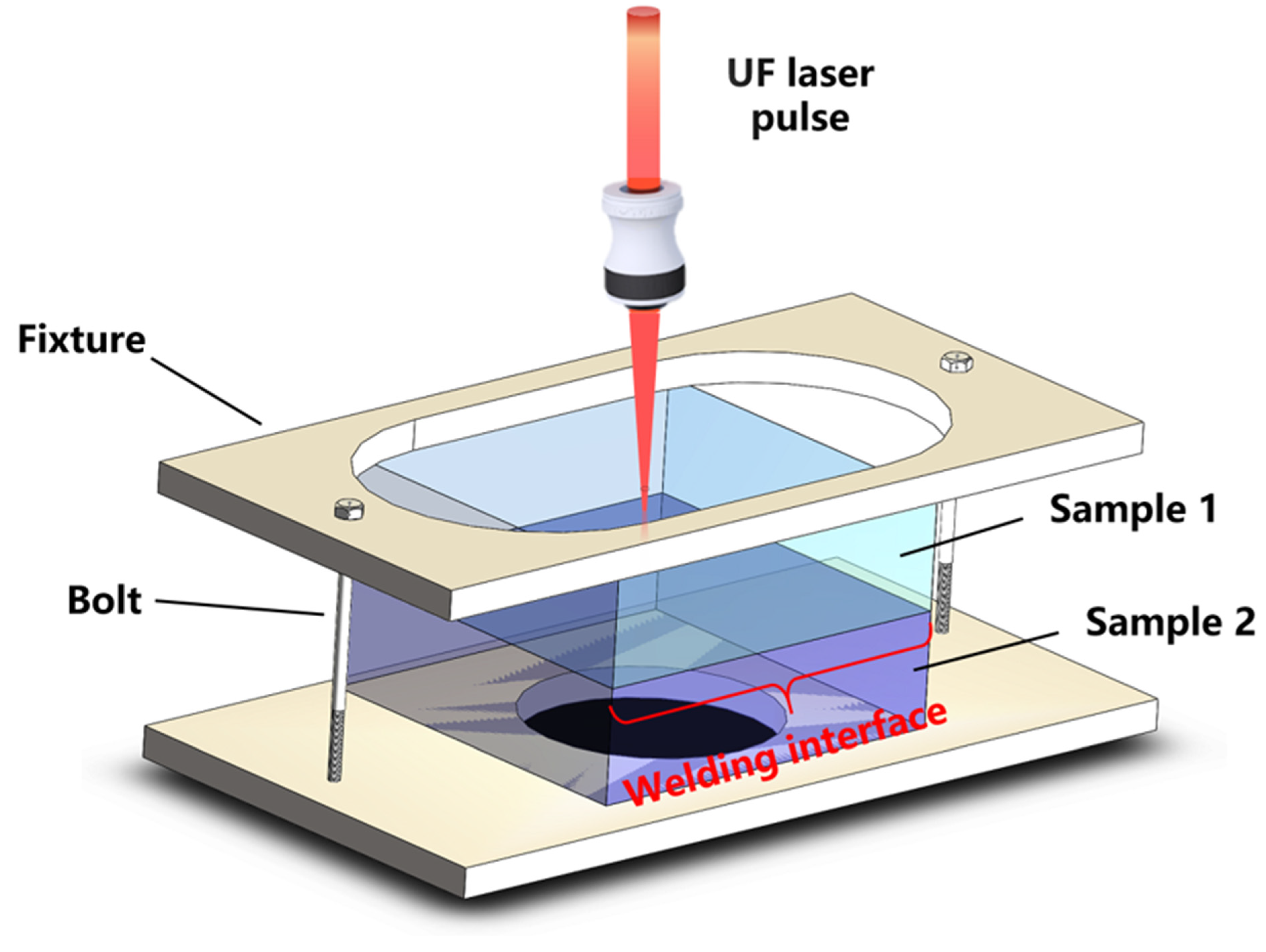
3.1.6. Contact States
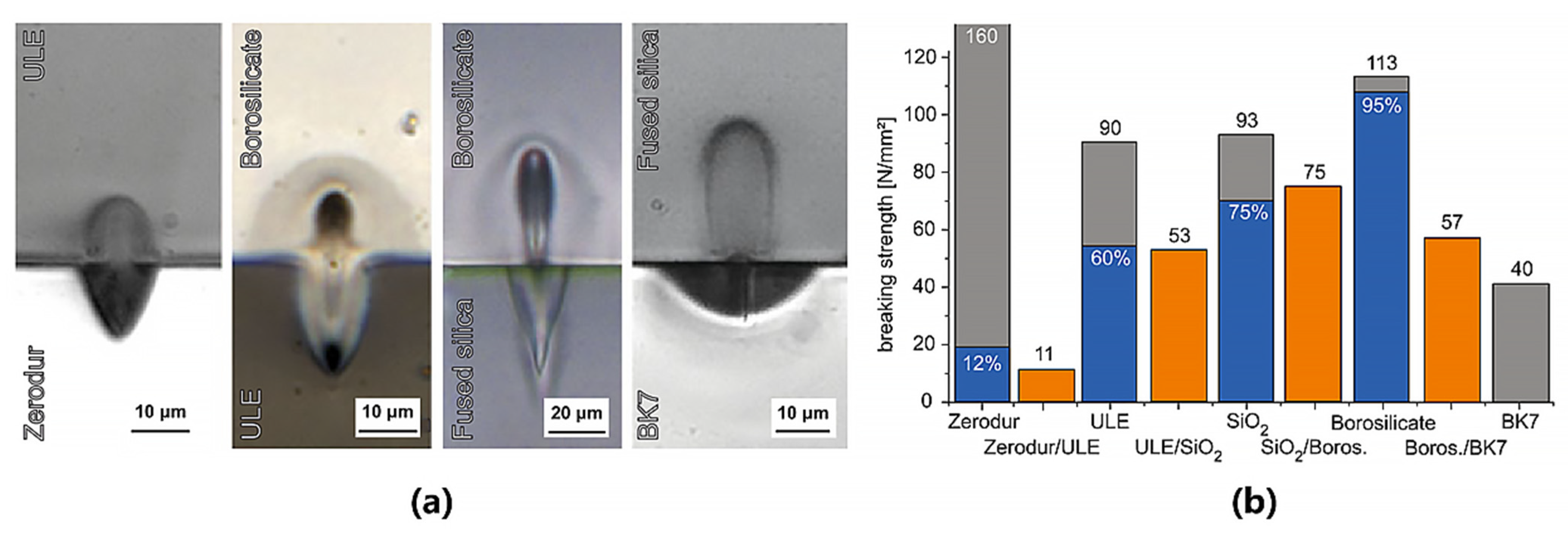
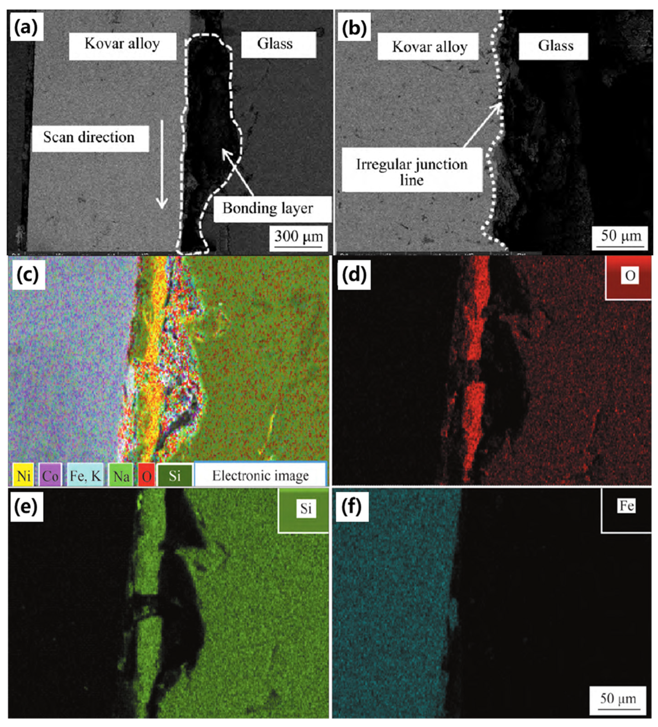
3.1.7. Dissimilar THB Material Combinations
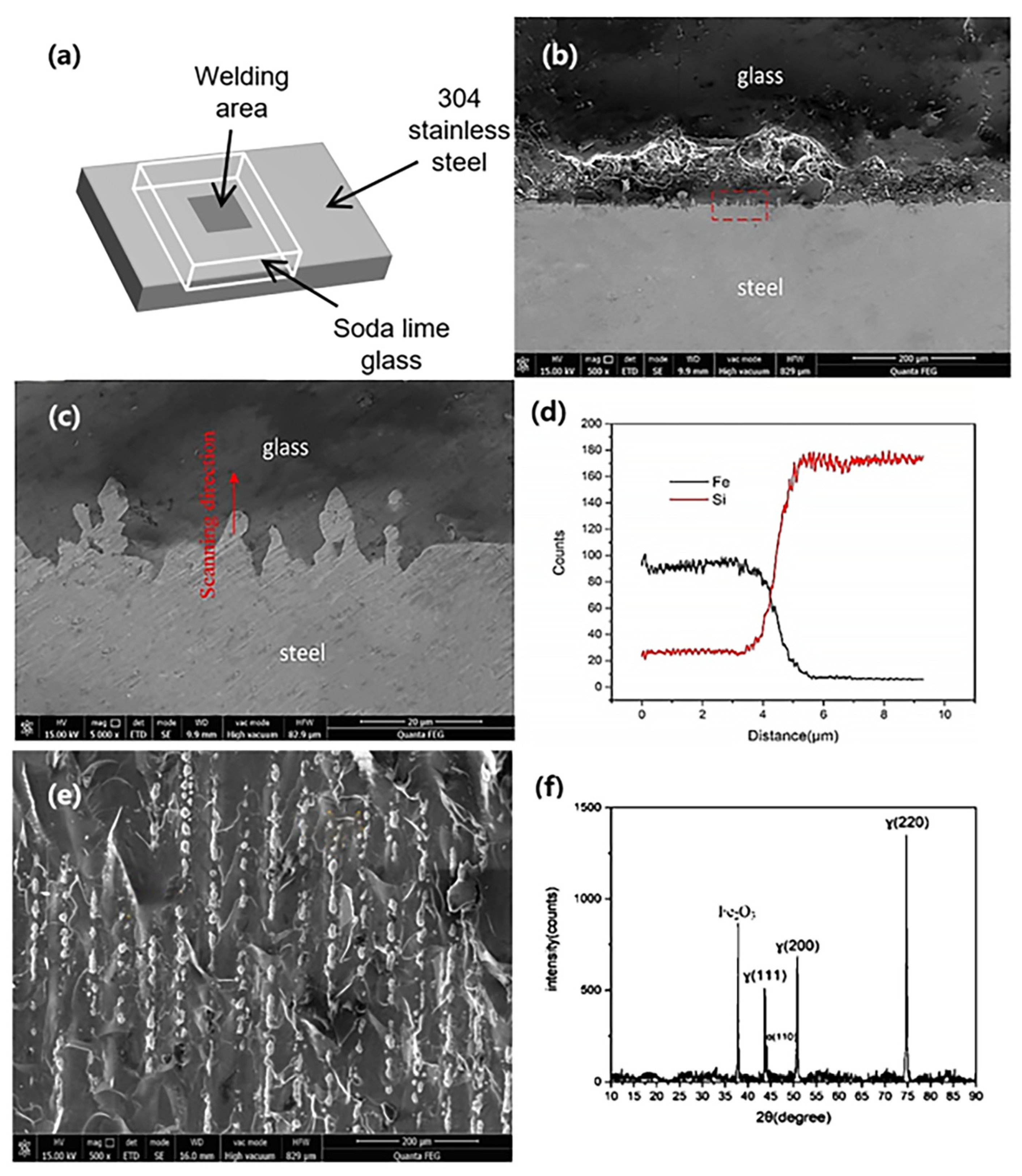
3.2. THB Material–Metal Microwelding
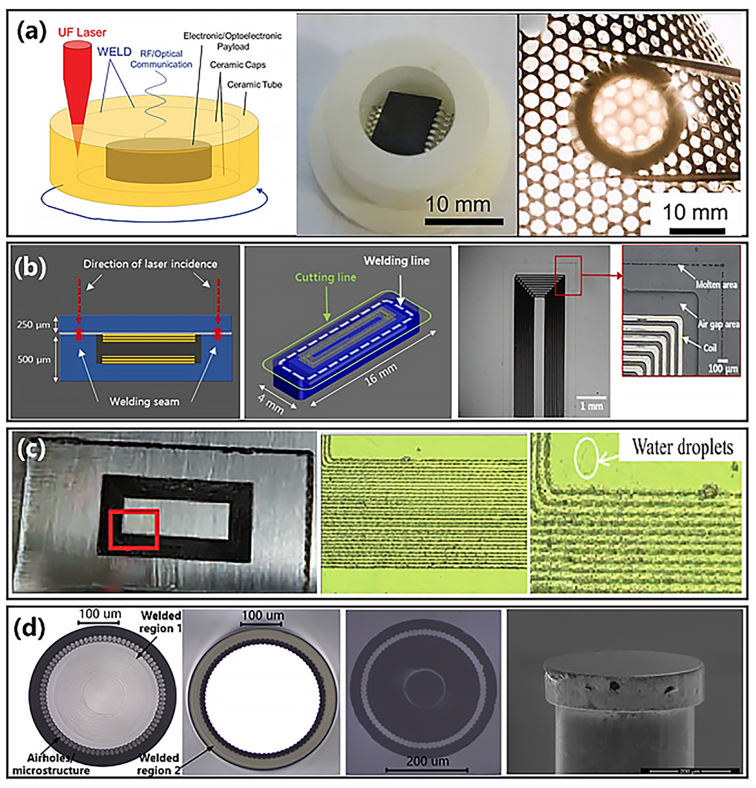
4. Application of Ultrafast Laser Microwelding of THB Materials and THB Material–Metals
5. Summary and Outlook
Author Contributions
Funding
Data Availability Statement
Acknowledgments
Conflicts of Interest
References
- Ji, C.H.; Huang, Y.J.; Chen, X.; Jiang, J.Y.; Guo, Z.J.; Long, Y. Direct microwelding of dissimilar glass and Kovar alloy without optical contact using femtosecond laser pulses. J. Cent. South Univ. 2022, 29, 3422–3435. [Google Scholar] [CrossRef]
- Cvecek, K.; Alexeev, I.; Miyamoto, I.; Schmidt, M. Defect formation in glass welding by means of ultra short laser pulses. In Proceedings of the 6th International Conference on Laser Assisted Net Shape Engineering, Erlangen, Germany, 21–24 September 2010; pp. 495–502. [Google Scholar]
- Helie, D.; Begin, M.; Lacroix, F.; Vallee, R. Reinforced direct bonding of optical materials by femtosecond laser welding. Appl. Opt. 2012, 51, 2098–2106. [Google Scholar] [CrossRef]
- Helie, D.; Lacroix, F.; Vallee, R. Bonding of Optical Materials by Femtosecond Laser Welding for Aerospace and High Power Laser Applications. In Proceedings of the Conference on Photonics North, Montreal, QC, Canada, 6–8 June 2012. [Google Scholar]
- Araceli de Pablos-Martin, A.; Grosse, C.; Cismak, A.; Hoche, T. Laser-Welded Steel Foils with Sapphire Substrates. Acta Metall. Sin. -Engl. Lett. 2016, 29, 683–688. [Google Scholar] [CrossRef]
- Lafon, R.E.; Li, S.X.; Micalizzi, F.; Lebair, S.W. Ultrafast laser bonding of glasses and crystals to metals for epoxy-free optical instruments. In Proceedings of the Conference on Components and Packaging for Laser Systems VI, San Francisco, CA, USA, 3–5 February 2020. [Google Scholar]
- Zhang, L.; Wu, H.; Wen, J.C.; Li, M.; Shao, X.Y.; Ma, X.Q. Glass to aluminum joining by forming a mechanical pin structure using femtosecond laser. J. Mater. Process. Technol. 2022, 302, 117504. [Google Scholar] [CrossRef]
- Overend, M.; Jin, Q.; Watson, J. The selection and performance of adhesives for a steel-glass connection. Int. J. Adhes. Adhes. 2011, 31, 587–597. [Google Scholar] [CrossRef]
- Knapkiewicz, P.; Cichy, B.; Posadowski, W.; Tadaszak, K.; Sniadek, P.; Dziuban, J. Anodic bonding of glass-to-glass through magnetron spattered nanometric silicon layer. In Proceedings of the 25th Eurosensors Conference, Athens, Greece, 4–7 September 2011. [Google Scholar]
- Wang, G.; Sun, X.N.; Xu, J.H.; Shan, Y.C.; Han, X.G.; Xu, J.J.; Li, J.T. Pressureless thermal diffusion bonding of transparent AlON ceramics by using a powder interlayer of parent material. Scr. Mater. 2019, 171, 118–121. [Google Scholar] [CrossRef]
- Li, C.; Zhang, K.P.; Mao, X.J.; Si, X.Q.; Lan, B.; Liu, Z.G.; Huang, Y.X.; Qi, J.L.; Feng, J.C.; Cao, J. Microstructure and mechanical properties of the AlON/Ti6Al4V active element brazing joint. Mater. Sci. Eng. A-Struct. Mater. Prop. Microstruct. Process. 2020, 793, 139859. [Google Scholar] [CrossRef]
- Xu, W.H.; Li, H.Y.; Yang, J.; Zhao, Y.X.; Oliveira, J.P.; Liu, H.B.; Zhang, Z.S.; Tan, C.W. Dynamic wetting and spreading mechanisms regulated by elemental Ni in a Mg/steel immiscible system during laser processing. J. Manuf. Process. 2022, 80, 600–611. [Google Scholar] [CrossRef]
- Zheng, M.; Zhang, H.; Gao, Y.F.; Zhao, Y.X.; Tan, C.W.; Song, X.G.; Yang, J. Influence of porous high entropy alloy coating on wetting behavior and interfacial microstructure of Al-Si alloy on steel substrate. J. Alloys Compd. 2022, 912, 165154. [Google Scholar] [CrossRef]
- Itoh, K.; Tamaki, T. Ultrafast laser microwelding for transparent and heterogeneous materials. In Proceedings of the Conference on Commercial and Biomedical Applications of Ultrafast Lasers VIII, San Jose, CA, USA, 20–23 January 2008. [Google Scholar]
- Carter, R.M.; Troughton, M.; Chen, J.Y.; Elder, I.; Thomson, R.R.; Lamb, R.A.; Esser, M.J.D.; Hand, D.P. Picosecond laser bonding of highly dissimilar materials. In Proceedings of the Conference on Emerging Imaging and Sensing Technologies, Edinburgh, Scotland, 28–29 September 2016. [Google Scholar]
- Carter, R.M.; Troughton, M.; Chen, J.; Elder, I.; Thomson, R.R.; Daniel Esser, M.J.; Lamb, R.A.; Hand, D.P. Towards industrial ultrafast laser microwelding: SiO2 and BK7 to aluminum alloy. Appl. Opt. 2017, 56, 4873–4881. [Google Scholar] [CrossRef]
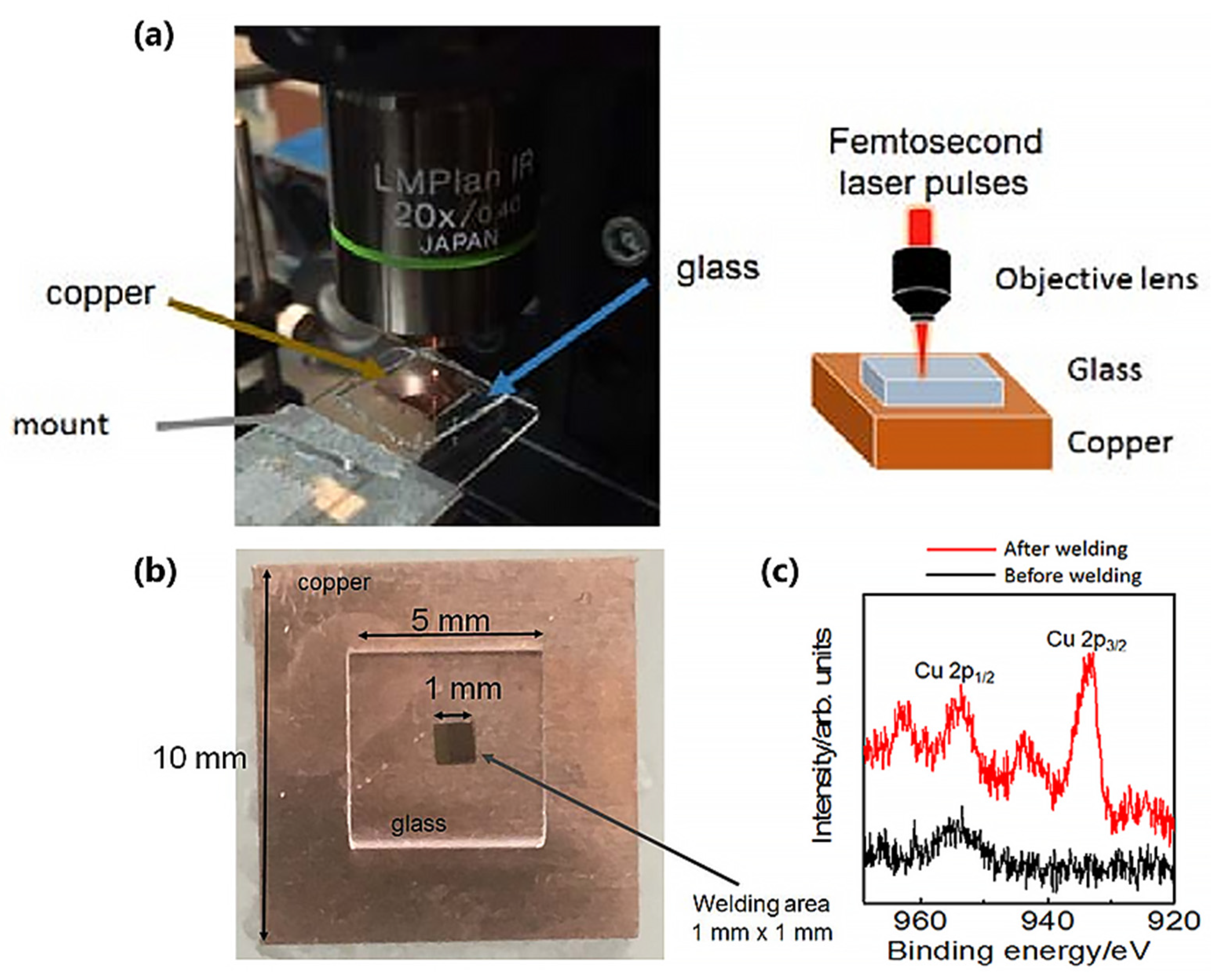
- Ozeki, Y.; Inoue, T.; Tamaki, T.; Yamaguchi, H.; Onda, S.; Watanabe, W.; Sano, T.; Nishiuchi, S.; Hirose, A.; Itoh, K. Direct Welding between Copper and Glass Substrates with Femtosecond Laser Pulses. Appl. Phys. Express 2008, 1, 082601. [Google Scholar] [CrossRef]
- Carter, R.M.; Chen, J.Y.; Shephard, J.D.; Thomson, R.R.; Hand, D.P. Picosecond laser welding of similar and dissimilar materials. Appl. Opt. 2014, 53, 4233–4238. [Google Scholar] [CrossRef] [PubMed]
- Watanabe, W.; Onda, S.; Tamaki, T.; Itoh, K.; Nishii, J. Space-selective laser joining of dissimilar transparent materials using femtosecond laser pulses. Appl. Phys. Lett. 2006, 89, 021106. [Google Scholar] [CrossRef]
- Richter, S.; Nolte, S.; Tunnermann, A. Ultrashort pulse laser welding—A new approach for high-stability bonding of different glasses. In Proceedings of the 7th Conference on Laser Assisted Net shape Engineering (LANE)/International Conference on Photonic Technologies, Furth, Germany, 12–15 November 2012; pp. 556–562. [Google Scholar]
- Tan, H.; Duan, J. One-step femtosecond laser welding and internal machining of three glass substrates. Appl. Phys. A-Mater. Sci. Process. 2017, 123, 377. [Google Scholar] [CrossRef]
- Kim, S.; Park, J.; So, S.; Ahn, S.; Choi, J.; Koo, C.; Joung, Y.H. Characteristics of an Implantable Blood Pressure Sensor Packaged by Ultrafast Laser Microwelding. Sensors 2019, 19, 1801. [Google Scholar] [CrossRef]
- Lipateva, T.O.; Okhrimchuk, A.G.; Lipatiev, A.S.; Karateev, I.A.; Fedotov, S.S.; Lotarev, S.V.; Shestakov, A.V.; Sigaev, V.N. Robust and adhesive-free joint of Nd:YAG crystals by femtosecond laser-assisted welding. Opt. Laser Technol. 2022, 146, 107594. [Google Scholar] [CrossRef]
- Tamaki, T.; Watanabe, W.; Nishii, J.; Itoh, K. Welding of Transparent Materials Using Femtosecond Laser Pulses. Jpn. J. Appl. Phys. 2005, 44, L687. [Google Scholar] [CrossRef]
- Miyamoto, I.; Cvecek, K.; Okamoto, Y.; Schmidt, M. Internal modification of glass by ultrashort laser pulse and its application to microwelding. Appl. Phys. A-Mater. Sci. Process. 2014, 114, 187–208. [Google Scholar] [CrossRef]
- Eaton, S.M.; Cerullo, G.; Osellame, R. Fundamentals of Femtosecond Laser Modification of Bulk Dielectrics. In Femtosecond Laser Micromaching: Photonic and Microfluidic Devices in Transparent Materials; Osellame, R., Cerullo, G., Ramponi, R., Eds.; Springer: Berlin, Germany, 2012; Volume 123, pp. 3–18. [Google Scholar]
- Matsuyoshi, S.; Mizuguchi, Y.; Muratsugu, A.; Yamada, H.; Tamaki, T.; Watanabe, W. Welding of Glass and Copper with a Rough Surface using Femtosecond Fiber Laser Pulses. J. Laser Micro Nanoeng. 2018, 13, 21–25. [Google Scholar] [CrossRef]
- Sundaram, S.K.; Mazur, E. Inducing and probing non-thermal transitions in semiconductors using femtosecond laser pulses. Nat. Mater. 2002, 1, 217–224. [Google Scholar] [CrossRef]
- Rethfeld, B.; Sokolowski-Tinten, K.; von der Linde, D.; Anisimov, S.I. Timescales in the response of materials to femtosecond laser excitation. Appl. Phys. A 2004, 79, 767–769. [Google Scholar] [CrossRef]
- Phillips, K.C.; Gandhi, H.H.; Mazur, E.; Sundaram, S.K. Ultrafast laser processing of materials: A review. Adv. Opt. Photonics 2015, 7, 684–712. [Google Scholar] [CrossRef]
- Chen, Z.J.; Yang, J.; Liu, H.B.; Zhao, Y.X.; Pan, R. A short review on functionalized metallic surfaces by ultrafast laser micromachining. Int. J. Adv. Manuf. Technol. 2022, 119, 6919–6948. [Google Scholar] [CrossRef]
- Tan, D.Z.; Sharafudeen, K.N.; Yue, Y.Z.; Qiu, J.R. Femtosecond laser induced phenomena in transparent solid materials: Fundamentals and applications. Prog. Mater. Sci. 2016, 76, 154–228. [Google Scholar] [CrossRef]
- Bulgakova, N.M.; Stoian, R.; Rosenfeld, A.; Hertel, I.V.; Campbell, E.E.B. Electronic transport and consequences for material removal in ultrafast pulsed laser ablation of materials. Phys. Rev. B 2004, 69, 054102. [Google Scholar] [CrossRef]
- Cvecek, K.; Odato, R.; Dehmel, S.; Miyamoto, I.; Schmidt, M. Gap bridging in joining of glass using ultra short laser pulses. Opt. Express 2015, 23, 5681–5693. [Google Scholar] [CrossRef]
- Wang, Y.P.; Li, Y.; Ao, S.S.; Luo, Z.; Zhang, D. Welding of 304 stainless steel and glass using high-repetition-frequency femtosecond laser. Mater. Res. Express 2021, 8, 106523. [Google Scholar] [CrossRef]
- Zhang, G.D.; Cheng, G.H. Direct welding of glass and metal by 1 kHz femtosecond laser pulses. Appl. Opt. 2015, 54, 8957–8961. [Google Scholar] [CrossRef]
- Ciuca, O.P.; Carter, R.M.; Prangnell, P.B.; Hand, D.P. Characterisation of weld zone reactions in dissimilar glass-to-aluminium pulsed picosecond laser welds. Mater. Charact. 2016, 120, 53–62. [Google Scholar] [CrossRef]
- Miyamoto, I.; Horn, A.; Gottmann, J.; Wortmann, D.; Yoshino, F. Fusion welding of glass using femtosecond laser pulses with high-repetition rates. J. Laser Micro/Nanoeng. 2007, 2, 57–63. [Google Scholar] [CrossRef]
- Huang, S.; Chen, R.; Zhang, H.; Ye, J.; Yang, X.; Sheng, J. A study of welding process in connecting borosilicate glass by picosecond laser pulses based on response surface methodology. Opt. Laser Technol. 2020, 131, 106427. [Google Scholar] [CrossRef]
- Tamaki, T.; Watanabe, W.; Itoh, K. Laser micro-welding of transparent materials by a localized heat accumulation effect using a femtosecond fiber laser at 1558 nm. Opt. Express 2006, 14, 10460–10468. [Google Scholar] [CrossRef]
- Chen, H.; Rong, Y.; Huang, Y.; Wu, C. Crack suppression of glass welding by ultrafast laser without optical contact based on light modulation. Opt. Laser Technol. 2023, 164, 109466. [Google Scholar] [CrossRef]
- Cheng, J.; Liu, C.-S.; Shang, S.; Liu, D.; Perrie, W.; Dearden, G.; Watkins, K. A review of ultrafast laser materials micromachining. Opt. Laser Technol. 2013, 46, 88–102. [Google Scholar] [CrossRef]
- Chen, J.; Carter, R.M.; Thomson, R.R.; Hand, D.P. Avoiding the requirement for pre-existing optical contact during picosecond laser glass-to-glass welding. Opt. Express 2015, 23, 18645–18657. [Google Scholar] [CrossRef]
- Boyd, R.W. Chapter 7—Spontaneous Light Scattering and Acousto-optics. In Nonlinear Optics; Boyd, R.W., Ed.; Academic Press: San Diego, CA, USA, 1992; pp. 287–324. [Google Scholar] [CrossRef]
- Sudrie, L.; Couairon, A.; Franco, M.; Lamouroux, B.; Prade, B.; Tzortzakis, S.; Mysyrowicz, A. Femtosecond laser-induced damage and filamentary propagation in fused silica. Phys. Rev. Lett. 2002, 89, 186601. [Google Scholar] [CrossRef] [PubMed]
- Eaton, S.M.; Zhang, H.; Herman, P.R.; Yoshino, F.; Shah, L.; Bovatsek, J.; Arai, A.Y. Heat accumulation effects in femtosecond laser-written waveguides with variable repetition rate. Opt. Express 2005, 13, 4708–4716. [Google Scholar] [CrossRef]
- Sugioka, K.; Iida, M.; Takai, H.; Micorikawa, K. Efficient microwelding of glass substrates by ultrafast laser irradiation using a double-pulse train. Opt. Lett. 2011, 36, 2734–2736. [Google Scholar] [CrossRef] [PubMed]
- Wu, S.Z.; Wu, D.; Xu, J.; Wang, H.Y.; Makimura, T.; Sugioka, K.; Midorikawa, K. Absorption mechanism of the second pulse in double-pulse femtosecond laser glass microwelding. Opt. Express 2013, 21, 24049–24059. [Google Scholar] [CrossRef]
- Stuart, B.; Feit, M.; Herman, S.; Rubenchik, A.; Shore, B.; Perry, M. Nanosecond-to-femtosecond laser-induced breakdown in dielectrics. Phys. Rev. B Condens. Matter 1996, 53, 1749–1761. [Google Scholar] [CrossRef] [PubMed]
- Penilla, E.H.; Devia-Cruz, L.F.; Wieg, A.T.; Martinez-Torres, P.; Cuando-Espitia, N.; Sellappan, P.; Kodera, Y.; Aguilar, G.; Garay, J.E. Ultrafast laser welding of ceramics. Science 2019, 365, 803–808. [Google Scholar] [CrossRef]
- Nolte, S.; Momma, C.; Jacobs, H.; Tünnermann, A.; Chichkov, B.N.; Wellegehausen, B.; Welling, H. Ablation of metals by ultrashort laser pulses. J. Opt. Soc. Am. B 1997, 14, 2716–2722. [Google Scholar] [CrossRef]
- Fedosejevs, R.; Ottmann, R.; Sigel, R.; Kühnle, G.; Szatmari, S.; Schäfer, F.P. Absorption of femtosecond laser pulses in high-density plasma. Phys. Rev. Lett. 1990, 64, 1250–1253. [Google Scholar] [CrossRef] [PubMed]
- Kongsuwan, P.; Satoh, G.; Yao, Y.L. Transmission Welding of Glass by Femtosecond Laser: Mechanism and Fracture Strength. J. Manuf. Sci. Eng.-Trans. Asme 2012, 134, 011004. [Google Scholar] [CrossRef]
- Miao, Y.; Ting, H.; Rongshi, X. Long Focal Length Green Femtosecond Laser Welding of Glass. Chin. J. Lasers 2020, 47, 0902005. [Google Scholar] [CrossRef]
- Zhao, K.; Wang, H.; Yan, J.; Shen, H. Welding Fused Silica Glass by Picosecond Pulsed Laser With Low Numerical Aperture. J. Micro Nano-Manuf. 2019, 7, 041007. [Google Scholar] [CrossRef]
- Richter, S.; Zimmermann, F.; Tunnermann, A.; Nolte, S. Laser welding of glasses at high repetition rates—Fundamentals and prospects. Opt. Laser Technol. 2016, 83, 59–66. [Google Scholar] [CrossRef]
- Zhang, J.J.; Xu, S.Z.; Dong, Y.K.; Zhang, C.Z.; Li, J.M.; Guo, L.; Zhang, Q.M. Microwelding of glass to silicon by green ultrafast laser pulses. Opt. Laser Technol. 2019, 120, 105720. [Google Scholar] [CrossRef]
- Zhang, J.J.; Chen, S.H.; Lu, H.L.; Huang, M.H.; Li, J.M.; Guo, L.; Lue, Q.T.; Zhang, Q.M. The effect of gap on the quality of glass-to-glass welding using a picosecond laser. Opt. Lasers Eng. 2020, 134, 106248. [Google Scholar] [CrossRef]
- Lipat’eva, T.O.; Fedotov, S.S.; Lipat’ev, A.S.; Lotarev, S.V.; Shakhgil’dyan, G.Y.; Ryabov, K.V.; Sigaev, V.N. Precision Laser Welding of Silica Glass with Iron-Nickel Alloy. Glass Ceram. 2021, 77, 435–437. [Google Scholar] [CrossRef]
- Lacroix, F.; Helie, D.; Vallee, R. Optical Bonding Reinforced by Femtosecond Laser Welding. In Proceedings of the Conference on Optical Manufacturing and Testing IX, San Diego, CA, USA, 22–24 August 2011. [Google Scholar]
- Chen, H.; Deng, L.M.; Duan, J.; Zeng, X.Y. Picosecond laser welding of glasses with a large gap by a rapid oscillating scan. Opt. Lett. 2019, 44, 2570–2573. [Google Scholar] [CrossRef]
- Watanabe, W.; Tamaki, T.; Itoh, K. Filamentation in laser microprocessing and microwelding. In Proceedings of the International Conference on Lasers, Applications, and Technologies, Minsk, Byelarus, 28 May–1 June 2007. [Google Scholar]
- Jia, X.; Li, K.; Li, Z.; Wang, C.; Chen, J.; Cui, S. Multi-scan picosecond laser welding of non-optical contact soda lime glass. Opt. Laser Technol. 2023, 161, 109164. [Google Scholar] [CrossRef]
- Richter, S.; Zimmermann, F.; Doring, S.; Tunnermann, A.; Nolte, S. Ultrashort high repetition rate exposure of dielectric materials: Laser bonding of glasses analyzed by micro-Raman spectroscopy. Appl. Phys. A-Mater. Sci. Process. 2013, 110, 9–15. [Google Scholar] [CrossRef]
- Liu, Z.; Yang, J.; Li, Y.; Li, W.; Chen, J.; Shen, L.; Zhang, P.; Zhishui, Y. Wetting and Spreading Behaviors of Al-Si Alloy on Surface Textured Stainless Steel by Ultrafast Laser. Appl. Surf. Sci. 2020, 520, 146316. [Google Scholar] [CrossRef]
- Li, H.; Li, L.Q.; Huang, R.; Tan, C.; Yang, J.; Hongbo, X.; Chen, B. The effect of surface texturing on the laser-induced wetting behavior of AlSi5 alloy on Ti6Al4V alloy. Appl. Surf. Sci. 2021, 566, 150630. [Google Scholar] [CrossRef]
- Quintino, L.; Liu, L.; Miranda, R.M.; Silva, R.J.C.; Hu, A.; Zhou, Y. Bonding NiTi to glass with femtosecond laser pulses. Mater. Lett. 2013, 98, 142–145. [Google Scholar] [CrossRef]
- Mingareev, I.; Bautista, N.; Yadav, D.; Bhanderi, A. Ultrafast laser deposition of powder materials on glass. Opt. Laser Technol. 2023, 160, 109078. [Google Scholar] [CrossRef]
- Pan, R.; Yang, D.; Zhou, T.; Feng, Y.; Dong, Z.; Yan, Z.; Li, P.; Yang, J.; Chen, S. Micro-welding of sapphire and metal by femtosecond laser. Ceram. Int. 2023; in press. [Google Scholar] [CrossRef]
- Labutin, T.A.; Lednev, V.N.; Ilyin, A.A.; Popov, A.M. Femtosecond laser-induced breakdown spectroscopy. J. Anal. At. Spectrom. 2016, 31, 90–118. [Google Scholar] [CrossRef]
- Watanabe, W.; Li, Y.; Itoh, K. Ultrafast laser micro-processing of transparent material. Opt. Laser Technol. 2016, 78, 52–61. [Google Scholar] [CrossRef]
- Tong, T.; Li, J.; Longtin, J.P. Real-time control of ultrafast laser micromachining by laser-induced breakdown spectroscopy. Appl. Opt. 2004, 43, 1971–1980. [Google Scholar] [CrossRef]
- Hou, H.; Cheng, L.; Richardson, T.; Chen, G.; Doeff, M.; Zheng, R.; Russo, R.; Zorba, V. Three-dimensional elemental imaging of Li-ion solid-state electrolytes using fs-laser induced breakdown spectroscopy (LIBS). J. Anal. At. Spectrom. 2015, 30, 2295–2302. [Google Scholar] [CrossRef]
- Wessel, W.; Brueckner-Foit, A.; Mildner, J.; Englert, L.; Haag, L.; Horn, A.; Wollenhaupt, M.; Baumert, T. Use of femtosecond laser-induced breakdown spectroscopy (fs-LIBS) for micro-crack analysis on the surface. Eng. Fract. Mech. 2010, 77, 1874–1883. [Google Scholar] [CrossRef]
- Yoshino, T.; Ozeki, Y.; Matsumoto, M.; Itoh, K. In situ Micro-Raman Investigation of Spatio-Temporal Evolution of Heat in Ultrafast Laser Microprocessing of Glass. Jpn. J. Appl. Phys. 2012, 51, 102403. [Google Scholar] [CrossRef]
- Jonusauskas, L.; Rekstyte, S.; Buividas, R.; Butkus, S.; Gadonas, R.; Juodkazis, S.; Malinauskas, M. Hybrid subtractive-additive-welding microfabrication for lab-on-chip applications via single amplified femtosecond laser source. Opt. Eng. 2017, 56, 094108. [Google Scholar] [CrossRef]
- Fujiwara, J.; Tamaki, T. Measuring sealing degree of welded glass substrates after ultrafast laser microwelding. Appl. Phys. A 2022, 128, 1076. [Google Scholar] [CrossRef]
- Helie, D.; Gouin, S.; Vallee, R. Assembling an endcap to optical fibers by femtosecond laser welding and milling. Opt. Mater. Express 2013, 3, 1742–1754. [Google Scholar] [CrossRef]
- Tan, H.; Yang, W.; Huang, Q.; Pan, J.; Li, C.; Fu, X. Embedded thin film fabrication via glass welding by an ultrafast laser. J. Asian Ceram. Soc. 2023, 11, 62–67. [Google Scholar] [CrossRef]
- Miyamoto, I.; Cvecek, K.; Schmidt, M. Advances of Laser Welding Technology of Glass -Science and Technology. J. Laser Micro Nanoeng. 2020, 15, 63–76. [Google Scholar] [CrossRef]
- Wen, J.; Zhang, L.; Wu, H.; Li, M.; Ma, X. Molecular Dynamics Simulation of Aluminum-Fused Silica Interface Shot by Femtosecond Laser. Laser Optoelectron. Prog. 2023, 60, 0114011. [Google Scholar] [CrossRef]
- Zhang, S.W.; Kong, M.; Miao, H.; Memon, S.; Zhang, Y.J.; Liu, S.X. Transient temperature and stress fields on bonding small glass pieces to solder glass by laser welding: Numerical modelling and experimental validation. Sol. Energy 2020, 209, 350–362. [Google Scholar] [CrossRef]
- Xue, J.; Guo, W.; Yang, J.; Xia, M.; Zhao, G.; Tan, C.; Wan, Z.; Chi, J.; Zhang, H. In-situ observation of microcrack initiation and damage nucleation modes on the HAZ of laser-welded DP1180 joint. J. Mater. Sci. Technol. 2023, 148, 138–149. [Google Scholar] [CrossRef]


| Welded Materials | Laser | Remarks | Ref. | ||
|---|---|---|---|---|---|
| Pulse Width | Wave-Length | Rep. Rate | |||
| Cu/non-alkali glass | 130 fs | 800 nm | 1 kHz | 1. optical polishing treatment and mechanical pressing; 2. successful joining without voids or cracks; 3. joint strength by fs laser: >16 MPa; | [17] |
| 600 ns | 527 nm | 1 kHz | |||
| Cu/borosilicate | 130 fs | 800 nm | 1 kHz | 1. polishing treatment and pressure assistance; 2. joint strength: 20 MPa; | [14] |
| Cu/fused silica W/fused silica | 70 fs | 790 nm | 250 kHz | 1. polishing treatment and clamping assistance; 2. Cu/fused silica joint strength: 9 MPa; | [60] |
| NiTi/glass | 35 fs | 800 nm | 1 kHz | 1. bonding micrometric NiTi particle to glass; 2. free of cracks; | [67] |
| Al/SiO2 Cu/SiO2 SS/borosilicate SS/Sapphire | 10 ps | 1030 nm | 400 kHz | 1. polishing treatment and clamping assistance; 2. dissimilar material welding of glass and sapphire to aluminum and stainless steel has been demonstrated for the first time; 3. in all cases the welds fractured around the modified region within the glass; | [18] |
| Cu/Alumina-silicate Al/Alumina-silicate Steel/Alumina-silicate | 160 fs | 800 nm | 1 kHz | 1. polishing treatment and no pressure assistance; 2. Cu/glass joint shear strength: 2.34 MPa; 3. micron/nanometer-sized metal particles produced by laser ablation as adhesive; | [36] |
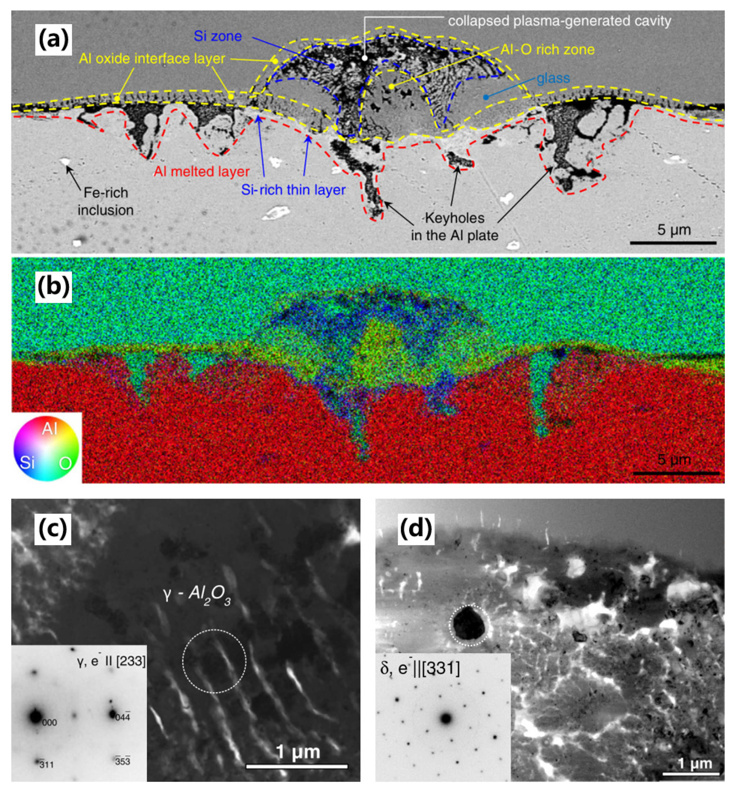
| Al/fused silica glass | 5.9 ps | 1030 nm | 400 kHz | 1. polishing treatment and clamping assistance; 2. joint formation process: nonlinear absorption, creation of plasma cavity and secondary keyholes; 3. extensive reaction was observed in the weld zone; 4. formation of nanocrystalline Si and, transitional alumina phases γ- and δ-Al2 O3: the first time such transitional alumina phases have been reported in a laser weld; | [37] |
| AlSi/Nd: YAG | 5.9 ps | 1030 nm | 400 kHz | 1. polishing treatment and pressure assistance; 2. bonding of two materials with close thermal properties; | [15] |
| Al 6082/SiO2 Al 6082/BK7 | 5.9 ps | 1030 nm | 400 kHz | 1. pressure assistance and no optically polishing treatment; 2. a double-pass welding process applied; 3. parameter mapping: focal plane and incident power; 4. optimized Al 6082/BK7 bonding strength: 13 MPa; | [16] |
| Cu/glass | 550 fs | 1064 nm | 1 MHz | 1. no polishing treatment on metal and no pressure assistance; 2. parameter mapping: scanning speed, line interval and focal position; 3. joint shear strength: 1 MPa; | [27] |
| 304L SS/CaF2 | 150 fs | 780 nm | 1 kHz | 1. polishing treatment and pressure assistance; 2. the ablation debris solidifies and creates a bridging bond between the glass and metal surfaces; 3. significant material mixing at the interface responsible for the bond; 4. no visible gap between the CaF2 and stainless steel; 5. other material combinations welded but not rigorously tested: fused silica–copper, Zerodur–Invar, fused silica–fused silica, fused silica–Zerodur, sapphire–titanium, fused silica–aluminum, sapphire–molybdenum, sapphire–Invar and diamond–Invar; | [6] |
| 304 SS/soda lime glass | 270 fs | 1040 nm | 400 kHz | 1. surface grinding treatment but non-optical contact condition; 2. no element penetration at the junction; 3. joining mechanism: mechanical mixing, wetting and adsorption; 4. parameter mapping: pulse energy, focal position, repetition frequency and welding speed; 5. optimized joint strength: 8.79 MPa; | [35] |
| Al 6082/SiO2 | 35 fs | 800 nm | 1 kHz | 1. pressure assistance and no polishing treatment; 2. forming a mechanical pin structure consisting of adhesive regions and a concave-convex structure between two substrates; 3. shear strength: >100 MPa; | [7] |
| Kover/soda lime glass | 300 fs | 1030 nm | 1 kHz | 1. no polishing treatment and no pressure assistance; 2. micron/nanometer-sized metal particles condensed by plasma sprays as an adhesive part in the welding process; 3. material mixing and interdiffusion occurred; 4. shear strength: 2 MPa; 5. other material combinations welded: Cu-soda lime glass, Al6063-soda lime glass and sapphire-ceramic; | [1] |
| Tin powder/borosilicate glass Nickel powder/borosilicate glass Copper powder/borosilicate glass 304 stainless steel powder/borosilicate glass | 350 fs | 1030 nm | 1.5 MHz | 1. successfully and reproducibly deposited continuous tracks of powder materials on glass; 2. a relatively thin layer of approx. 3–4 µm occurring at the interface between the glass and the deposited powder; 3. an inhomogeneous material composition of the interface region 4. laser-deposited layers reaching thickness up to 60–70 μm depending on the process conditions. | [68] |
| Invar 36 alloy/sapphire | 800 fs | 1030 nm | 200 kHz | 1. polishing treatment and pressure assistance; 2. successful joining without any void and microcracks; 3. welding interface consisting of a <1 μm mixed phase region with Fe-36Ni particles and sapphire; 4. bonding mechanism: chemical bonding and mechanical interlocking; 5. optimized shear strength: 108.35 MPa; | [69] |
Disclaimer/Publisher’s Note: The statements, opinions and data contained in all publications are solely those of the individual author(s) and contributor(s) and not of MDPI and/or the editor(s). MDPI and/or the editor(s) disclaim responsibility for any injury to people or property resulting from any ideas, methods, instructions or products referred to in the content. |
© 2023 by the authors. Licensee MDPI, Basel, Switzerland. This article is an open access article distributed under the terms and conditions of the Creative Commons Attribution (CC BY) license (https://creativecommons.org/licenses/by/4.0/).
Share and Cite
Xu, J.; Jiang, Q.; Yang, J.; Cui, J.; Zhao, Y.; Zheng, M.; Oliveira, J.P.; Zeng, Z.; Pan, R.; Chen, S. A Review on Ultrafast Laser Microwelding of Transparent Materials and Transparent Material–Metals. Metals 2023, 13, 876. https://doi.org/10.3390/met13050876
Xu J, Jiang Q, Yang J, Cui J, Zhao Y, Zheng M, Oliveira JP, Zeng Z, Pan R, Chen S. A Review on Ultrafast Laser Microwelding of Transparent Materials and Transparent Material–Metals. Metals. 2023; 13(5):876. https://doi.org/10.3390/met13050876
Chicago/Turabian StyleXu, Jiayi, Qing Jiang, Jin Yang, Jiangmei Cui, Yixuan Zhao, Min Zheng, J. P. Oliveira, Zhi Zeng, Rui Pan, and Shujun Chen. 2023. "A Review on Ultrafast Laser Microwelding of Transparent Materials and Transparent Material–Metals" Metals 13, no. 5: 876. https://doi.org/10.3390/met13050876