Article

Microstructure Evolution and Mechanical Properties of TiC Coating over Inconel 625 Obtained by Vacuum Electron Beam Surface Alloying

1
Engineering Research Center of Ministry of Education of Heavy Machinery, Taiyuan University of Science and Technology, Taiyuan 030024, China
2
Shanxi Provincial Key Laboratory of Metallurgical Device Design Theory and Technology, Taiyuan 030024, China
*
Author to whom correspondence should be addressed.
Metals 2023, 13(2), 275; https://doi.org/10.3390/met13020275
Submission received: 19 December 2022 / Revised: 26 January 2023 / Accepted: 27 January 2023 / Published: 30 January 2023
(This article belongs to the Special Issue Advances in Metallic Materials for Projectile Manufacturing)

Abstract

:
Inconel 625 nickel-base alloy was modified by electron beam surface alloying (EBSA) with TiC as the coating at different scanning speeds (80 mm/min, 100 mm/min, and 120 mm/min). Its microstructure evolution and friction and wear evolution were characterized using electron backscatter diffraction (EBSD), a microhardness tester, and a friction and wear tester (RTEC). The results indicated that the FCC phase in the microstructure of the Inconel 625 nickel-base alloy is island-shaped after EBSA. At different scanning speeds, the austenitic texture types will eventually form primarily S-texture accompanied by Goss texture and Brass texture of varying strengths. With an increase in scanning speed, the surface hardness of nickel-base alloys decreases. The highest surface hardness was 457 HB at 80 mm/min, and the surface hardness was 1.936 times higher than that of the base material. With an increase in scanning speed, the wear resistance of the nickel-base alloy plates decreased gradually. At the scanning speed of 80 mm/min, the wear volume and wear rate were the lowest, which were 0.9131 mm3 and 3.0437, respectively, and the wear rate decreased by 30.48%.

1. Introduction

Mechanical equipment often faces extreme load conditions during service processes, such as high temperature and heavy load. Its surface is prone to wear, corrosion, collapse, and even fatigue fracture. Among these, wear is the most common failure form and is also one of the important reasons for material and energy loss in the industrial field. According to statistics, the failure of parts caused by wear and corrosion accounts for approximately 90% of the total number of discarded parts, and 230 million tons of metal are lost every year worldwide due to corrosion, resulting in hundreds of billions of dollars in losses [1]. Therefore, understanding the production and preparation technology of wear-resistant materials is significant for the wear resistance of the workpiece surface.
Nickel-base superalloys have excellent high-temperature mechanical properties, such as high-temperature oxidation resistance, heat corrosion resistance, ablation resistance, etc. Because of its high strength and plasticity in high-temperature working environments, it is widely used in hot end components, such as aeroengines and industrial gas turbines [2,3]. However, when nickel-base alloy is used as a turbine blade, gas transmission pipe, and oil transmission pipe in a power plant, due to long-term high-temperature oxidation and gas corrosion, the surface of the nickel-base alloy material is vulnerable to corrosion damage, which may affect the normal operation of the equipment [4]. In view of the fact that nickel-base alloys may be used for a long time under harsh working conditions, such as high temperature and high pressure, high-speed gas corrosion, mechanical load, cyclic load, vibration, a high thrust-to-weight ratio, and so on, this can cause volumetric damage, such as ablation and peeling, as well as surface damage, such as wear and peeling. Therefore, relevant scholars suggest adding a protective coating on the alloy surface for remanufacturing to improve its thermal corrosion resistance and oxidation ability, which ensures the long-term stability of its mechanical properties [5].
The use of adhesives, supersonic spraying, plasma thermal spraying, and other preset powder technologies to prepare a certain thickness of alloy powder coating on a material surface is known as scanning electron beam surface alloy technology. The coating is well connected to the surface of the workpiece, and then the workpiece coated with the alloy layer is treated using scanning electron beam welding technology. By adjusting the process parameters of the electron beam welding machine, the coating layer and the substrate surface can be melted at the same time. It can achieve a metallurgical bonding state, forming a new alloy reinforcement layer on the surface of the workpiece while maintaining good toughness and forming in the center. Therefore, the surface hardness, wear resistance, and corrosion resistance of the workpiece are greatly improved [6,7]. Scanning electron beam surface modification treatment technology has heating and cooling speeds that can reach 10 8 °C/s. This great temperature gradient can change the microstructure and chemical characteristics of the workpiece, thus improving its mechanical properties [8,9,10]. The scanning electron beam alloying technology can be used on various metal materials with special performance requirements so as to improve the wear resistance and corrosion resistance of the material surface [11]. After precoating different alloy powders, the properties of the alloying layer obtained are also different. The addition of W, Ti, B, Mo, and carbonitride can significantly improve the wear resistance of the material [12,13,14,15]. Adding Ni and Cr to the alloy can significantly increase the corrosion resistance of the material surface [16,17,18], and the addition of Co, Ni, Si, and other elements can also improve the alloying effect [19,20,21,22]. In order to enhance the wear resistance and corrosion resistance of the SUS 304 stainless-steel surface, Zhang Mankui et al. [23] prepared a Cr-CrB2 layer with laser surface alloying. The results showed that the alloy layer with a dense structure and fine grains formed a metallurgical bond with the matrix. The corrosion resistance of the alloy layer was improved, and the corrosion rate was reduced. The polarization curve of the alloyed layer had a long activation–passivation interval, and severe grain boundary corrosion and pitting corrosion occurred in the stainless-steel matrix. S. W. Huang [24] et al. used a pulsed laser to clad a WC/Ni coating on a H13 steel surface and explored the influence of laser-pulse energy, spot shape, transverse velocity, WC particle volume fraction, and other parameters on the formation and performance of the cladding layer. The results showed that, without any preheating, a thick (more than 0.5 mm), dense, and crack-free WC/Ni cladding layer could be formed on the H13 substrate. The average microhardness of the sample was as high as 800 HV, and the wear resistance of the cladding layer was 2–3 times higher than that of the H13 substrate steel.
At present, the research on the surface alloying of workpieces mostly uses the method of laser beam surface alloying, while the research on electron beam technology is less. Due to the low energy-conversion rate and poor controllability of the laser beam, protective gas is required during the processing to slightly improve the material properties [25,26,27]. However, electron beam technology has the advantages of high energy density, controllable local treatment, and no pollution discharge during processing. Therefore, in this paper, the surface of nickel-base superalloy Inconel 625 was modified by electron beam surface alloying (EBSA) with TiC as the coating to improve the surface hardness and wear resistance. The electron beam surface evolution law, the evolution microstructure, and the surface friction evolution laws of nickel-base superalloys were explored with SEM, EBSD, and the friction–wear test, which would provide a test basis for improving the surface hardness and tribological properties of Inconel 625.

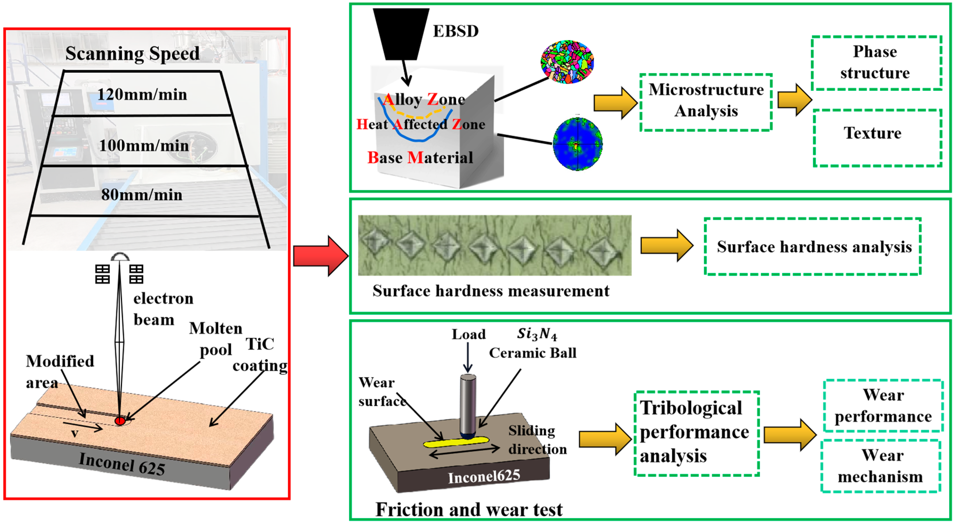
2. Materials and Methods

Figure 1 shows the experimental flowchart of this study. To begin, a vacuum electron beam welding machine scanned the electron beam of the nickel-base alloys. Secondly, EBSD experiments were carried out on the cross-section of the treated material to analyze the evolution of its microstructure. Then, the surface of the material was tested for microhardness. Finally, the friction and wear experiment on the surface was carried out to explore its wear properties and wear mechanism.

2.1. Sample Preparation

Inconel 625 nickel-base alloy was used as the base material in this study (the main components are shown in Table 1), and TiC powder (particle size 2–4 μm) was an additive. Using the Electrical Discharge Machining (EDM), the nickel-base alloy was cut into 100 mm × 100 mm × 10 mm alloy samples. First, polyvinyl alcohol was added at 2% (mass fraction) into the TiC powder and was wet with 65 °C warm water. It was evenly coated on the surface of the Inconel 625 substrate. The coating thickness was 0.3 mm, and it was measured with a micrometer after each application to ensure that the coating thickness was consistent. Finally, it was placed in a 120 °C drying oven and baked for 30 min for electron beam surface modification.

2.2. Electron Beam Surface Alloying Treatment

In this test, the Inconel 625 nickel-base alloy was surface alloyed (EBSA) with vacuum electron beam scanning, as shown in Figure 1. As shown in Table 2, under the premise of keeping other parameters unchanged, the scanning speed was changed to explore its influence on the microstructure and mechanical properties of the nickel-base alloy. Under the action of the magnetic lens, the electron beam forms a focused near beam. Through the movement of the electron gun, the electron beam current carries out surface treatment at the preset scanning track and scanning speed. According to the different scanning speeds, the samples were marked as C80, C100, and C120. The original specimen was marked as the base metal material (BM).

2.3. Microhardness and Friction and Wear Test

The microhardness of the alloy layer surface was measured with a Vickers hardness tester (HV, Huayin, China, HVS-1000) with a load of 3 N and a loading time of 15 s. Each position was repeated three times to reduce the error.
Using the Electrical Discharge Machining (EDM), the sample was cut into a 20 mm × 20 mm × 10 mm square. The friction and wear test was conducted at dry room temperature using the reciprocating sliding friction and wear module of the RTEC (MFT-5000) friction and wear tester. A YG10 tungsten steel ball with a diameter of 6.35 mm was selected as the friction pair. Before the test, the surface of the specimen was ground and polished to keep the roughness of all the specimens within Ra 0.05 mm. The test sliding speed was 12 mm/s, the stroke was 12 mm, the normal load was 50 N, the contact form of the friction pair was a spherical point contact, and the friction mode was linear reciprocating motion. The sliding time was 30 min. Under the dry friction condition, the test was started by stably clamping the sample onto the test platform. Before and after each test, the sample and test platform was cleaned with absolute ethanol to avoid the impact of wear debris left from the previous test on the subsequent test results.
The three-dimensional (3D) surface profiler based on white light interferometer scanning was used to measure the three-dimensional topography of the wear surface. The Gwyddion image analysis software was used to calculate the wear volume. In order to reduce the error, each group of tests was repeated three times, and the results were averaged. The (ZIESS SIGMA FE-SEM (ZIESS, Jena, Germany)) scanning electron microscope equipped with an energy dispersive spectrometer (EDS) was used to observe and analyze the morphology and chemical composition of the worn surface of Inconel 625.

2.4. Microstructure Characterization Test

The samples for electron backscatter diffraction (EBSD) were finely mechanically polished with diamond powder and electropolished for 20 s under 10 V of voltage in a 100 mL perchloric acid solution. The scanning electron microscope (SEM, Zeiss Sigma300, Germany) equipped with an EBSD sensor (Oxford Instrument, Abingdon, UK) was applied in a distance of 0.8 μm of the step size to capture the original data, and commercial Channel5 software was used to analyze the data.

3. Results and Discussion

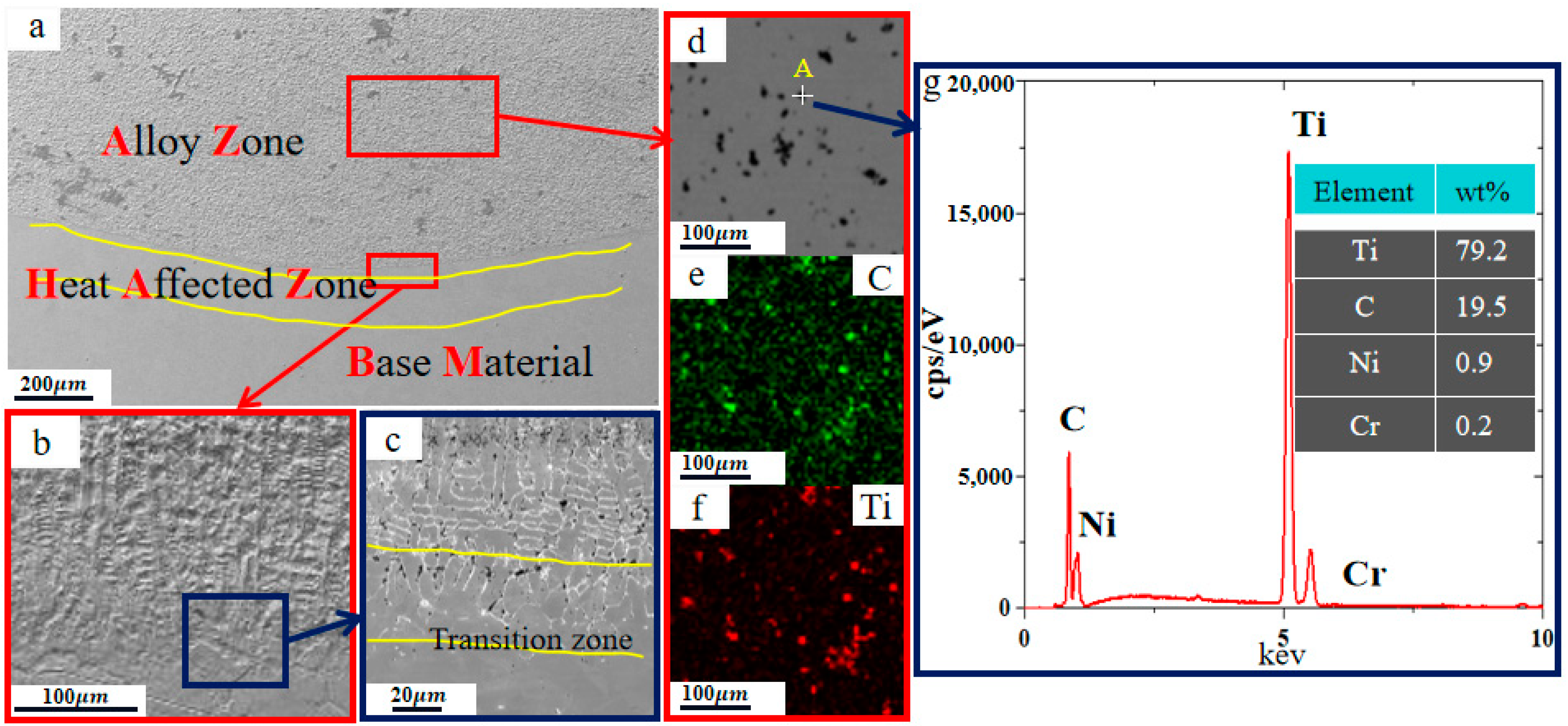
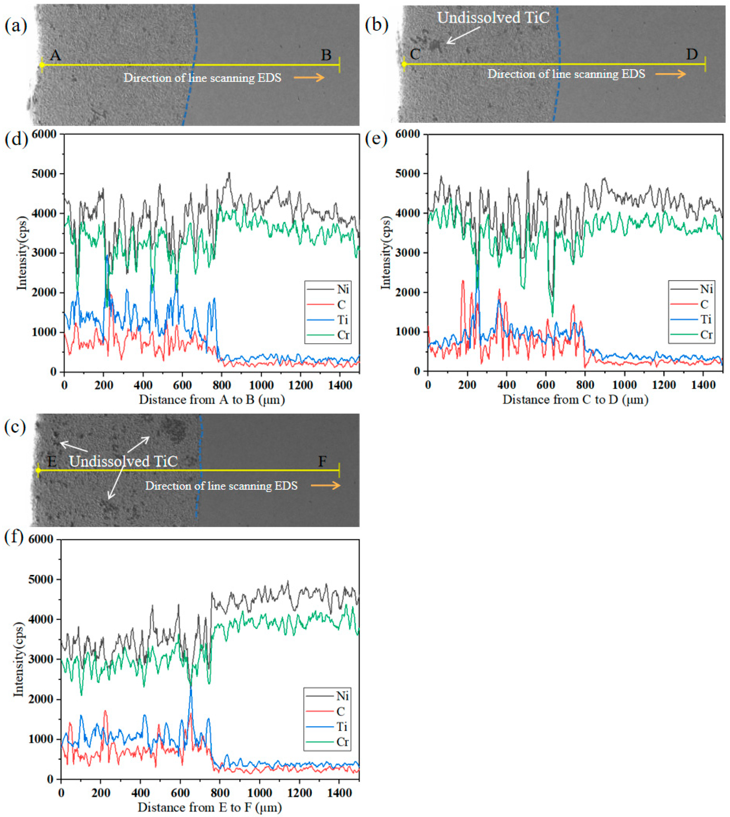
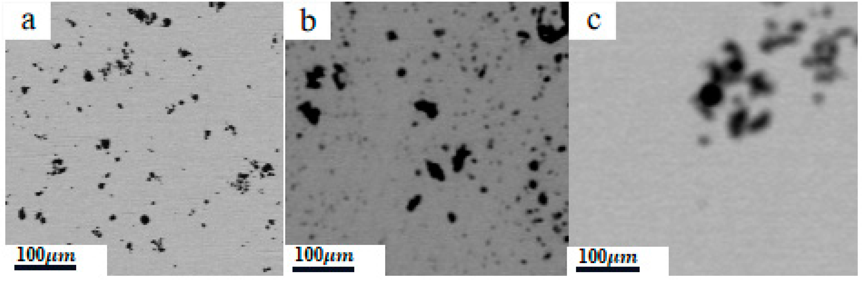
3.1. Microstructure Analysis

Figure 2 shows the SEM morphology and EDS results of the cross-section of the alloy area at the scanning speed of 80 mm/min. On the macroscale, three subregions are selected on the sample section as shown in Figure 2a, including the base metal (BM), heat-affected zone (HAZ), and alloy zone (AZ). Obviously, the microstructure of the alloy zone has changed after adding the TiC powder. Figure 2b shows a rapid directional solidification structure around the bonding area between the alloy layer and the substrate, and the growth direction of the columnar crystal is perpendicular to the interface. As can be seen in Figure 2c, there is a narrow transition zone between the alloy layer and the base metal. This is related to the undercooling solidification parameters, specifically the thermal gradient (G) and solidification rate (R) [28,29]. The bonding zone between the alloy layer and the substrate has a very large G and a very small R. As a result, because G/R tends to infinity, planar crystals grow from the substrate. Through the backscatter image, Figure 2d, it can be seen that granular TiC is uniformly distributed in the alloy layer with a volume fraction of approximately 12%. Interestingly, some particles appear in the alloy layer, and the measured particle size is approximately 8–15 μm. The results of the EDS (Figure 2e,f) show that the content of Ti and C elements is significantly higher than that of other elements. Figure 2g shows the scanning results for point A, and strong peaks for Ti and C can be observed. The content of the Ti element is 79.2 wt%, and the content of the C element is 19.5 wt%. Taking into account the EDS spectra and quantification, it can be reasonably inferred that the particles are TiC. P.F. Jiang et al. found a similar phenomenon in the preparation of TiC-reinforced, high-entropy alloy coatings with laser surface alloying [30].
Figure 3a–f shows the cross-sectional morphology and element distribution of the alloy layer interface. It can be clearly seen that a narrow transition zone appears at the interface between the alloy zone and the base material, achieving good metallurgical bonding between the base and the alloy layer. This is consistent with the phenomenon observed in Figure 2c. For Figure 3d–f, the element content changes significantly from the alloy layer to the interior of the substrate, especially in the transition zone. It can be judged from the EDS results that the elements are fully diffused in the molten pool during the process of EBSA. This is mainly due to the extremely high energy-conversion rate in the process of the scanning electron beam surface treatment. It can be seen that, for the 80 mm/min sample, the Ti and C elements in the alloy area are higher than the other two samples. This may be attributed to the phenomenon of “powder blowing” during electron beam scanning. That is to say, the scanning speed of 100 mm/min and above blow away TiC particles and affect their fusion with Inconel 625. With the increase in scanning speed, the heating time of the TiC powder on the surface becomes shorter, and the phenomenon of powder splash is more serious, which leads to a reduction in the content of Ti and C elements in the alloy area. The aggregation of the partially unmelted TiC can also be seen in Figure 3b,c. Based on the above analysis results, it is concluded that a good TiC coating can be prepared with electron beam surface alloying.
In order to study the grain morphology and optimize the growth orientation and related crystal structure, the alloy layer was further characterized with EBSD. Figure 4 shows the IPF, recrystallization, and KAM images of the alloy area at different scanning rates.
The matrix grains are mainly austenite equiaxed grains with an average size of approximately 20 microns accompanied by a large number of straight twins (Figure 4a). The grain orientation is relatively dispersed, and there is no obvious preferential orientation. There are mainly island grains and no columnar particles in the 80 mm/min sample [31]. The average grain size is approximately 45 μm. This is due to the fact that the TiC points are dispersed, and the heat flow distribution is relatively more uniform. Figure 4d shows that there are few columnar crystals in the microstructure. They are uniformly distributed and have fine equiaxed crystal structures [32]. When the scanning speed reaches 100 mm/min, the grains in the microstructure of the alloy layer become larger; however, it is still dominated by island grains, and the average grain size is approximately 70 μm (Figure 4h). With the increase in scanning speed, a large number of columnar crystals appear in the microstructure of the alloy layer, and the average grain size is approximately 90 μm (Figure 4k). It can be observed that the TiC particles are preferably formed at grain boundaries, and the pinning effect caused by TiC precipitation around the grain boundary leads to a limited grain growth process. Therefore, the introduction of TiC into nickel-base alloys can play a role in grain refinement.
Figure 4b,e,h,k shows the recrystallization images of the nickel-base alloy microstructure under EBSA treatment at different scanning speeds. The red represents the deformation area, the blue represents the recrystallization area, and the yellow represents the substructure area. The original sample has a large distortion area and a small amount of recrystallization area. However, after EBSA treatment, the distortion area of the sample is reduced. The area of yellow substructure gradually increases. This is mainly because the material surface rapidly heats up and melts, and recrystallization occurs in the process of EBSA. However, due to the extremely high cooling rate, some grains do not complete recrystallization and remain in the substructure stage. In addition, with the increase in scanning speed, the blue recrystallization area increases significantly. This may be due to the increasingly serious phenomenon of “powder blowing” caused by the increase in scanning speed, fewer low-temperature TiC points dispersed in the alloy area, more concentrated heat flow, and more complete recrystallization.
The KAM image is a qualitative representation of the degree of non-uniformity of material molding deformation and defect density distribution with the help of the kernel average misorientation algorithm in EBSD. The grain substructure and reaction strain are studied through the kernel average misorientation (KAM) measured with EBSD. The KAM image shows different areas of poor orientation in the sample with different colors reflecting the degree of strain concentration. The red area in the image represents the area with a large orientation difference in the grain, that is, the area with high strain concentration, while the opposite blue area represents the area with low strain concentration.
Figure 4c,f,i,l shows the KAM images of the microstructure of a nickel-base alloy treated with EBSA at different scanning speeds. The overall dislocation density of the original sample is high, and there is a high concentration of dislocation defect density in the local area. The overall dislocation density of the EBSA-treated samples is low, and only some grain boundaries have a high dislocation defect density. In addition, with the increased scanning speed and recrystallization degree, the dislocation defect density tends to decrease, and there is basically no high KAM value at 120 mm/min. The results show that EBSA treatment can reduce the stress concentration in the subsurface layer.

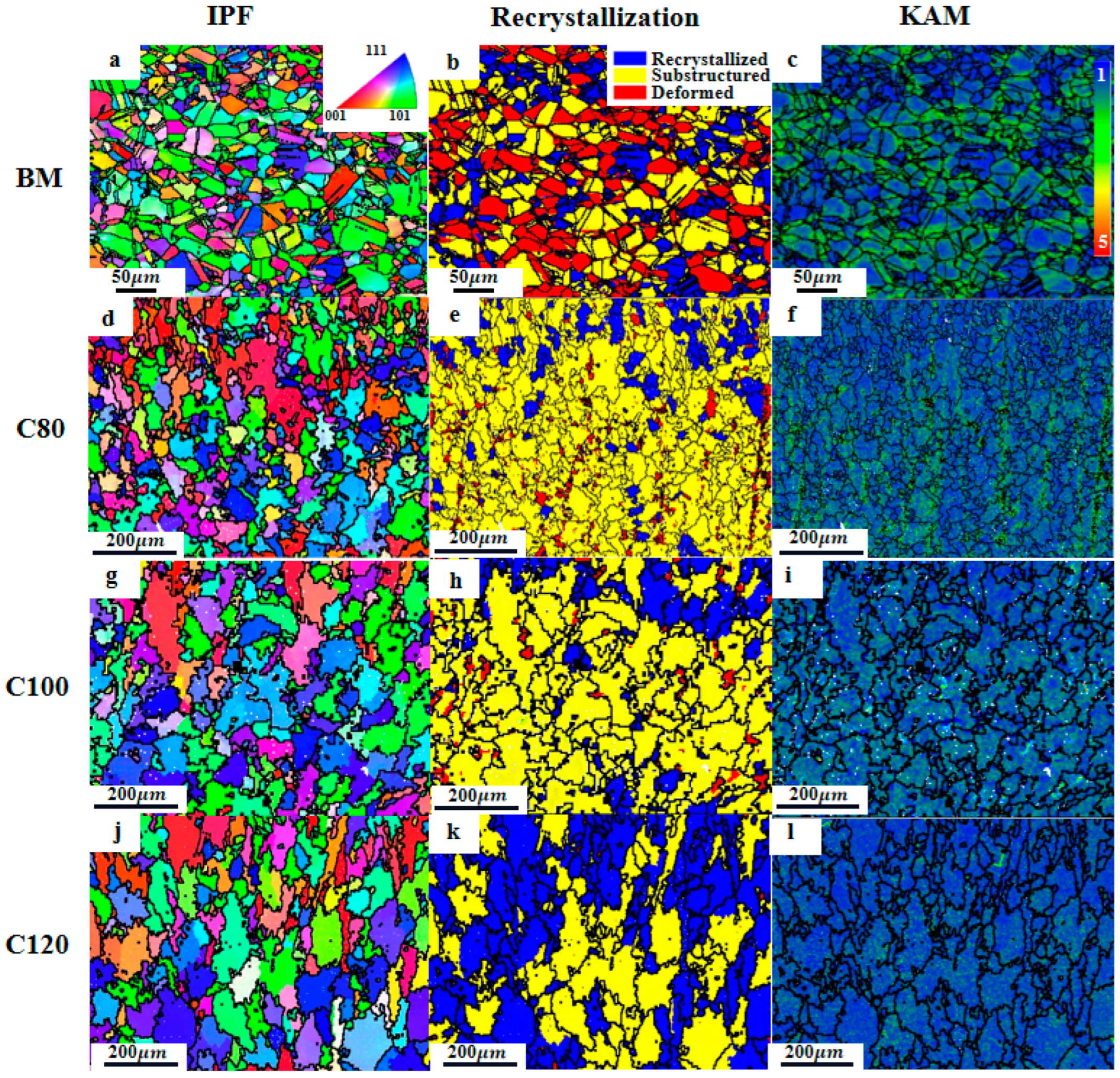
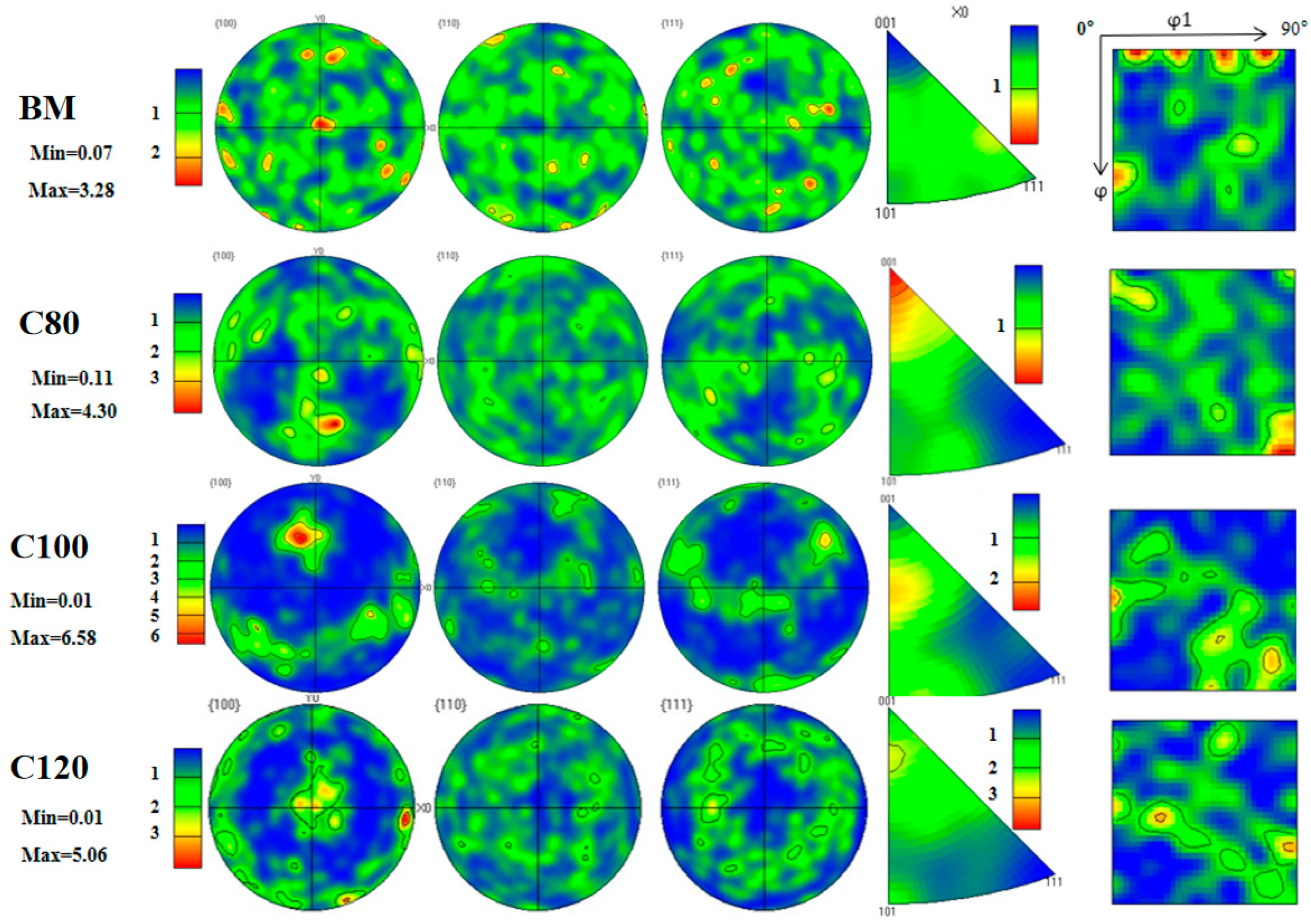
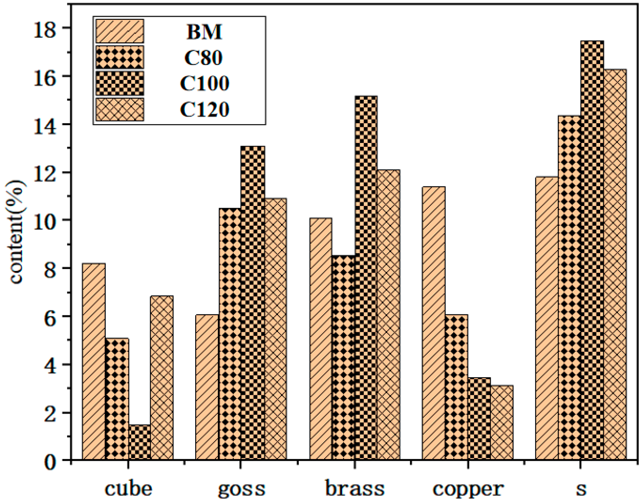
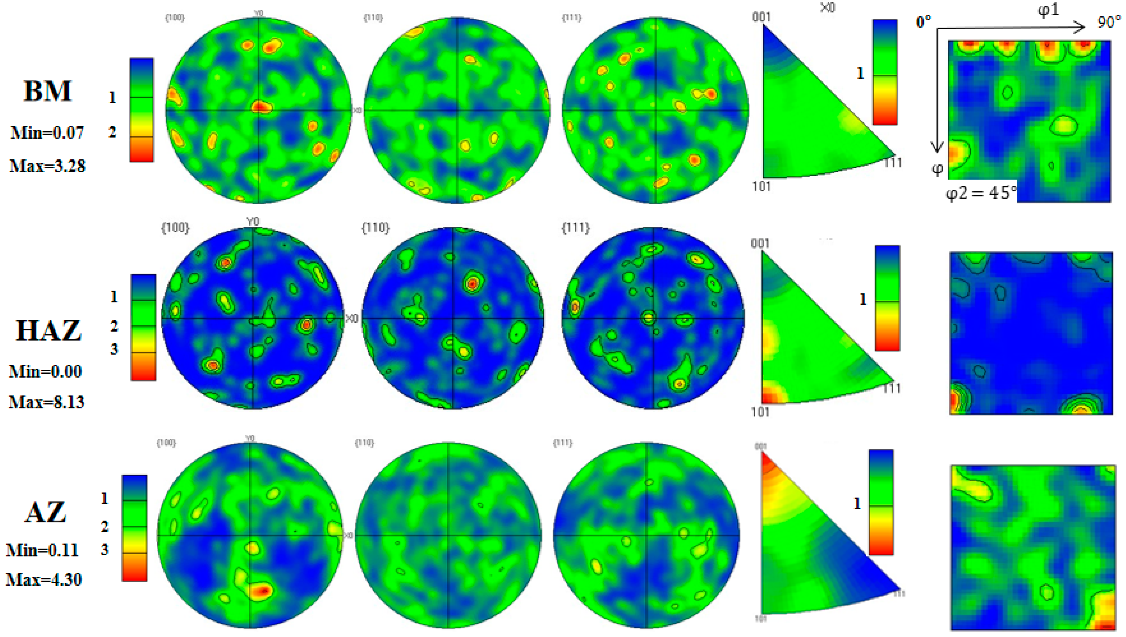
3.2. EBSD Texture Analysis

Figure 5 depicts the original Inconel 625 sample as well as the sample after electron beam surface alloying from 80 mm/min to 120 mm/min, as well as the ODF screenshot (φ2 = 0°, 45°, 60°). The Euler angle is obtained from the ODF intercept graph and then converted into the corresponding plate texture to represent the distribution of the austenite texture. According to Figure 5, the austenite texture is relatively dispersed but primarily concentrated in the Copper{112}<111> and S{123}<634> with a trace of Brass{110}<112> and Rotated Cube{001}<110>. When the scanning speed is 80 mm/min, the texture orientation becomes concentrated, mainly focusing on the Brass{110}<112> and S{123}<634> texture orientations. With the scanning speed increasing to 100 mm/min, the preferred orientation of the grains is further enhanced, and the textures are concentrated in Brass{110}<112> and S{123}<634> textures accompanied by Goss{011}<100> textures of a certain strength. When the scanning speed is 120 mm/min, the texture intensity is weakened, and the texture mainly focuses on the Brass{110}<112> and S{123}<634> texture orientations. After EBSA treatment, the Copper{112}<111> texture is significantly weakened, while the Goss{011}<100> texture and the S{123}<634> texture are significantly enhanced. When the scanning speed reaches 100 mm/min, the Goss{011}<100> texture and S{123}<634> texture strength reach the highest value.
Figure 6 shows the content of the austenite texture in the original Inconel 625 sample and the sample in the AZ area after 80–120 mm/min EBSA treatment. It can be seen from Figure 6 that the texture distribution of the original sample is relatively dispersed. Under different scanning speeds, the austenitic texture types change to some extent but eventually form the enhanced Goss{011}<100> and S{123}<634> textures. Therefore, the structure is mainly S texture {123}<634> accompanied by Goss {011}<100> and Brass {110}<112> with a certain strength.
Figure 7 is the ODF image of the FCC phase in different areas of the Inconel 625 original sample after 80 mm/min EBSA treatment. It can be seen from the figure that FCC also has some textures in the BM part. These textures are relatively dispersed with Cube{001}<100>, Rotated Cube{001}<110>, and Copper{112}<111> textures, and S{123}<634> textures. In the HAZ area, a strong texture is formed, concentrated on the {101} plane with Rotated Cube{001}<110> and Rotated Goss{011}<110>. In the AZ area, certain textures are also formed in the austenite, and these texture components are mainly Goss{110}<001> and S{123}<634> textures accompanied by a certain strength of the Rotated Cube{001}<110> texture. This is mainly because there are a large number of TiC particles in the AZ region. It leads to more complex heat flow directions during the EBSA process and weakens the formation of the texture. X. Cui, X. Wang, et al. found similar phenomena in previous studies [33,34].

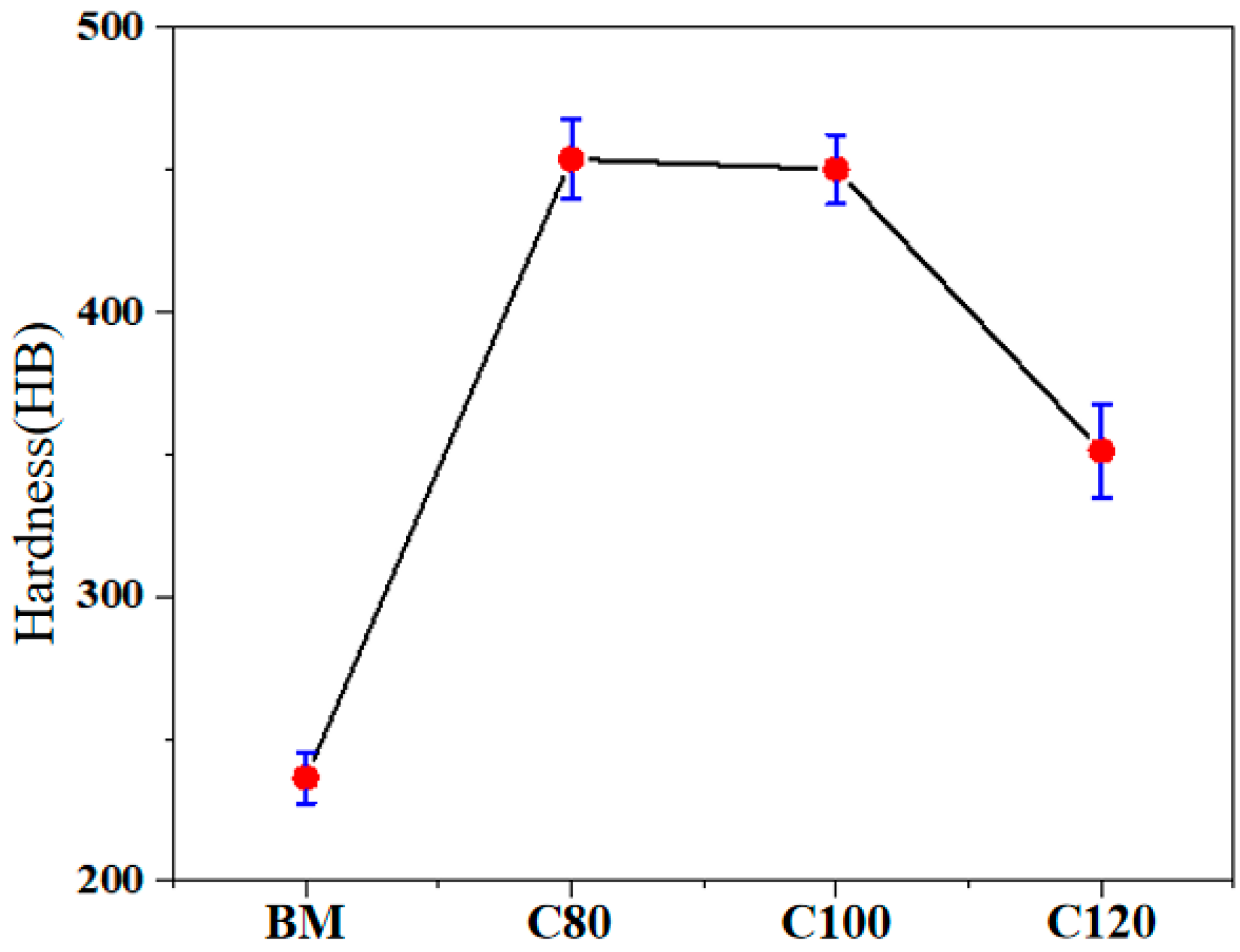
3.3. Microhardness Analysis

Figure 8 shows the microhardness of the surface at different scanning speeds. It can be seen that the surface hardness of the material after EBSA is higher than that of the base material (236 HB) and reaches the maximum value of 457 HB in C80, 1.936 times that of the base material. The microhardness decreases with the increase in scanning speed. This is because with the increase in the scanning speed, the “powder blowing” phenomenon in the EBSA process becomes more serious, resulting in the decrease in the TiC hard phase in the AZ alloy layer and the decrease in the surface hardness. It can be noted that the microhardness of 80 mm/min differs greatly from that of 120 mm/min, which may also be related to internal defects and non-uniform microstructures in local areas. Similar phenomena were also found in the research of Zhou et al. [35]. In addition, the results show that TiC strengthening particles play an active role in improving the microhardness of nickel-base alloys. The improvement in microhardness of the TiC coatings can be explained by the following two aspects: on the one hand, the TiC particles that precipitated in the alloy layer serve as the strengthening phase distributed in the solid solution phase, and the increase in the TiC particle volume fraction leads to a higher dispersion strengthening contribution. On the other hand, the TiC powder refined the grains of the alloy layer [36].
Figure 9 shows the backscattering images of the specimens at different scanning speeds. The TiC particles are relatively small and evenly distributed in the C80 image. As the scanning speed increases to 100 mm/min, the size of the TiC particles increases to 30 µm, and the TiC particles become unevenly distributed. In the C120 image, partial TiC enrichment occurred. This is because the too fast scanning speed makes some TiC “splash”. This may also be the reason for the reduced surface hardness and large fluctuations in the surface hardness of C120.

3.4. Analysis of Friction and Wear Behavior

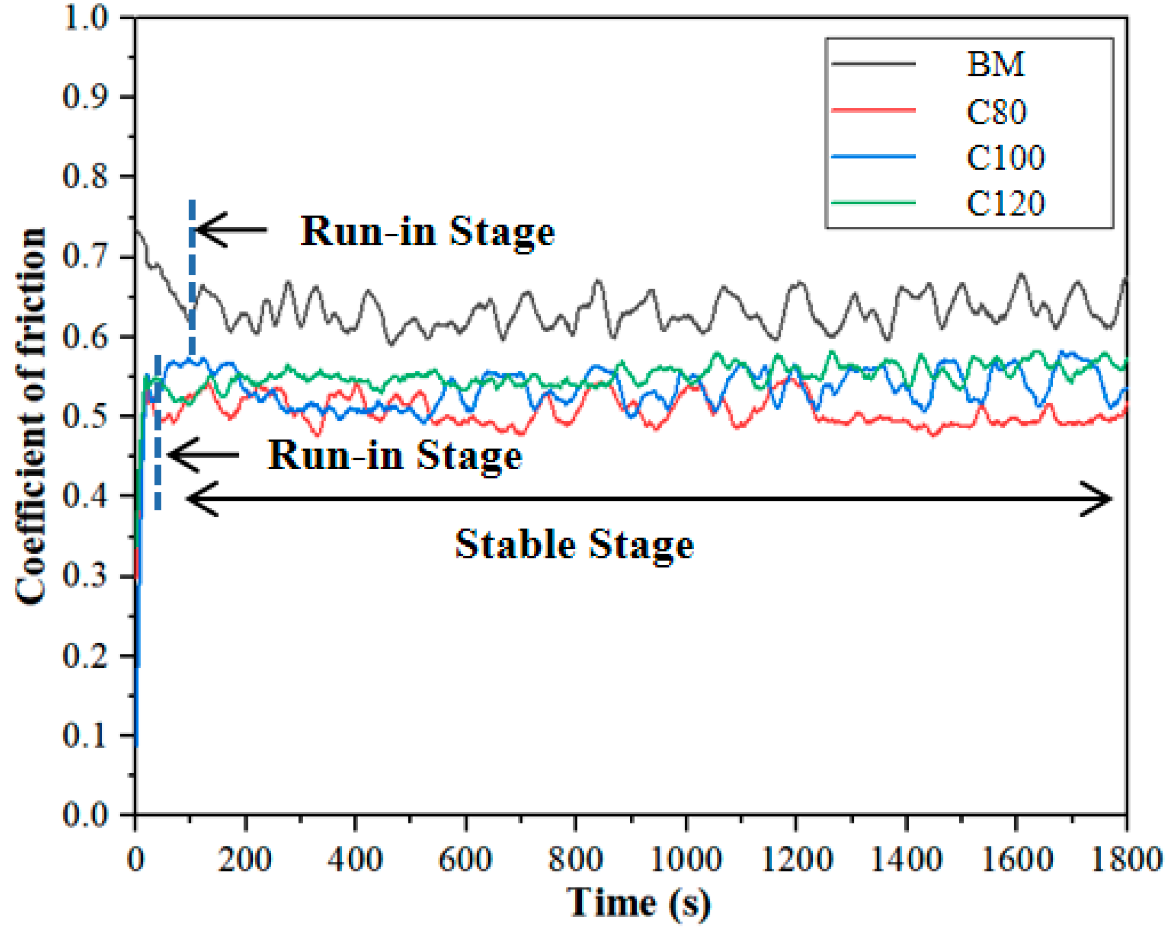
3.4.1. Friction Coefficient

Figure 10 shows the friction coefficient–time curves of the test specimens at different scanning speeds. The coefficient of friction increases rapidly during the operating phase, then gradually decreases and stabilizes after a period of time, entering the stabilization phase. Among them, the running-in time of the base metal is significantly higher than that of other materials. It can be seen that the friction coefficient of the base material fluctuates approximately 0.63 in the stable stage, while the friction coefficient of the sample after EBSA treatment is lower than that of the base material and fluctuates between 0.5 and 0.57. The decrease in the average friction coefficient of the sample surface after EBSA treatment is due to the TiC strengthening phase increasing the surface hardness of the material [37]. In addition, the friction coefficient increased slightly with the increase in scanning speed in the later stage of the test. This may be due to the decrease in the TiC content deposited on the substrate surface with the increase in scanning speed.

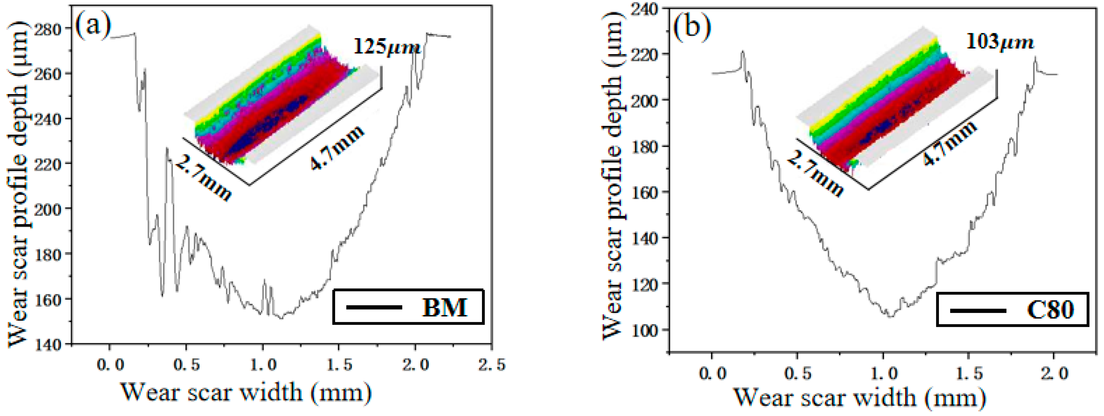
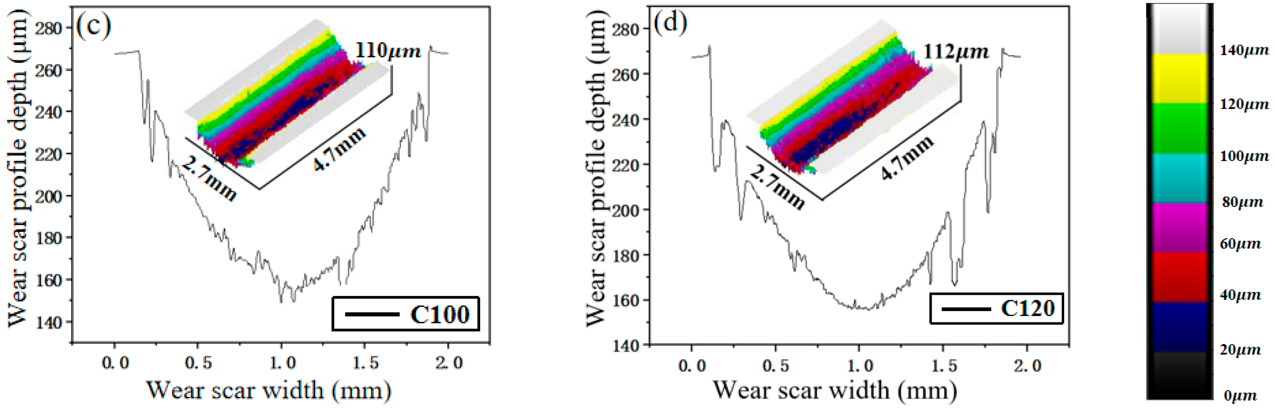
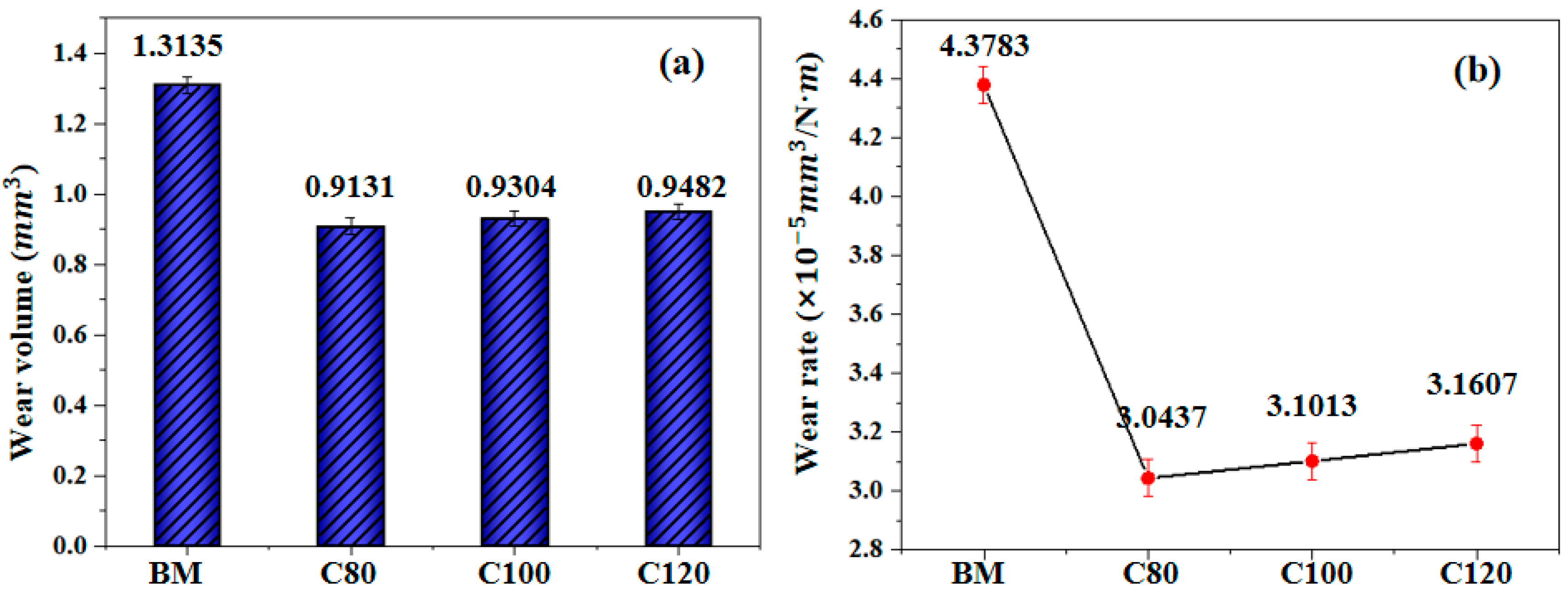
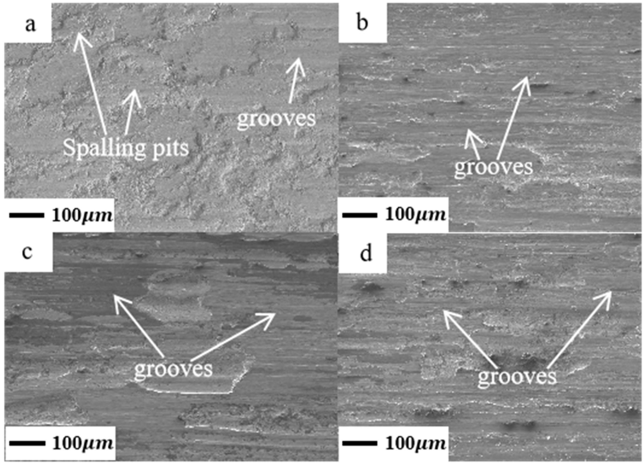
3.4.2. Macro Morphology of Wear Scar, Wear Volume, and Wear Rate

After the friction and wear test, a three-dimensional (3D) surface profiler based on white light interferometer scanning was used to measure the three-dimensional morphology of the worn surface of the sample. Figure 11 shows the three-dimensional morphology and wear-scar section curve of the sample’s worn surface under the same load and different scanning speeds. It can be seen that the substrate material is most severely worn with the largest width and depth of wear marks reaching 125 μm at the deepest point. The wear of the EBSA-treated samples was improved. According to the different wear macro-morphologies, the process parameters have a greater impact on the wear scar. The maximum wear depth increases with the increase in scanning speed. The depth of the wear scar in the 80 mm/min sample is the minimum, and the depth of the wear scar is 103 μm. The depth of the wear scar in the 120 mm/min sample is the largest, and the depth of the wear scar is 112 μm.
The wear volume was calculated with Gwyddion image analysis software. The formula for calculating the wear rate is:
W = V/F·S
where W represents the wear rate ( m m 3 / ( N · m ) ), V represents the wear volume ( m m 3 ), F represents the normal load (N), and S represents the sliding distance ( m ). As shown in Figure 12, the minimum wear volume at 80 mm/min is 0.9131 m m 3 , and the maximum wear volume at the matrix is 1.3135 m m 3 . Compared with the matrix, the 80 mm/min wear volume decreased by 30.48%. The minimum wear rate at 80 mm/min is 3.0437, and the maximum wear rate of the matrix is 4.3783. Compared with the matrix, the wear rate of the 80 mm/min sample also decreased by 30.48%.
Figure 13 presents the wear profile of the test specimens with SEM. The original specimen wear surface is distributed with different shades and areas of spalling pits. This reflects the mechanism of fatigue wear. A thin and shallow furrow parallel to the sliding direction indicates weak abrasive wear. The abrasive particles around the spalling pit increase, and the abrasive wear increases; therefore, obvious cracks and spalling pits can be observed in Figure 13a, and the surface roughness increases. However, in Figure 13b–d, the pear groove was more obvious, and no large-scale spalling pits were observed; this indicates a decrease in the fatigue wear of the material. During the wear process, the degree of wear of the TiC alloy layer alloyed on the surface of the vacuum electron beam is reduced. This phenomenon is due to the pinning effect near the grain boundary, which improves the performance of the material. In addition, the uniform fine structure gives the coating good toughness and strength and good anti-delamination and peel resistance [38,39]. Therefore, the reinforced phase of the TiC can give full play to its wear resistance in nickel-base alloys.

4. Conclusions

The Inconel 625 nickel-base alloy was treated with vacuum electron beam surface alloying with a TiC coating at different scanning speeds, and the effects of the scanning speeds on the microstructure and wear properties were studied. The results are as follows:
(1) In the process of EBSA, the elements fully diffused in the molten pool. This was mainly due to the extremely high energy-conversion rate in the process of the scanning electron beam surface treatment. It could be seen that the 80 mm/min sample and alloy area Ti and C elements were higher than the 100 mm/min and 120 mm/min samples. The scanning speed of 100 mm/min and above blew away TiC particles and affected their fusion with Inconel 625. With the increase in the scanning speed, the heating time of the TiC powder on the surface became shorter, and the powder splash was serious. Then, the content of Ti and C in the alloy zone decreased, and the aggregation of the partially unmelted TiC could be seen. A good TiC coating was prepared with electron beam surface alloying.
(2) The C80 sample mainly contains island particles with an average grain size of approximately 45 μm. There are a few fine equiaxed columnar crystals in the microstructure. This is because the TiC particles are dispersed in it, and the heat flow distribution is relatively uniform. When the scanning speed reached 100 mm/min, the grains in the microstructure of the alloy layer became larger, still dominated by island grains, and the average grain size was approximately 70 μm. When the scanning speed reached 120 mm/min, the grains in the microstructure of the alloy layer became larger, and a large number of columnar crystals appeared with an average grain size of 90 μm.
(3) The austenite texture in the original sample was relatively dispersed, focusing primarily on the Copper {112}<111> and S {123}<634> textures with a trace of Brass {110}<112> and Rotated Cube {001}<110>. When the scanning speed was 80 mm/min, the texture orientation became concentrated, mainly focusing on the Brass {110}<112> and S {123}<634> texture orientations. The preferred orientation of the grains was further enhanced in the C100 sample, and the textures were concentrated in Brass {110}<112> and S {123}<634> accompanied by Goss {011}<100> textures of a certain strength. When the scanning speed was 120 mm/min, the texture intensity was weakened, and the texture mainly focused on the Brass {110}<112> and S {123}<634> texture orientations. After EBSA treatment, the Copper {112}<111> texture was significantly weakened, while the Goss {011}<100> texture and the S {123}<634> texture were enhanced.
(4) The surface hardness of the material after EBSA was higher than that of the base material (236 HB) and reached the maximum value of 457 HB at 80 mm/min, 1.936 times that of the base material. Because the TiC strengthening phase made the surface hardness of the material increase, the average friction coefficient of the surface decreased. With the increase in scanning speed, the decrease in TiC content deposited on the substrate surface led to a decrease in hardness and a slight increase in the friction coefficient. The minimum wear volume was 0.9131 m m 3 at 80 mm/min, and the maximum wear volume was 1.3135 m m 3 at the matrix. Compared with the matrix, the 80 mm/min wear volume decreased by 30.48%. During the wear process, the wear degree of the TiC alloy layer alloyed on the surface of the vacuum electron beam decreased. This was because the pinning effect near the grain boundary enhanced the properties of the material. In addition, the uniform fine structure of non-equilibrium solidification made the coating have good toughness and strength and good anti-delamination and anti-stripping properties.

Author Contributions

J.Y.: Conceptualization, Methodology, Investigation, Writing—original draft. J.L. (Juan Li): Conceptualization, Validation, Investigation, Writing—review and editing, Visualization, Supervision. G.Z.: Investigation, Writing—review and editing, Supervision. H.L.: Conceptualization, Writing—review and editing, Visualization. L.M.: Investigation, Writing—original draft, Formal analysis. J.L. (Jie Liu): Investigation. All authors have read and agreed to the published version of the manuscript.

Funding

The project was supported by the Fundamental Research Program of Shanxi Province (20210302123207 and 20210302124009), Scientific and Technological Innovation Programs of Higher Education Institutions in Shanxi (2021L292), Taiyuan University of Science and Technology Scientific Research Initial Funding (20212026), Taiyuan University of Science and Technology Graduate Innovation Project (BY2022004 and SY2022088), and the Coordinative Innovation Center of Taiyuan Heavy Machinery Equipment.

Data Availability Statement

All the data corresponding to the research are presented in the articles in Tabular or in graphical form.

Acknowledgments

The authors would like to thank Shanxi Provincial Key Laboratory of Metallurgical Device Design Theory and Technology for providing financial support for this research.

Conflicts of Interest

The authors declare that they have no known competing financial interest or personal relationships that could have appeared to influence the work reported in this paper.

References

  1. Hill, A.J.; Mardel, I.; Sare, I.R. Wear-resistant metallic and elastomeric materials in the mining and mineral processing industries-an overview. Wear 2001, 250, 1–10. [Google Scholar]
  2. Huiyang, W.; Yunqi, A.; Chengyu, L.; Bing, C.; Ya, N.; Guobin, L.; Ping, L. Research progress of nickel-base superalloy materials. Mater. Guide 2011, 25, 482–486. [Google Scholar]
  3. Jianting, G. Superalloy Materials; Science Press: Beijing, China, 2010. [Google Scholar]
  4. Rajani, H.; Mousavi, S. The Role of Impact Energy in Failure of Explosive Cladding of Inconel 625 and Steel. J. Fail. Anal. Prev. 2012, 12, 646–653. [Google Scholar] [CrossRef]
  5. Yuchun, L.; Lian, C.; Xuegang, Z.; Liang, S.; Jixin, C. Preparation of Co-Al composite coating on nickel-base superalloy. J. Nat. Sci. Harbin Norm. Univ. 2018, 34, 84–87. [Google Scholar]
  6. Deqiang, W.; Xulong, R.; Rong, W.; Shaopeng, L. Microstructure and hardness of the surface of W-alloyed 45 steel by electron beam scanning. J. Weld. 2019, 40, 98–103. [Google Scholar]
  7. Binggang, Z.; Jian, Z.; Jicai, F. Electron beam surface alloying research progress. J. Weld. 2011, 32, 108–112. [Google Scholar]
  8. Jianglong, L.; Zhirong, Z.; Bao, S. Reject High-Energy Beam Heat Treatment, 1st ed.; China Machine Press: Beijing, China, 1997. [Google Scholar]
  9. Cai, J.; Lv, P.; Zhang, C.L.; Wu, j.; Li, C.; Guan, Q.F. Microstructure and properties of low carbon steel after surface alloying induced by high current pulsed electron beam. Nucl. Instrum. Methods Phys. Res. Sect. B Beam Interact. Mater. At. 2017, 410, 47–52. [Google Scholar] [CrossRef]
  10. Yang, S.; Guo, Z.; Zhao, L.; Guan, Q.; Zhao, L.; Liu, Y. Microstructures and corrosion resistance of Zircaloy-4 after surface alloying with copper by high-current pulsed electron beam. Appl. Surf. Sci. 2020, 501, 144222. [Google Scholar] [CrossRef]
  11. Petrov, P. Electron beam surface remelting and alloying of aluminium alloys. Vacuum 1997, 48, 49–50. [Google Scholar] [CrossRef]
  12. Zhexuan, Z.; Zaifeng, Z.; Quan, S.; Zulai, L.; Yehua, J.; Fei, Z. Effect of Surface Tungsten Alloying on Microstructure and Hardness of High Chromium Cast Iron. Mater. Guide 2019, 33, 362–365. [Google Scholar]
  13. Balachandran, G.; Menaka, K.; Ravichandar, D. Influence of Manganese and Boron Alloying and Processing Conditions on the Microstructure and the Mechanical Properties of 0.4% Carbon Steels. Trans. Indian Inst. Met. 2019, 72, 401–409. [Google Scholar] [CrossRef]
  14. Anjos, S.D.; Da Costa, F.H.; Sallica-Leva, E.; Caram, R.; Amigó, V.; Fogagnolo, J.B. Laser surface alloying applied on Ti3Mo and Ti-10Nb sintered parts. Surf. Coat. Technol. 2021, 407, 126773. [Google Scholar] [CrossRef]
  15. Bartkowski, D.; Młynarczak, A.; Piasecki, A.; Dudziak, B.; Gościański, M.; Bartkowska, A. Microstructure, microhardness and corrosion resistance of Stellite-6 coatings reinforced with WC particles using laser cladding. Opt. Laser Technol. 2015, 68, 191–201. [Google Scholar] [CrossRef]
  16. Wei, D.; Zhang, P.; Yao, Z.; Chen, X.; Li, F. Double glow plasma surface Cr-Ni alloying of Ti6Al4V alloys: Mechanical properties and impact of preparing process on the substrate. Vacuum 2018, 155, 233–241. [Google Scholar] [CrossRef]
  17. Wang, Q.; Zhao, Z.; Bai, P.; Du, W.; Liao, H.; Li, Y.; Liang, M.; Huo, P.; Zhang, L.; Tie, D. Effects of alloying elements X (Cr, Mn, Mo, Ni, Si) on the interface stability of TiC (001)/γ-Fe (001) in TiC/316L stainless steel composite formed by selective laser melting: First principles and experiments. Adv. Compos. Hybrid Mater. 2021, 4, 195–204. [Google Scholar] [CrossRef]
  18. Ren, X.; Wang, R.; Wei, D. The microstructure and properties of Cr/Ni alloying layer after surface alloying treatment induced by continuous scanning electron beam process. J. Phys. Conf. Ser. 2021, 1820, 012144. [Google Scholar] [CrossRef]
  19. Longzhang, Z.; Qingyuan, Z.; Yufei, C.; Bo, H.; Yan, Z. Study on electrodeposition of nickel cobalt tungsten carbide composite coating. Electroplat. Finish. 1999, 1, 4–7. [Google Scholar]
  20. Bo, H.; Jialiang, Z.; Jiaojiao, L. Microstructure and wear resistance of laser cladding tungsten carbide/cobalt-based alloy composite coating. Appl. Laser 2017, 37, 314–318. [Google Scholar]
  21. Ru, J.; Wang, Y.; Zhou, Y.; Jiang, Z.; Xu, X.; Li, J. Effect of Si on the Microstructure and Oxidation Resistance of Ti-Mo Alloys. JOM 2020, 72, 354–360. [Google Scholar] [CrossRef]
  22. Lass, E.A. The effects of Fe and Si on the phase equilibria in a γ’-strengthened Co–Al–W-based superalloy. J. Alloy. Compd. 2020, 825, 154158. [Google Scholar] [CrossRef]
  23. Mankui, Z.; Guifang, S.; Wei, Z.; Weixiang, L.; Kun, W. Investigation of the corrosion of the Cr-CrB2 laser alloying layer on stainless steel surfaces. Laser Technol. 2014, 38, 240–245. [Google Scholar]
  24. Huang, S.W.; Nolan, D.; Brandt, M. Pre-placed WCy Ni clad layers produced with a pulsed Nd:YAG laser via optical fibres. Surf. Coat. Technol. 2003, 9, 26–34. [Google Scholar] [CrossRef]
  25. Deqiang, W.; Xinkai, L.; Xulong, R. Progress in surface modification research using an electron beam. Hot Work. Technol. 2016, 45, 19–23. [Google Scholar]
  26. Song, W.; Hui, L.; Hongbin, X.; Yong, C. Research progress on surface alloying based on high energy beams. South. Met. 2013, 5, 1–4. [Google Scholar]
  27. Fu, Z.; Fengjuan, W.; Jianjun, H.; Yuejin, M.; Aijun, M.; Jianchang, L. Three-beam surface modification technology application and development trends. Hebei Agric. Univ. J. 2003, 260–263+266. [Google Scholar]
  28. Nippes, E.F. The weld heat-affected zone. Weld. J. 1959, 38, 15–185. [Google Scholar]
  29. Kang, B.; Kong, T.; Ryu, H.J.; Hong, S.H. The outstanding tensile strength of Ni-rich high entropy superalloy fabricated by powder metallurgical process. Mater. Chem. Phys. 2019, 235, 121749. [Google Scholar] [CrossRef]
  30. Nair, A.M.; Muvvala, G.; Nath, A.K. A study on in-situ synthesis of TiCN metal matrix composite coating on Ti-6Al-4V by laser surface alloying process. J. Alloy. Compd. 2019, 810, 151901. [Google Scholar] [CrossRef]
  31. Jiang, P.F.; Zhang, C.H.; Zhang, S.; Zhang, J.B.; Chen, J.; Liu, Y. Fabrication and wear behavior of TiC reinforced FeCoCrAlCu-based high entropy alloy coatings by laser surface alloying. Mater. Chem. Phys. 2020, 255, 123571. [Google Scholar] [CrossRef]
  32. Cui, X.; Zhang, S.; Wang, C.; Zhang, C.H.; Chen, J.; Zhang, J.B. Effects of stress-relief heat treatment on the microstructure and fatigue property of a laser additive manufactured 12CrNi2 low alloy steel. Mater. Sci. Eng. 2020, 791, 139738. [Google Scholar] [CrossRef]
  33. Wang, X.; Zhang, C.H.; Cui, X.; Zhang, S.; Chen, J.; Zhang, J.B. Microstructure and mechanical behavior of additive manufactured Cr-Ni-V low alloy steel in different heat treatment. Vacuum 2020, 175, 109216. [Google Scholar] [CrossRef]
  34. Zhou, Y.; Chen, S.; Chen, X.; Cui, T.; Liang, J.; Liu, C. The evolution of bainite and mechanical properties of direct laser deposition 12CrNi2 alloy steel at different laser power. Mater. Sci. Eng. 2019, 742, 150–161. [Google Scholar] [CrossRef]
  35. Liu, H.; Liu, J.; Chen, P.J.; Yang, H.F. Microstructure and high temperature wear behaviour of in-situ TiC reinforced AlCoCrFeNi-based high-entropy alloy composite coatings fabricated by laser cladding. Opt. Laser Technol. 2019, 118, 140–150. [Google Scholar] [CrossRef]
  36. Zhang, H.; Zhang, C.; Wang, Q.; Wu, C.L.; Zhang, S.; Chen, J.; Abdullah, A.O. Effect of Ni content on stainless steel fabricated by laser melting deposition. Opt. Laser Technol. 2018, 101, 363–371. [Google Scholar] [CrossRef]
  37. Shuang, S.; Ding, Z.Y.; Chung, D.; Shi, S.Q.; Yang, Y. Corrosion resistant nanostructured eutectic high entropy alloy. Corros. Sci. 2020, 164, 108315. [Google Scholar] [CrossRef]
  38. Liu, J.; Liu, H.; Chen, P.J.; Hao, J.B. Microstructural characterization and corrosion behaviour of AlCoCrFeNiTix high-entropy alloy coatings fabricated by laser cladding. Surf. Coat. Technol. 2019, 361, 63–74. [Google Scholar] [CrossRef]
  39. Liu, Z.; Yang, P.; Li, X.; Wang, X.; Ma, J.; Liu, G. Formation of island grains in high-permeability grain-oriented silicon steel manufactured by the acquired inhibitor method. J. Phys. Chem. Solids 2020, 136, 109165. [Google Scholar] [CrossRef]
Figure 1. Experimental Flow Chart.
Metals 13 00275 g001
Figure 2. SEM morphology and EDS results of a cross-section of the alloy zone at C80: (a) SEM image; (b,c) Locally enlarged SEM image; (d) the backscatter image; (e,f) Results of EDS polygon scans; (g) A spot EDS point scan results.
Metals 13 00275 g002
Figure 3. Alloy zone (AZ) and heat-affected zone (HAZ) line scan images: (a,d) C80, (b,e) C100, (c,f) C120.
Metals 13 00275 g003
Figure 4. IPF, recrystallization, and KAM of Inconel 625 under EBSA treatment at different scanning speeds: BM (ac); C80 (df); C100 (gi); C120 (jl).
Metals 13 00275 g004
Figure 5. Corresponding pole image, reverse pole image, and ODF image of each area of the sample after 80 mm/min to 120 mm/min electron beam scanning (φ2 = 45°).
Metals 13 00275 g005
Figure 6. Austenite Texture Content of the Original Inconel 625 Sample and Specimens Treated with EBSA at Different Scanning Speeds.
Metals 13 00275 g006
Figure 7. Corresponding pole image, reverse pole image, and ODF image of each area of the sample after 80 mm/min electron beam scanning (φ2 = 45°).
Metals 13 00275 g007
Figure 8. Surface hardness of the specimens treated with EBSA at different scanning speeds.
Metals 13 00275 g008
Figure 9. The backscatter image of the specimens at different scanning speeds. (a) C80, (b) C100, (c) C120.
Metals 13 00275 g009
Figure 10. Friction coefficient–time curves of the test specimens.
Metals 13 00275 g010
Figure 11. Three-dimensional morphology and cross-section curve of the wear surface after EBSA treatment at different scanning speeds: (a) BM, (b) C80, (c) C100, (d) C120.
Metals 13 00275 g011aMetals 13 00275 g011b
Figure 12. Wear Results of the Nickel-Base Alloy at Different Scanning Speeds after EBSA: (a) Wear Volume; (b) Wear Rate.
Metals 13 00275 g012
Figure 13. The wear profile of the test specimens (a) BM, (b) C80, (c) C100, (d) C120.
Metals 13 00275 g013
Table 1. Inconel 625 chemical composition (mass fraction, %).
NiCrMoNbFeCNTiAl
61.922.88.43.42.20.90.10.10.1
Table 2. Electron beam scanning process parameters.
Beam
Current
Focusing CurrentAccelerating VoltageScanning Speed
7 mA720 mA60 KV80 mm/min
7 mA720 mA60 KV100 mm/min
7 mA720 mA60 KV120 mm/min
Disclaimer/Publisher’s Note: The statements, opinions and data contained in all publications are solely those of the individual author(s) and contributor(s) and not of MDPI and/or the editor(s). MDPI and/or the editor(s) disclaim responsibility for any injury to people or property resulting from any ideas, methods, instructions or products referred to in the content.

