Article

WEDM as a Replacement for Grinding in Machining Ceramic Al2O3-TiC Cutting Inserts

by
Sergey N. Grigoriev
1,
Alexey B. Nadykto
2,*,
Marina A. Volosova
1,
Alexander A. Zelensky
1 and
Petr M. Pivkin
1,3,4,*
1
Department of High-Efficiency Processing Technologies, Moscow State University of Technology “STANKIN”, 127055 Moscow, Russia
2
Department of Applied Mathematics, Moscow State University of Technology “STANKIN”, 127055 Moscow, Russia
3
Department of Cutting Tools and Machining Technologies, Moscow State University of Technology “STANKIN”, 127055 Moscow, Russia
4
Laboratory of Micromachining Technologies, Moscow State University of Technology “STANKIN”, 127055 Moscow, Russia
*
Authors to whom correspondence should be addressed.
Metals 2021, 11(6), 882; https://doi.org/10.3390/met11060882
Submission received: 26 April 2021 / Revised: 16 May 2021 / Accepted: 26 May 2021 / Published: 28 May 2021

Abstract

:
Small-size cutting inserts for assembly cutters are widely used to manufacture a variety of parts for the aerospace, automotive and mechanical engineering industries. Due to their high hardness and chemical stability, cutting Al2O3-TiC ceramics significantly outperform hard alloys in machining heat-resistant and difficult-to-machine materials. However, grinding on CNC machines, the most common technology for manufacturing ceramic inserts, is associated with numerous issues when it comes to manufacturing small-size cutting inserts. For example, high cutting forces and high grinding wheel wear rates cause a rapid loss of dimensional accuracy and deterioration of the quality of the surface being machined, while the interference of the grinding wheel with the surface being treated imposes serious limitations on the geometry of the small-size ceramic inserts to be grinded. Here we show that Wire Electrical Discharge Machining (WEDM), which is a contactless and, thus, a more flexible method in terms of the size and geometrical properties of a workpiece to be machined, can be used as a replacement for grinding operations in machining small ceramic inserts. A composite of 70% aluminum oxide and 30% titanium carbide was chosen as a ceramic material because a further increase in the TiC fraction causes a marked decrease in wear resistance, while its decrease results in an undesirable loss of electrical conductivity. While in order to replace grinding with WEDM, WEDM has to be stable in the sense of occurring without frequent wire breakages, achieving WEDM stability is not an easy task due to the low electrical conductivity of Al2O3-TiC ceramics and high operational temperatures, which promote the diffusion of dielectric and electrode products in the surface layer of the cutting inserts being machined. These factors may lower the quality of the final product due to damage to the insert surface, marked increases in the roughness RA and in diffusion in the surface layer, which increases the friction coefficient and, hence, reduces the life of the manufactured cutting inserts. We have increased stability of the WEDM process by identifying and applying rational process conditions that lead to a reduced, by a factor of 2.63, roughness Ra and also a reduced, by a factor of 1.3, depth of craters. Performing a chemical and structural analysis, we found that the application of high energies combined with an increasing interelectrode gap (IG) (technological parameter SSol, a complex indicator that determines the speed of the wire electrode depending on the number of pulses per unit of time and the IG size, is set at 80, EDM3 technology) causes increased surface damage and contamination, while a small IG (SSol = 45, EDM1 technology) reduces the material removal rate due to contamination of the working zone between the surface being machined and the electrodes. After reducing the IG by lowering SSol from 80 to 45, the roughness Ra of 0.344 µm was achieved, which allows for replacing grinding operations with WEDM in machining hardening chamfers, front surfaces and, to a lesser degree, the rear and support surfaces of cutting inserts. In this case, when the IG is reduced to SSol = 45, the electroerosion products in the dielectric promote local breakdowns, which in turn produce a large number of deep craters which adversely affect the performance of cutting inserts. However, we found that a slight increase in SSol from 45 to 55 (EDM3 technology) significantly reduces the number of craters and lowers their depth from 50 μm to 37 μm. Although in this case the roughness grows to 0.534 μm due to increased discharge energy, the improved flushing of the IG and the reduced occurrence of local high-temperature breakdowns—evidenced by a decrease in the depth and number of deep craters formed due to current localization during short circuits—significantly reduced contamination of the surface layer and the crater formation rate. Therefore, WEDM can be recommended for use in machining reinforcing chamfers and, to a lesser degree, front surfaces. These considerations lead us to conclude that WEDM is a viable alternative to grinding in machining Al2O3-TiC ceramic cutting inserts of a small size and a complex shape, and that its application to manufacturing cutting inserts from poorly conductive cutting ceramics should be studied further.

1. Introduction

Ceramics are a common class of materials for assembly cutters, which are widely used in metalworking in a number of sensitive industries such as the aerospace, automotive and shipbuilding industries [1,2,3,4]. Cutting inserts made of Al2O3-TiC composite possess unique physical and chemical properties that are critically important for machining heat-resistant and difficult-to-machine materials [5] such as high compressive strength, low ductility, high corrosion resistance, low specific gravity, and high hardness, which retains at very high temperatures [6,7]. Relatively low operational reliability of assembly cutting tools with cutters made of ceramic materials is caused by low impact toughness and strength [8,9,10,11,12], as shown in [13,14,15,16,17,18]. Ceramic cutting inserts are usually manufactured on CNC grinding machines using diamond grinding wheels with a fine abrasive grain size [19]. However, in the case of inserts of small size and/or complex shape, grinding is associated with high loads in the cutting zone, which cause chipping of the cutting edge [20] due to the low impact strength and toughness of the cutter material, the appearance of defects in the form of cracks on the surface being machined [21], and high wear rates of the grinding wheels [22,23]. The range of non-contact methods, which are naturally better suited for machining ceramic inserts of a small size and complex shape, include laser [24], plasma [25], electrochemical [26], ultrasonic [27,28], WaterJet [29], and WEDM [30,31,32,33,34,35]. The productivity of WEDM is higher than that of laser, plasma, electron beam and ultrasonic processing methods, while its precision and quality of machined surface are better than those provided by more productive electrochemical and WaterJet methods. This makes WEDM—which, in addition, is virtually non-invasive and, thus, does not significantly damage surfaces and cutting edges being machined [36]—one of the most promising methods of manufacturing cutting inserts of a small size and complex shape from ceramic materials.
In this work, we explore the possibility of replacing grinding operations with WEDM in manufacturing small-size cutting inserts of a complex shape made of Al2O3-TiC ceramics, identify and apply rational process conditions, and investigate the extent to which WEDM can be used as a grinding replacement. Electroerosion, the central process of WEDM technology, requires the minimum electrical conductivity of a material being treated to be in the order of 10–2 S/cm [37]. WEDM of non-conductive ceramics, such as pure aluminum oxide (Al2O3), is very complicated due to the low probability of the existence of cyclic electrical pulses during the entire machining process. The stability of electroerosion can be enhanced by doping Al2O3 with a conductive material, such as TiC, to boost the electrical conductivity of the composite to at least ~10–2 S/cm [37]. Although pure Al2O3 cuts heat-resistant steels better than Al2O3 doped with TiC due to the loss of mechanical properties after doping [38,39], the use of Al2O3 doped with up to 30% of TiC allows for electrical conductivity of up to >~10–2 S/cm, which is needed to maintain the stability of WEDM at minimum loss of mechanical properties.
Hot Hydrostatic Pressing (HHP), which is the most efficient way of obtaining composites from Al2O3 ceramics, produces samples with large grains, which adversely affects both the mechanical properties of the produced material and WEDM stability. The reduction in grain size with a simultaneous improvement in the uniformity of the material structure can be achieved by using the Spark Plasma Sintering (SPS) technology [39]. SPS produces dense composites and prevents grain growth, which enhances the stability of the electroerosion process. However, the reduced grain size and improved uniformity of material structure can increase thermal conductivity and heat resistance which may adversely affect the EDM stability. One can also expect that increased heat resistance may promote diffusion of the electrode and dielectric materials on the surface of the sample being treated during the melting of the electrode and burning of the dielectric.
In order to achieve the goals of the present study—to explore the possibility of replacing grinding operations with WEDM in manufacturing small-size cutting inserts of a complex shape made of Al2O3-TiC ceramics, and to investigate the extent to which WEDM can be used as a grinding replacement—we studied the impact of different process conditions on the roughness Ra and the diffusion of electrode and dielectric materials in the surface layer of Al2O3-TiC ceramic cutters being machined. Here we show how WEDM stability can be increased by applying special process conditions in hydrocarbon oil, which increases electrical conductivity due to the formation of highly conductive carbon (soot) in the cutting zone and helps to flush out contaminants from the working area.

2. EDM of Al2O3-TiC Ceramics

EDM is the process of removing electrically conductive materials through fast and repetitive spark discharges that occur between the tool electrode and workpiece in the water, gases and dielectric oil [40]. An electrical discharge is introduced by applying voltage between the wire and the workpiece. When the breakdown voltage of the dielectric is reached, a discharge, which creates a plasma channel through which current is flowing, occurs [41,42].
As a result, the temperature rises by more than 40,000 K, which leads to the melting and evaporation of the material, which then create a rapidly expanding gas bubble. After the power supply is cut off, the plasma channel is destroyed, the discharge is interrupted, and the gas bubble collapses.
The choice of electrical current regimes in the processing of ceramic materials is limited because ceramics need higher energy to remove material by melting and evaporation compared to metals. In the case of EDM of ceramics, overcoming a higher electrical resistance is needed. In this case, as a result of the energy storage during the formation of a plasma channel, the dielectric breakdown occurs and the plasma temperature reaches up to 40,000 K, causing the evaporation of ceramic materials [41,42].
In this work, a comparative analysis of the EDM conditions of the Agie Charmilles CUT 1000 OilTech machine (GF AgieCharmilles, Schaffhausen, Switzerland) with the dielectric hydrocarbon oil has been carried out. Sorepi LM oil manufactured by Blazer Swisslube AG, Switzerland was used. This erosion oil was especially developed for electroerosive machining and is suitable for rough machining, finishing, and fine finishing with graphite and copper electrodes. For cutting standard profiles on EDM machines with a constant linear generatrix, wire electrodes of various materials and diameters are used. Due to specific requirements related to the stability and reliability of EDM, AC Cut A 900 wire with a diameter of 0.1 mm, properties of which are shown in Table 1, was used. Figure 1 shows the working area of the Agie Charmilles CUT 1000 OilTech machine during the processing of ceramic workpieces in hydrocarbon oil.
The directrix of the path of the wire movement in the form of a straight line was chosen due to the absence of concave areas—which could induce errors in the correlation between operational/technological parameters and properties of the surface layer—on the cutting inserts with the curvature radius smaller than 0.15 mm. Requirements for the roughness of the surface layer of cutting inserts are high [2,5,43], and require stable electroerosion without wire breakages. In addition to taking care of the surface microstructure, it is also necessary to ensure the stability of the formation of the surface layer itself [44]. However, due to the thermal effects accompanying the energy release, the working fluid decomposes [45,46]. The decomposition products can penetrate easily into the surface layer, diffuse into it and react in the surface layer to produce chemicals that can significantly reduce the strength and hardness of the ceramic cutter. Moreover, wire material can not only get onto the workpiece surface, but can also diffuse into the deeper layers. For example, in the case, when copper wire was used, copper could be found in the working zone. Diffusion in the surface layer is extremely undesirable because it reduces tool life by the deterioration of the mechanical properties of the surface layer and by boosting chip adhesion during the cutting insert operation [2].

3. Results and Discussion

3.1. WEDM Technologies

The main economic efficiency indicator for WEDM is its productivity [47,48,49], which is largely controlled by the material removal rate (MRR) defined as the ratio of the mass of material removed to the processing time and affected by number of sparks per second, capacitance of the capacitor, and the gap voltage. The most important technological parameters of WEDM is the pulse power—which is a complex parameter that is controlled by a number of factors such as the electrical current and plasma discharge properties— the plasma discharge, chemical identity and physical properties of the dielectric fluid, and the interelectrode gap (IG). The IG is the most important property that directly affects productivity and is determined by the machine parameter SSol [44], a complex indicator that determines the speed of the wire electrode depending on the number of pulses per unit of time and IG size.
The chemical composition of the ceramic workpieces—measured using Phenom ProX (Phenom World BV, Eindhoven, Netherlands) combining capabilities of the Scanning Electron Microscope (SEM) with the integrated energy-dispersive X-ray diffraction (EDS) detector for robust, easy-to-use, rapid elemental analysis—is shown in Figure 2. As seen in Figure 2, the workpiece material contains 65.7% of oxygen, 21.46% of aluminum, 11.59% of Ti and 1.25% of carbon. Figure 2 also includes a colored image, where oxygen, aluminum, titanium and carbon are shown in purple, turquoise, blue and green colors, respectively.
The impact of the machine parameter SSol on the material removal rate is shown in Figure 3. EDM regimes with SSol = 45, 55, and 80 are denoted as EDM1, EDM2, and EDM3, respectively. As seen in Figure 3, the material removal rate increases as SSol grows.
The surface roughness Ra was measured using the Hommel Tester T8000 (Hommelwerke GmbH, Villingen-Schwenningen, Germany). The roughness Ra was measured in one section at a distance of 1.5 mm from the front surface. This measurement scheme is commonly accepted and regulated by the technical requirements for cutting inserts. Figure 4 shows that the surface roughness worsens as SSol increases.
An important factor directly affecting the surface quality is the breakdown current Ie [50]. While the electrical current Ie was set at 25 A for all the EDM1, EDM2, and EDM3 technologies, its value may vary within 2 A by the machine stabilization system in order to stabilize the electroerosion process. The frequency of spark discharge was defined by the machine parameter P set to 30, which is the recommended value in this case, and when materials with low discharge stability are being processed. As mentioned earlier, three EDM1, EDM2, and EDM3 technologies with individual SSol parameters were used. While SSol, in addition to other functions, controls the IG size, the machine diagnostic and control systems may slightly adjust the IG value in order to increase electroerosion stability. With an increasing IG, the breakdown voltage increases, and, as a result, the growth. While this allows for movement of the wire at a higher speed, the probability of wire breakage also increases [44].
At the beginning, EDM1 and EDM3 technologies with SSol 45 и 80, respectively, were evaluated. We found that EDM1 provides 16 mm3/min, while EDM3 gives, as shown in Figure 3, 30 mm3/min. While it is clear that a further decrease in SSol (and in the IG) will further lower the discharge energy and reduce the EDM productivity, our attempts to increase SSol to over 80 made EDM unstable and led to a sharp growth in the number of wire breakages occurring after every 2–3 mm of the surface was machined, and substantially increased chipping, explained by the high energies applied locally at the chipping points.
As seen in Figure 4, the roughness Ra of the surface treated using EDM1 was 0.344 µm, while that obtained with EDM3 was 0.907 µm. We have also measured the surface microstructure (shown in Figure 5) with the Hommel Tester T8000. It was found that while using EDM3 at higher SSol (and with a bigger IG), the material was removed by more powerful pulses/discharges, which is evidenced by the presence of long deep craters located along the entire wire in the form of two lateral traces of yellow and green colors. The first crater, shown in yellow, is 15 µm deep, while the second, the green one, is much longer and has a depth of 23 µm. The typical difference between the maximum and minimum residual roughness heights is in the range of 10 µm, denoted by pink to bright red colors. However, there also exists one 40 µm crater and two others, of 27 and 18 µm, whose formation could have been caused by the presence of a protrusion destroyed by a powerful energy pulse. Figure 3 also shows that the entire surface machined using EDM3 is covered with numerous small craters.
After analysis of the surface processed using EDM1 technology, one can conclude that its quality is better than that when using EDM2 and EDM3, which is confirmed by the comparison of the surface roughness values Ra of 0.344 μm (measurement in section A-A, Figure 5a), 0.534 μm (measurement in section B-B, Figure 5b), and 0.907 μm (measurement in section C-C, Figure 5c) for EDM1, EDM2, and EDM3, respectively. The typical difference between the maximum and minimum height of typical residual roughness is in the range of 2–3 µm and is shown in red in Figure 4. However, despite the overall good surface quality, there exists many craters (craters marked “1” in Figure 6), which are smaller in area and deeper than those found after EDM3 machining. Two craters with a depth of ~50 µm, three craters with a depth of ~32 µm, and seven craters with a depth of 18 µm were found on the surface machined with EDM1. This ensemble of craters is also seen on the SEM microstructure image shown in Figure 3. Their appearance may be explained by assuming that the application of too low SSol reduces electroerosion stability, because in this case the IG becomes too small to flush contaminants in a timely way, which forms high conductivity areas that increase the probability of short circuits in the working zone, and, thus, this problem can be, fully or partly, resolved by increasing SSol. EDM technologies with low wire speed/pulse frequency/SSol can be efficiently used for cutting materials with lower conductivity than that of Al2O3 + TiC 30%. In this case, the local heating of the workpiece surface due to the short circuits may have had a positive impact on the cutting performed using a wire with a high resistance to loss of strength and hardness at high temperatures.
In order to justify the aforementioned assumption, we conducted an additional experiment with SSol increased from 45 to 55 (EDM2). The first result was that the roughness of the machined surface increased from Ra 0.344 µm to 0.534 µm. Secondly, as seen in Figure 3, the structure of the surface layer became more uniform and the number of deep pores and craters substantially reduced, while the average porosity of the surface layer increased. Finally, the productivity of the machining process, which is described by the material removal rate, has grown 16 to 25 mm2/min. As seen in Figure 5, the assumption of insufficient space for flushing the working area at SSol = 45 was correct. This conclusion is confirmed by a substantial reduction in both the number of craters, from 12 to 5, and their depth and diameter. Only one deep 38 µm crater and four shallow ones of about 10-12 µm were found after machining with EDM2, which is the best result among all the three technologies.
These considerations lead to an important conclusion: WEDM can be used as a grinding replacement in cases when the chemical purity of the processed surface allows for the maintenance of EDM stability. In particular, we found that EDM2 can be used for the processing of reinforcing chamfers (Ra < 0.63 µm) and can be limitedly applied to the front surfaces (Ra < 0.4 µm) [51,52]. The surface roughness Ra after machining appears to depend inversely on the MRR.

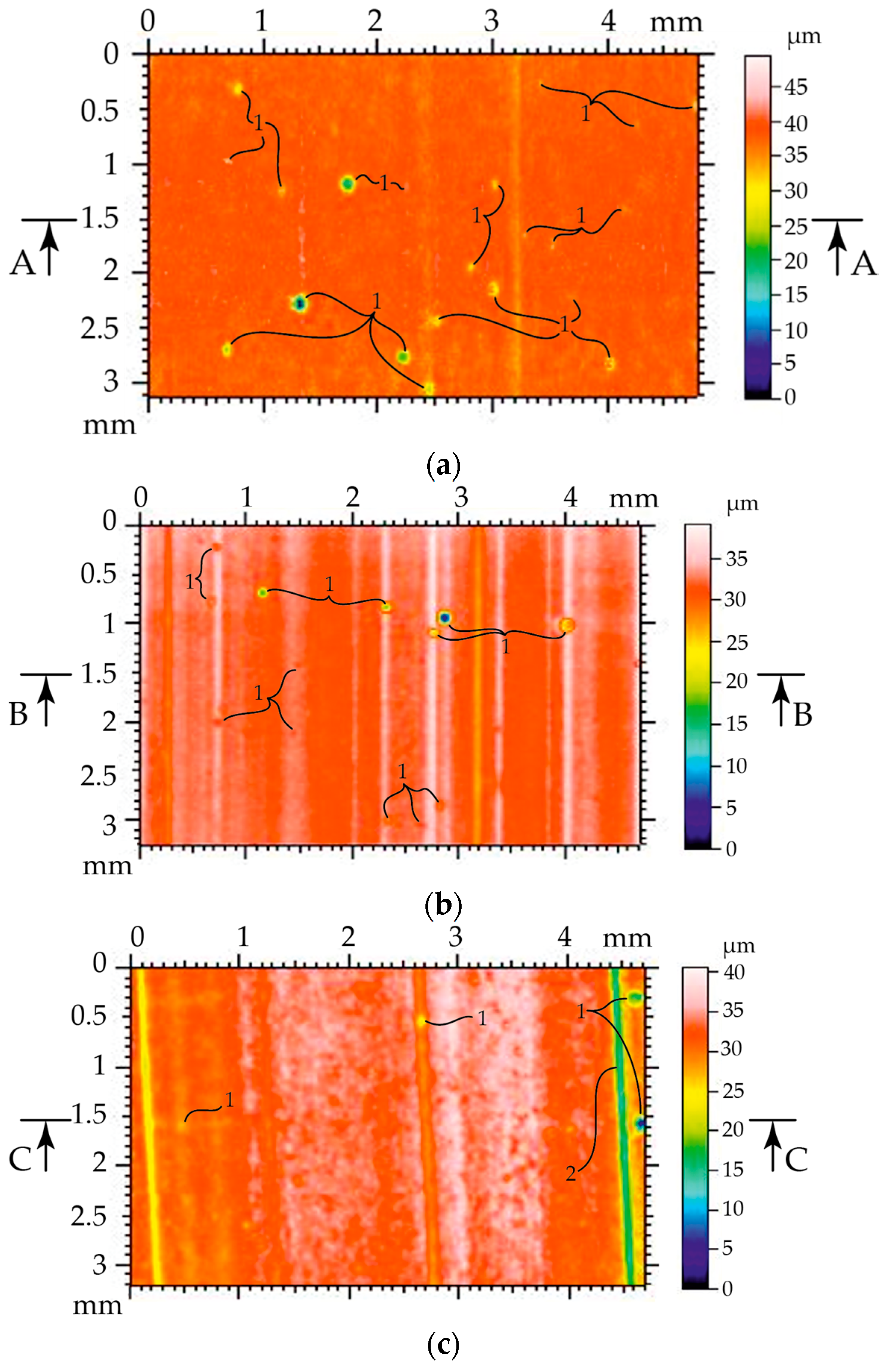
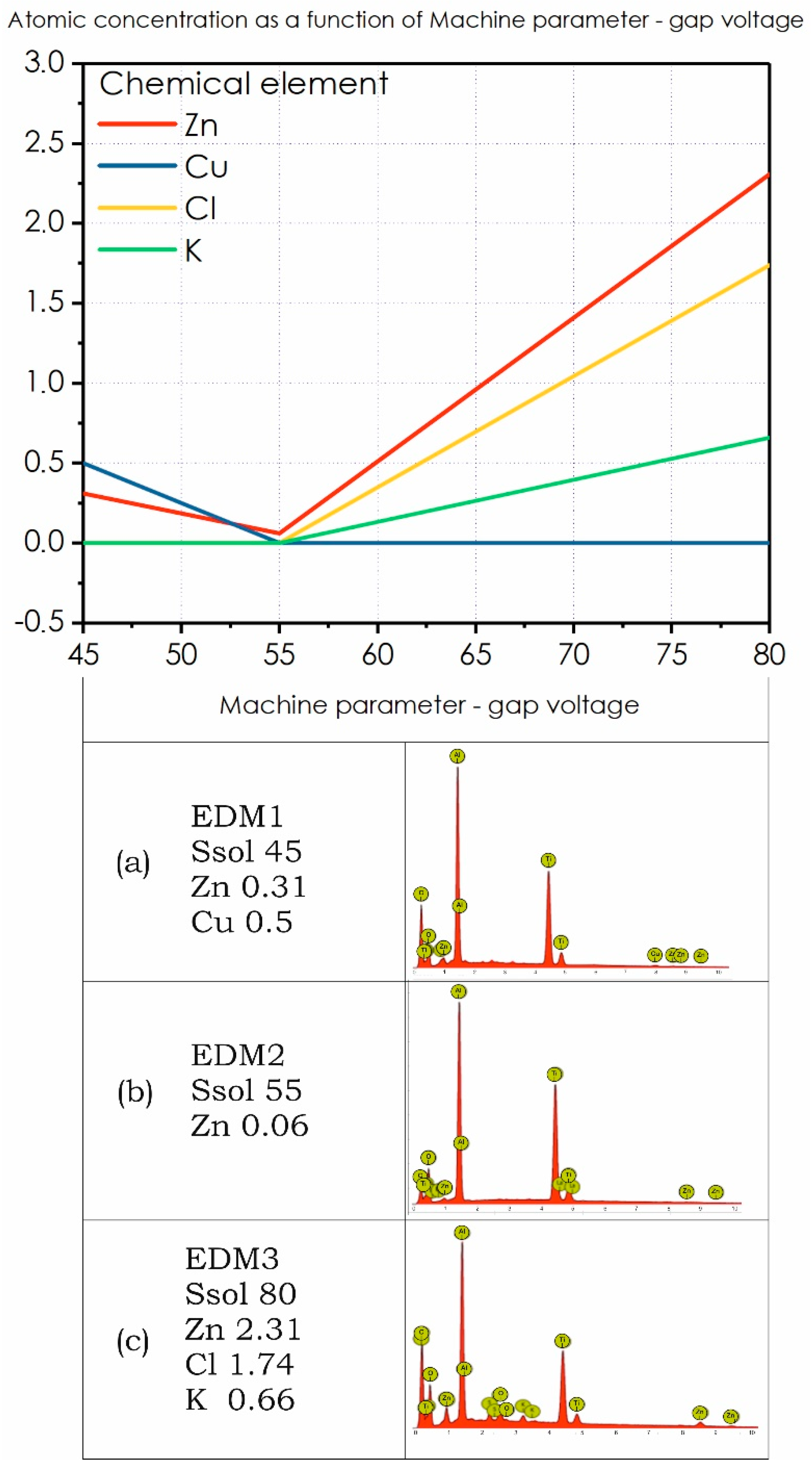
3.2. Chemical Properties of the Surface Layer

The analysis of the quality of the surface layer includes studying contamination of the surface by dielectric and electrode materials. Diffusion in the surface layer adversely affects mechanical properties of workpieces and can significantly reduce the performance of ceramic cutting inserts. Figure 6 shows the change in the structure of workpieces machined using different EDM technologies. As seen in Figure 6, surface porosity decreases with increasing wire speed, which can be explained by a change in the material removal mechanism from melting to evaporation.
Contamination of the surface layer was studied using Phenom ProX via measuring concentrations of dielectric and electrode materials and their products in the surface layer. The measurements show that EDM3 technology featuring the highest discharge energy produces the most contaminated surface, heavily polluted with the dielectric combustion products (Cl 1.74%, K 0.66%) and the wire coating (Zn 2.31%).
This contamination leads to an undesirable increase in the friction coefficient, which adversely affects tool life. EDM1 technology with the smallest SSol and IG is next to EDM3 in terms of the surface contamination, with the primary contaminants coming from diffusion of the wire materials (copper Cu 0.5% and zinc Zn 0.31%) onto the surface being machined. This finding further supports our assumption about the formation of surface defects (in the form of craters) due to insufficient space for flushing out the electroerosion products. In this case, the local breakdown energies were so high that the electric discharge completely melted the protective zinc coating in a fraction of a second, and then the surface was machined with a copper core of the wire. This could occur only in the presence of conductive inclusions—through which an electric current can flow with little resistance—in the IG. EDM2 technology running at higher SSol than EDM1 provided the best purity of surface layer, with contamination being limited to a small amount of the wire electrode coating (Zn 0.06%). In the case, when EDM2 is used, the chemical purity of the surface layer is comparable to that after grinding.

4. Conclusions

In this work, we have explored the possibility of replacing grinding operations with WEDM in manufacturing small-size cutting inserts of a complex shape made of Al2O3–TiC ceramics, identified rational process conditions, and investigated the extent to which WEDM can be used as a grinding replacement. We showed that WEDM, which is a non-contact and, thus, naturally, a more flexible method in terms of the size and complexity of the geometrical parameters of parts being machined, can be used as a replacement for grinding operations when machining small ceramic cutting inserts. We achieved small values of the surface roughness Ra on workpieces made of poorly conductive cutting Al2O3–TiC ceramics using WEDM, which made it possible to use WEDM as a replacement for grinding operations.
Three WEDM regimes with different machine parameter SSol, namely EDM1 (SSol = 45), EDM2 (SSol = 55) and EDM2 (SSol = 80) were used to machine Al2O3–TiC ceramic inserts. Surface roughness values Ra of 0.344 μm, 0.534 μm and 0.907 μm were achieved for EDM1, EDM2 and EDM3, respectively. EDM1 demonstrated the smallest Ra. However, in this case, deep craters were present on the workpiece surface due to too small of a space between the wire and the workpiece, which caused contamination of the working zone. While transfer of the electrode and dielectric materials to the workpiece surface was small, if not negligible, contamination may have reduced the quality of the product surface. Based on the obtained results, we conclude that EDM1 is recommended for use in the machining of reinforcing chamfers (Ra < 0.63 µm) and the front surfaces (Ra < 0.4 µm) of cutting inserts, and may also be used on the rear and support surfaces (Ra ≈ 0.32 µm) of replaceable cutting inserts [49,50].
In cases when EDM3 is used, both the roughness Ra = 0.907 μm and the level of contamination of the surface layer with dielectric and electrode materials were fairly high, and, thus, this technology cannot be recommended for use in the production of cutting inserts.
EDM2 technology, which allows for the achievement of roughness Ra = 0.534 µm and which is the best among the three technologies regarding contamination of the surface layer and defect formation, can be recommended for use in machining reinforcing chamfers (Ra < 0.63 µm) and should be used in a limited fashion for front surfaces (Ra < 0.4 µm) [51,52]. By having all the key processing parameters at the same level when grinding, EDM2 has advantages over EDM1 and EDM3, such the absence of microcraters on the workpiece surface, and also over grinding, such as machining of products of complex shapes with hard-to-reach surfaces, whose curvature is smaller than the curvature of the grinding wheel, and, thus, improved dimensional precession throughout the entire machining cycle.
These considerations lead us to conclude that WEDM is a viable alternative to grinding when machining ceramic cutting inserts of a small size and complex shape, and that its application to manufacturing cutting inserts made of poorly conductive cutting ceramics should be studied further.

Author Contributions

Conceptualization, S.N.G.; methodology, P.M.P., A.B.N.; validation, M.A.V., A.A.Z.; formal analysis, P.M.P., M.A.V., A.A.Z.; investigation, P.M.P., A.B.N.; resources, P.M.P.; data curation, P.M.P., M.A.V.; writing—original draft preparation, A.B.N., P.M.P.; writing—review and editing, S.N.G., A.B.N.; visualization, P.M.P., A.A.Z.; supervision, P.M.P.; project administration, S.N.G. All authors have read and agreed to the published version of the manuscript.

Funding

The study was supported by a grant of the Russian Science Foundation (project No. 21-19-0079).

Acknowledgments

This work was carried out using equipment provided by the Center of Collective Use of MSUT “STANKIN”.

Conflicts of Interest

The authors declare no conflict of interest.

References

  1. Kitagawa, T.; Kubo, A.; Maekawa, K. Temperature and wear of cutting tools in high-speed machining of Inconel 718 and Ti6Al6V2Sn. Wear 1997, 202, 142–148. [Google Scholar] [CrossRef]
  2. Kuzin, V.V.; Grigoriev, S.N.; Fedorov, M.Y. Role of the thermal factor in the wear mechanism of ceramic tools. Part 2: Microlevel. J. Frict. Wear 2015, 36, 40–44. [Google Scholar] [CrossRef]
  3. Grechishnikov, V.; Grigoriev, S.; Pivkin, P.; Volosova, M.; Isaev, A.; Nikitin, D.; Minin, I. Design of toroid-shaped solid ceramic end mill. EPJ Web Conf. 2019, 224, 05001. [Google Scholar] [CrossRef]
  4. Meddour, I.; Yallese, M.A.; Khattabi, R.; Elbah, M.; Boulanouar, L. Investigation and modeling of cutting forces and surface roughness when hard turning of AISI 52100 steel with mixed ceramic tool: Cutting conditions optimization The International. J. Adv. Manuf. Technol. 2015, 77, 1387–1399. [Google Scholar] [CrossRef]
  5. Kuzin, V.V.; Grigor’ev, S.N.; Volosova, M.A. Effect of a tic coating on the stress-strain state of a plate of a high-density nitride ceramic under nonsteady thermoelastic conditions. Refract. Ind. Ceram. 2014, 54, 376–380. [Google Scholar] [CrossRef]
  6. Grigoriev, S.; Peretyagin, P.; Smirnov, A.; Solís, W.; Díaz, L.A.; Fernández, A.; Torrecillas, R. Effect of graphene addition on the mechanical and electrical properties of Al2O3-SiCw ceramics. J. Europ. Ceram. Soc. 2017, 37, 2473–2479. [Google Scholar] [CrossRef]
  7. Volosova, M.; Grigoriev, S.; Kuzin, V. Effect of Titanium Nitride Coating on Stress Structural Inhomogeneity in Oxide-Carbide Ceramic. Part 4. Action of Heat Flow. Refract. Ind. Ceram. 2015, 56, 91–96. [Google Scholar] [CrossRef]
  8. Ghaemi, M.H.; Reichert, S.; Krupa, A.; Zykova, A.; Lobach, K.; Sayenko, S.; Svitlychnyi, Y. Zirconia ceramics with additions of Alumina for advanced tribological and biomedical applications. Ceram. Int. 2017, 4, 9746–9752. [Google Scholar] [CrossRef]
  9. Grigoriev, S.N.; Martinov, G.M. The control platform for decomposition and synthesis of specialized CNC systems. In Proceedings of the Research and Innovation in Manufacturing: Key Enabling Technologies for the Factories of the Future-Proceedings of the 48th CIRP Conference on Manufacturing Systems, Ischia, Italy, 24–26 June 2015; Elsevier: Amsterdam, The Netherlands, 2016; Volume 41, pp. 858–863. [Google Scholar] [CrossRef] [Green Version]
  10. Grigoriev, S.N.; Martinov, G.M. Research and development of a cross-platform CNC kernel for multi-axis machine tool. In Proceedings of the 6th CIRP International Conference on High Performance Cutting, HPC2014, Berkeley, CA, USA, 23–25 June 2014; Elsevier: Amsterdam, The Netherlands, 2014; Volume 14, pp. 517–522. [Google Scholar] [CrossRef] [Green Version]
  11. Liu, J.; Ma, C.; Tu, G.; Long, Y. Cutting performance and wear mechanism of Sialon ceramic cutting inserts with TiCN coating. Sur. Coat. Technol. 2016, 307, 146–150. [Google Scholar] [CrossRef]
  12. Grigoriev, S.N.; Gurin, V.D.; Volosova, M.A.; Cherkasova, N.Y. Development of residual cutting tool life prediction algorithm by processing on CNC machine tool. Mater. Und Werkst. 2013, 44, 790–796. [Google Scholar] [CrossRef]
  13. Ali, A.M.; Abdullah, N.S.; Ratnam, M.M.; Ahmad, Z.A. Linear Shrinkage of the ZTA Ceramic Cutting Inserts. In Proceedings of the 5th International Conference on Recent Advances in Materials, Minerals and Environment (RAMM) & 2nd International Postgraduate Conference on Materials, Mineral and Polymer (MAMIP), Penang, Malaysia, 4–6 August 2015; Elsevier: Amsterdam, The Netherlands, 2016; Volume 19, pp. 879–883. [Google Scholar] [CrossRef] [Green Version]
  14. Grechishnikov, V.A.; Petukhov, Y.E.; Pivkin, P.M.; Isaev, A.V.; Bushuev, S.V.; Romanov, V.B. Prediction and Measurement of the Parameters of the Microtopography of a Surface When Turning Intricately Shaped Parts. Meas. Tech. 2015, 58, 848–853. [Google Scholar] [CrossRef]
  15. Vereschaka, A.; Tabakov, V.; Grigoriev, S.; Aksenenko, A.; Sitnikov, N.; Oganyan, G.; Seleznev, A.; Shevchenko, S. Effect of adhesion and the wear-resistant layer thickness ratio on mechanical and performance properties of ZrN - (Zr, Al, Si) N coatings. Surf. Coat. Technol. 2019, 357, 218–234. [Google Scholar] [CrossRef]
  16. Azhar, A.Z.A.; Mohamad, H.; Ratnam, M.M.; Ahmad, Z.A. The effects of MgO addition on microstructure, mechanical properties and wear performance of zirconia-toughened alumina cutting inserts. J. Alloy. Comp. 2010, 497, 316–320. [Google Scholar] [CrossRef]
  17. Isaev, A.; Grechishnikov, V.; Pivkin, P. Structure and machinability of thin-walled parts made of titanium alloy powder using electron beam melting technology. IOP Conf. Ser. Mater. Sci. Eng. 2016, 123, 012044. [Google Scholar] [CrossRef]
  18. Isaev, A.; Grechishnikov, V.; Pivkin, P.; Kozochkin, M.; Lyuhin, Y.; Vorotnikov, A. Machining of thin-walled parts produced by additive manufacturing technologies. In Proceedings of the Research and Innovation in Manufacturing: Key Enabling Technologies for the Factories of the Future-Proceedings of the 48th CIRP Conference on Manufacturing Systems, Ischia, Italy, 24–26 June 2015; Elsevier: Amsterdam, The Netherlands, 2016; Volume 41, pp. 1023–1026. [Google Scholar] [CrossRef] [Green Version]
  19. Stancekova, D.; Petrů, J.; Svobodová, A. The Application of Grinding of Ceramic Materials. Mater. Sci. Forum. 2018, 919, 215–221. [Google Scholar] [CrossRef]
  20. Zhang, B.; Deng, Z. Grinding of nanostructured ceramic coatings: Surface observations and material removal mechanisms. Int. J. Mach. Tools Manuf. 2002, 42, 1665–1676. [Google Scholar] [CrossRef]
  21. Allor, R.L.; Jahanmir, S. Current problems and future directions for ceramic machining. Am. Soc. Bull. 1996, 75, 40–43. [Google Scholar]
  22. Dražumerič, R.; Badger, J.; Roininen, R.; Krajnik, P. On geometry and kinematics of abrasive processes: The theory of aggressiveness. Int. J. Mach. Tools Manuf. 2020, 154, 103567. [Google Scholar] [CrossRef]
  23. Bilal, A.; Muhammad, J.; Talamona, D.; Perveen, A. Electro-discharge machining of ceramics: A review. Micromachines 2019, 10, 10. [Google Scholar] [CrossRef] [PubMed] [Green Version]
  24. Romoli, L.; Tantussi, G.; Dini, G. Experimental approach to the laser machining of pmma substrates for the fabrication of microfluidic devices. Opt. Lasers Eng. 2011, 49, 419–427. [Google Scholar] [CrossRef]
  25. Vereschaka, A.; Grigoriev, S.; Tabakov, V.; Sotova, E.; Vereschaka, A.; Kulikov, M. Improving the efficiency of the cutting tool made of ceramic when machining hardened steel by applying nano-dispersed multi-layered coatings. Key Eng. Mater. 2014, 581, 68–73. [Google Scholar] [CrossRef]
  26. Tiwari, A.; Mandal, A.; Kumar, K. Multi-objective optimization of electrochemical machining by non-dominated sorting genetic algorithm. Mater. Today Proc. 2015, 2, 2569–2575. [Google Scholar] [CrossRef]
  27. Liu, D.; Cong, W.; Pei, Z.J.; Tang, Y. A cutting force model for rotary ultrasonic machining of brittle materials. Int. J. Mach. Tools Manuf. 2012, 52, 77–84. [Google Scholar] [CrossRef] [Green Version]
  28. Singh, R.P.; Singhal, S. An experimental study on rotary ultrasonic machining of macor ceramic. Proc. Inst. Mech. Eng. Part. B J. Eng. Manuf. 2018, 232, 1221–1234. [Google Scholar] [CrossRef] [Green Version]
  29. Ting, H.; Abou-El-Hossein, K.; Chua, H. Review of micromachining of ceramics by etching. Trans. Nonferrous Met. Soc. China 2009, 19, S1–S16. [Google Scholar] [CrossRef]
  30. Rashid, A.; Bilal, A.; Liu, C.; Jahan, M.P.; Talamona, D.; Perveen, A. Effect of Conductive Coatings on Micro-Electro-Discharge Machinability of Aluminum Nitride Ceramic Using On-Machine-Fabricated Microelectrodes. Materials 2019, 12, 3316. [Google Scholar] [CrossRef] [Green Version]
  31. Tuersley, I.P.; Pashby, I.R.; Jawaid, A. Various methods of machining advanced ceramic materials. J. Mat. Proc. Tech. 1994, 42, 377–390. [Google Scholar] [CrossRef]
  32. Schoth, A.; Forster, R.; Menz, W. Micro wire EDM for high aspect ratio 3D microstructuring of ceramics and metals. Microsys. Tech. 2005, 11, 250–253. [Google Scholar] [CrossRef]
  33. Lauwers, B.; Kruth, J.P.; Liu, W.; Eeraerts, W.; Schacht, B.; Bleys, P. Investigation of material removal mechanisms in EDM of composite ceramic materials. J. Mater. Proc. Tech. 2004, 149, 347–352. [Google Scholar] [CrossRef]
  34. Lei, J.; Wu, X.; Wang, Z.; Xu, B.; Zhu, L.; Wu, W. Electrical discharge machining of micro grooves using laminated disc electrodes made of Cu and Sn foils. J. Mater. Proc. Tech. 2019, 271, 455–462. [Google Scholar] [CrossRef]
  35. Grigoriev, S.N.; Kozochkin, M.P.; Porvatov, A.N.; Marina, A.; Volosova, M.A.; Okunkova, A.A. Electrical discharge machining of ceramic nanocomposites: Sublimation phenomena and adaptive control. Heliyon 2019, 5, e02629. [Google Scholar] [CrossRef] [Green Version]
  36. Smirnov, A.; Kurland, H.D.; Grabow, J.; Müller, F.A.; Bartolomé, J.F. Microstructure, mechanical properties and low temperature degradation resistance of 2Y-TZP ceramic materials derived from nanopowders prepared by laser vaporization. J. Eur. Ceram. Soc. 2015, 35, 2685–2691. [Google Scholar] [CrossRef]
  37. Rashid, A.; Jahan, M.P.; Perveen, A.; Ma, J. Development of trends and methodologies for shaping ceramics by electrical discharge machining: A review. In Proceedings of the ASME 2019 International Mechanical Engineering Congress and Exposition, Salt Lake City, UT, USA, 11–14 November 2019; ASME: New York, NY, USA, 2019; Volume 2A. [Google Scholar] [CrossRef]
  38. Vleugels, J.; Van der Biest, O. Development and characterization of Y2O3 -stabilized ZrO2 (Y-TZP) composites with TiB2, TiN, TiC, and TiC0.5 N0.5. J. Am. Ceram. Soc. 1999, 82, 2717–2720. [Google Scholar] [CrossRef]
  39. Grigoriev, S.N.; Volosova, M.A.; Peretyagin, P.Y.; Seleznev, A.E.; Okunkova, A.A.; Smirnov, A. The Effect of TiC Additive on Mechanical and Electrical Properties of Al2O3 Ceramic. Appl. Sci. 2018, 8, 2385. [Google Scholar] [CrossRef] [Green Version]
  40. Uhlmann, E.; Röhner, M.; Langmack, M. Micro-EDM. In Micro-Manufacturing Engineering and Technology; William Andrew: Norwich, NY, USA, 2010; pp. 39–58. [Google Scholar] [CrossRef]
  41. Puertas-Arbizu, I.; Luis-Perez, C. A revision of the applications of the electrical discharge machining process to the manufacture of conductive ceramics. Rev. Metal. 2002, 38, 358–372. [Google Scholar] [CrossRef] [Green Version]
  42. Mohammad, Y.A.; Maleque, M.A.; Banu, A.; Sabur, A.; Debnath, S. Micro Electro Discharge Machining of Non-Conductive Ceramic. Mat. Sci. Forum 2018, 911, 20–27. [Google Scholar] [CrossRef] [Green Version]
  43. Krebs, G.; Polli, M.L. Cutting parameters for roughing turning of alloy 625 clad using ceramic inserts. Mater. Res. 2019, 22, 20190535. [Google Scholar] [CrossRef] [Green Version]
  44. Bergs, T.; Olivier, M.; Gommeringer, A.; Kern, F.; Klink, A. Surface integrity analysis of ceramics machined by wire edm using different trim cut technologies. In Proceedings of the 5th CIRP Conference on Surface Integrity (CSI 2020), Vitoria-Gasteiz, Spain, 1–5 June 2020; Elsevier: Amsterdam, The Netherlands, 2020; Volume 87, pp. 251–256. [Google Scholar] [CrossRef]
  45. Liu, K.; Reynaerts, D.; Lauwers, B. Influence of the pulse shape on the EDM performance of Si3N4–TiN ceramic composite. CIRP Ann. Manuf. Techn. 2009, 58, 217–220. [Google Scholar] [CrossRef]
  46. Ferreira, J.C. A study of die helical thread cavity surface finish made by Cu-W electrodes with planetary EDM. Int. J. Adv. Manuf. Techn. 2007, 34, 1120–1132. [Google Scholar] [CrossRef]
  47. Smirnov, A.; Seleznev, A.; Solís Pinargote, N.W.; Pristinskiy, Y.; Peretyagin, P.; Bartolomé, J.F. The influence of wire electrical discharge machining cutting parameters on the surface roughness and flexural strength of ZrO2/TiN ceramic nanocomposites obtained by spark plasma sintering. Nanomaterials 2019, 9, 1391. [Google Scholar] [CrossRef] [Green Version]
  48. Grigoriev, S.; Kozochkin, M.; Porvatov, A.; HtuM, T.; Zhavoronsky, P.; Jiang, X.; Pivkin, P. Dynamic model of electrical discharge machining and algorithm of extreme control through acoustic signal. EPJ Web Conf. 2019, 224, 05002. [Google Scholar] [CrossRef]
  49. Grigoriev, S.N.; Volosova, M.A.; Okunkova, A.A.; Fedorov, S.V.; Hamdy, K.; Podrabinnik, P.A.; Pivkin, P.M.; Kozochkin, M.P.; Porvatov, A.N. Electrical Discharge Machining of Oxide Nanocomposite: Nanomodification of Surface and Subsurface Layers. J. Manuf. Mater. Process. 2020, 4, 96. [Google Scholar] [CrossRef]
  50. Trueman, C.S.; Huddleston, J. Material removal by spalling during EDM of ceramics. J. Eur. Ceram. Soc. 2000, 20, 1629–1635. [Google Scholar] [CrossRef]
  51. Grigoriev, S.; Teleshevskii, V. Measurement problems in technological shaping processes. Meas. Tech. 2011, 54, 744–749. [Google Scholar] [CrossRef]
  52. ISO 9361-2, Indexable Inserts for Cutting Tools—Ceramic Inserts with Rounded Corners—Part 2: Dimensions of Inserts with Cylindrical Fixing Hole; International Organization for Standardization: Geneva, Switzerland, 2012.
Figure 1. (a) Cutting insert, its geometry and requirements for Ra. (b) Working zone of the Agie Charmilles CUT 1000 OilTech machine: 1—wire; 2—dielectric oil; 3—device for clamping the workpiece; 4—table.
Metals 11 00882 g001
Figure 2. EDS micrographs depicting chemical composition of the ceramic workpiece measured using Phenom ProX.
Metals 11 00882 g002
Figure 3. Material removal rate (MRR) as a function of machine parameter SSol.
Metals 11 00882 g003
Figure 4. Surface roughness Ra as a function of machine parameter SSol for EDM1 (SSol = 45, Ra 0.344 µm), EDM2 (SSol = 55, Ra 0.534 µm), and EDM3 (SSol = 80, Ra 0.907 µm) measured using the Hommel Tester T8000. 3D images of surface roughness profiles shown in the three lower panels are given for illustration purposes only.
Metals 11 00882 g004
Figure 5. Measurements and graphical representation of the surface roughness carried out using the Hommel Tester T8000: (a)—EDM1; (b)—EDM2; (c)—EDM3; 1—crater; 2—wire breakage.
Metals 11 00882 g005
Figure 6. Atomic concentration of impurities in the surface layer measured using Phenom ProX: (a)—EDM1; (b)—EDM2; (c)—EDM3.
Metals 11 00882 g006
Table 1. Properties of coated copper wire used in the WEDM process. IACS refers to International Annealed Copper Standard. The conductivity in % IACS is calculated based on the conductivity of standard “pure copper” according to IACS.
CoatingConductivity (% IACS)Elongation (%)MaterialTensile Strength (N/mm2)
Zn221.5Brass
CuZn37
900
Publisher’s Note: MDPI stays neutral with regard to jurisdictional claims in published maps and institutional affiliations.

