Article

A Comparison of Methods for the Characterisation of Waste-Printed Circuit Boards

1
Commonwealth Scientific and Industrial Research Organisation (CSIRO) Land and Water, 147 Underwood Avenue, Floreat, WA 6014, Australia
2
Algae R & D Centre, Environmental and Conservation Sciences, College of Science, Health, Engineering and Education, Murdoch University, 90 South Street, Murdoch, WA 6150, Australia
3
College of Science, Health, Engineering and Education, Murdoch University, Murdoch, WA 6150, Australia
4
CSIRO Manufacturing, 36 Gardiner Road, Clayton, VIC 3168, Australia
5
School of Biomedical Sciences, University of Western Australia, Crawley, WA 6009, Australia
6
Faculty of Science and Engineering, School of Mines: Minerals, Energy and Chemical Engineering, Curtin University, Bentley, WA 6845, Australia
*
Author to whom correspondence should be addressed.
Metals 2021, 11(12), 1935; https://doi.org/10.3390/met11121935
Submission received: 12 October 2021 / Revised: 12 November 2021 / Accepted: 26 November 2021 / Published: 30 November 2021
(This article belongs to the Special Issue Processing and Characterization of Metal Containing Wastes)

Abstract

:
Electronic waste is a growing waste stream globally. With 54.6 million tons generated in 2019 worldwide and with an estimated value of USD 57 billion, it is often referred to as an urban mine. Printed circuit boards (PCBs) are a major component of electronic waste and are increasingly considered as a secondary resource for value recovery due to their high precious and base metals content. PCBs are highly heterogeneous and can vary significantly in composition depending on the original function. Currently, there are no standard methods for the characterisation of PCBs that could provide information relevant to value recovery operations. In this study, two pre-treatments, smelting and ashing of PCB samples, were investigated to determine the effect on PCB characterisation. In addition, to determine the effect of particle size and element-specific effects on the characterisation of PCBs, samples were processed using four different analytical methods. These included multi-acid digestion followed by inductively coupled plasma optical emission spectrometry (ICP-OES) analysis, nitric acid digestion followed by X-ray fluorescence (XRF) analysis, multi-acid digestion followed by fusion digestion and analysis using ICP-OES, and microwave-assisted multi-acid digestion followed by ICP-OES analysis. In addition, a mixed-metal standard was created to serve as a reference material to determine the accuracy of the various analytical methods. Smelting and ashing were examined as potential pre-treatments before analytical characterisation. Smelting was found to reduce the accuracy of further analysis due to the volatilisation of some metal species at high temperatures. Ashing was found to be a viable pre-treatment. Of the four analytical methods, microwave-assisted multi-acid digestion offered the most precision and accuracy. It was found that the selection of analytical methods can significantly affect the accuracy of the observed metal content of PCBs, highlighting the need for a standardised method and the use of certified reference material.

1. Introduction

The consumption of electric and electronic equipment (EEE) is growing worldwide. This is fuelled by rapid advancement in technology, increased disposable income, and growing dependence on technology [1]. The production of EEE is estimated to have increased 8% in the year 2018 [2]. When EEE reaches the end of its life and is no longer repairable, it becomes electronic waste (e-waste). E-waste is one of the fastest-growing waste streams globally [2]. In 2019, 53.6 million tons (Mt) of e-waste were generated worldwide. This is expected to increase to 74.7 Mt by the year 2030 [2].
The majority of e-waste globally remains unrecycled or not formally tracked, with only 17.4% formally collected and recycled [2]. Current recycling strategies are not sufficient to support the processing of the increasingly larger amount of e-waste, with an increase of 9.2 Mt of e-waste generated globally per annum since 2014 but only a 1.8 Mt increase in the amount recycled globally per annum since 2014 [2,3]. This is of particular concern in the context of a circular economy. E-waste is comprised of a range of valuable materials that can be recycled, including metals, plastics, and glass [4]. As such, this waste stream is often referred to as an urban mine [5]. The combined total value of all e-waste generated in 2019 was estimated to be USD 57 billion. The most valuable component of e-waste is typically printed circuit boards (PCBs). PCBs only account for 3–6% of the total volume of e-waste globally; however, PCBs are highly valuable due to the high precious and base metals content [1].
In addition to the economic value of e-waste, the environmental impact needs to be considered. The impact of e-waste on the environment can be significant if the waste is not properly managed [6]. PCBs, in particular, contain many hazardous substances, including heavy metals such as lead, mercury, and arsenic, in addition to persistent organic pollutants (POP) and brominated flame retardants (BFR) [6,7]. Improper management of e-waste, e.g., through open burning [8], dust released during mechanical treatment [9], crude recycling processes [10], open disposal [6], as well as illegal dumping [11], can cause air, soil, and water contamination and bioaccumulation of contaminants in the food chain [6,12]. The human health effects of this contamination have also been documented [7]. Therefore, enforcement of proper e-waste management is essential to minimise environmental and health impacts.
Due to their high precious and base metal content, and hence their high value, PCBs are often the focus for e-waste recycling. However, PCBs are generally highly heterogeneous stemming from the diverse functions of the original equipment. PCBs are composed of a mixture of metals (40%), plastics (30%), and ceramics (30%) and can contain over 60 different elements [4,13]. Typically, PCBs are divided into low-grade (<100 ppm Au), medium-grade (100–400 ppm Au), and high-grade (>400 ppm Au) boards [14].
The heterogeneous composition of PCBs makes them a complex material to characterise. Typical PCBs consist of three parts: (1) a non-conducting substrate or laminate usually consisting of plastic or ceramic [15]; (2) a conducting substrate printed on or inside the laminate, which usually consists of highly conductive metals such as copper and gold [15]; and (3) various components such as chips, connectors, and capacitors, which adhere to the surface of the PCBs. [15]. PCBs can be classified as single-sided, double-sided, or multi-layered. The thickness of PCBs can range from 0.2 to 7 mm [15]. The conductive layer can also vary in thickness and typically ranges from 7.5 to 175 μm. The soldering and epoxy can vary significantly depending on the manufacturer, as can the components that are attached to the boards [15]. These components are often closely integrated with resins and epoxy, and discreet separation can be difficult [15]. Given the complexity of the material, it is therefore expected that the composition of PCBs varies significantly depending on the function, the manufacturer, and even the date of manufacturing. The typical composition of metals in PCBs is shown in Table 1. As such, it is critical to extensively characterise the PCBs in order to quantify the composition of the boards accurately. This will allow the quantification of metal flows in metal extraction processes, calculating any loss in metals and the extraction yields. This is essential to evaluate the efficiency of metal extraction processes and their potential for large-scale implementation.
Although a notable number of studies on PCBs have been conducted (Table 2), there is no set standard for the accurate characterisation of the material. Different methodologies have been investigated for characterising metals composition in PCB waste, with the majority relying on acid digestion to solubilise the metals present (Table 2). Noteworthily, little research has been conducted to determine the optimal method for e-waste characterisation [16,17,18,19,20,21]. Even fewer studies have attempted to create a reference material (RM) to determine the accuracy of the employed analytical methods [19,22]. Often the method with the highest yield is considered the best, but this does not consider the precision of the methods [16,18]. Therefore, this study compared the precision of a variety of analytical methods (AM) for characterising the metal content of PCB samples. The study also evaluated ashing and smelting as possible pre-treatments prior to acid digestion (Figure 1). In addition, a mixed-metal standard (MMS) was used to investigate the accuracy of the methods used.

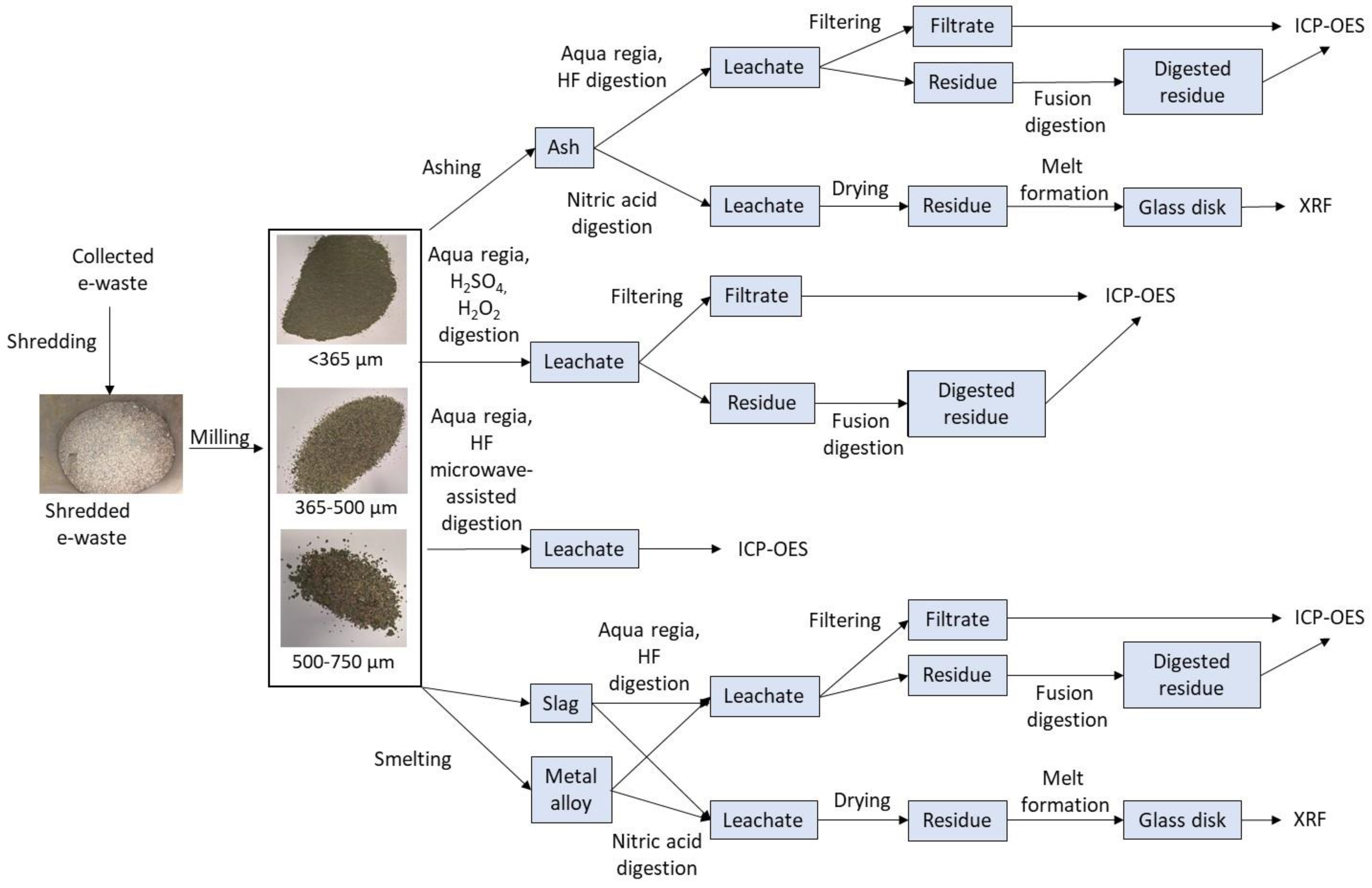
2. Materials and Methods

2.1. Printed Circuit Board Preparation

Shredded (2 cm) high-grade PCBs removed from electronic equipment were supplied by MRI e-cycle solutions. The PCBs were ground using a LM1-M ring mill (LabTechnics Australia, Victoria, Australia) and sieved to three size fractions: <365 μm, 365–500 μm, and 500–750 μm using a Retch AS200 control sieve shaker. Each size fraction was weighed to determine the relative mass of each size fraction. Each size fraction was then individually subsampled using a RSD.30L.12.13/8751 rotary sample divider (Wallerby Mining Products, New South wales, Australia) to obtain representative samples for elemental analysis.

2.2. Mixed-Metal Standards (MMS)

Mixed-metal standards were created using analytical-grade elemental metal powders. The following chemicals were sourced from Sigma Aldrich: iron 12310-500G-R, copper 266086-500G, zinc 324930 10G, nickel 266981-500G, tin 14509-250G-R, and aluminium 653608. These powders were weighed using an analytical balance, and the weights were recorded to three decimal places before mixing the metal powders into composite samples and submitting for analysis.

2.3. Analytical Methods

Three replicate samples of each PCB size fraction were subjected to each of the analytical methods used for determining element contents (Table 3). The total elemental content for the entire batch of PCBs was calculated using the Equations (1) and (2) considering the total mass of each size fraction:
TMelement = (Mf1 × C1/100) + (Mf2 × C2/100) + (Mf3 × C3/100)
TCelement = TMelement/TMtotal
where TMelement is the total mass (kg) of the element for all particle sizes; Mf1, Mf2, and Mf3 are the masses (kg) of size fractions 1 (<365 μm), 2 (365–500 μm), and 3 (500–750 μm), respectively; and C1, C2, and C3 are the contents (%) of the element in size fractions 1, 2, and 3, respectively. TC is the total content (%) for the element for the batch of PCBs processed. TMtotal is the total mass (kg) of the batch of PCBs processed.

2.3.1. Ashing

Ashing of the milled PCB waste was conducted in open ceramic dishes, in air, in a Modutemp SC1268 VMO muffle furnace. Samples of 2.5–3 g of PCBs or 3.37 g of MMS were slowly heated to 500 °C and held at 500 °C for 4 h before slowly cooling to ambient temperature for weighing. Ashed material was slightly “sintered” post ashing and was broken up using a mortar and pestle before sub-sampling for chemical analysis. The loss on ignition (LOI) was calculated using Equation (3):
LOI = (msample − mashed) × 100%/msample
where msample is the sample mass (g) before ashing, and mashed is the sample mass (g) after ashing. The element content in the original sample (Coriginal sample) was calculated using Equation (4):
Coriginal sample = Celement ashed × (100 − LOI)/100
where Celement ashed is the content of the element (%) in the ashed sample as determined by X-ray fluorescence (XRF) or inductively coupled plasma optical emission spectrometry (ICP-OES) analysis. MMS samples were processed using the same method.

2.3.2. Smelting

Smelting of the milled PCB samples was conducted in a Modu-Temp SC1268 VMO muffle furnace. Samples of 50 g of milled PCBs or 54.04 g of MMS were fused with 50 g of borax (Gitz Green, batch ID: 1116010C) (Na2[B4O5(OH)4]·8H2O) in alumina (for e-waste) or graphite (for mixed-metal standards) crucibles using a muffle furnace at 1350 °C for 3 h. A graphite crucible was used for MMS because alumina crucibles melted in the first PCB sample smelting trial due to overheating. The metal phase was separated from the slag by screening at 106 µm either directly to produce metallic prills or by re-melting the coarse >106 µm fraction to produce a metallic button. The metal (>106 µm) and slag (<106 µm) phases were then weighed, with the metal phase forming 44.89–75.3% of the total mass and the slag phase forming 55.10–24.67% of the total mass, depending on the fraction size. Each phase was analysed separately for elemental composition. The contents of each phase and the masses of the recovered phases were used to calculate the metal content of the original PCB samples. The element content for the original sample (Coriginal sample) was calculated using Equations (5)–(8):
m1 = (mmetal phase recovered × C1)/100
m2 = (mslag phase recovered × C2)/100
melement total = m1 + m2
Coriginal sample = (melement total × 100)/msample
where m1 and m2 are the masses (g) of the element in the metal phase and the slag phase, respectively; mmetal phase recovered and mslag phase recovered are the masses (g) of the metal and slag the phases recovered from smelting, respectively; C1 and C2 are the contents (%) of the element in the metal phase and the slag phase, respectively, as determined by XRF or ICP-OES; melement total is the total mass (g) of the element in the sample; and msample is the mass (g) of the sample used for smelting. MMS samples were processed using the same method. The LOI for smelting was calculated using Equations (9) and (10):
minput = msample + (mborax × 0.528)
LOI = (minput − msmelted) × 100/minput
where minput is the total mass (g) submitted for smelting; msample is the mass (g) of the PCB sample submitted; mborax is the mass (g) of the borax added to the PCB sample; and msmelted is the mass (g) of the sample recorded after smelting. The mass of the borax was multiplied by 0.528 to account for the loss of water from the mass of borax (Na2[B4O5(OH)4]·8H2O) during the smelting process.

2.3.3. Analytical Method 1: (AM1) X-ray Fluorescence (XRF) for Ashed and Smelted Samples

Subsamples of ashed PCB and MMS residues (0.2–0.3 g) or smelted PCB and MMS phases (0.4–0.5 g for slag phases and 0.1–0.15 g for metal phases) were treated with ~5 mL of concentrated nitric acid and 1 mL of Milli-Q water in a water bath at 100 °C with sonication (35 kHz, Transsonic 780/H, Germany) of 2–3 bursts of 15 min to ensure mixing for 1–2 h until no reaction could be observed (effervescence). The reacted material was transferred to Pt-ware and dried at 80 °C on a hot plate. Thereafter, 5 g at a 12:22 mass ratio of lithium-tetraborate-to-lithium-metaborate flux was added to the dried material in a crucible and fused by heating at ~1000 °C, swirling over an oxy-propane burner until a homogenous melt was achieved. The melt was poured into a heated Pt mould and then cooled to make a 30 mm glass disk for X-ray fluorescence (XRF). The XRF analysis was conducted using a Bruker S8 Tiger 4 kW WD-XRF to determine the metal content of the sample.

2.3.4. Analytical Method 2 (AM2): Inductively Coupled Plasma (ICP) Optical Emission Spectrometry (OES) for Ashed and Smelted Samples

Subsamples of the ashed PCB and MMS residues or smelted PCB and MMS phases (0.1 g) were weighed with an analytical balance and digested in Teflon beakers with aqua-regia made from 2 mL of concentrated nitric acid, 6 mL of concentrated hydrochloric acid, and 10 mL of 48% hydrofluoric acid at 200 °C for several hours to fume off the hydrofluoric acid. After taking to near dryness, the solutions were diluted to 100 mL volume using 5% nitric acid. Where required, all samples were filtered (Millipore 0.45 µm HVLP polyvinylidene fluoride membrane filters) to collect any undigested sample or residue that was formed. The filtrate solutions were diluted appropriately for analysis by Agilent 730 ICP-OES for elements of interest. The residues were fused in 1 g of lithium borate flux with a 12:22 mass ratio of lithium tetraborate to lithium metaborate by heating at ~1000 °C and swirling over an oxy-propane burner until a homogenous melt was achieved. The melt was then cooled before digestion in a Pyrex beaker in 5 mL of concentrated (37%) hydrochloric acid and 80 mL of Milli-Q. The solution volume was adjusted to 100 mL with Milli-Q for analysis by ICP-OES on an Agilent 730 ICP-OES. Lithium borate matrix-matched calibration standards were used for the analysis of minor elements by ICP-OES. The metal contents from the filtrates and digests of the fused residues were combined to determine the metal content of the sample.

2.3.5. Analytical Method 3 (AM3): Piranha, Aqua Regia Digestion and Direct Fusion Digestion Followed by ICP-OES

PCB and MMS subsamples were digested in a piranha solution made with 30 mL of 98% sulfuric acid and 10 mL of 30% hydrogen peroxide for 1 h at 100 °C while being stirred using a magnetic stir bar. After 1 h, aqua regia made with 35 mL of concentrated HCl and 15 mL of concentrated HNO3 was added, and samples were digested for another hour at 100 °C. Following this, samples were filtered using 0.1 μm Isopore polycarbonate filters. The resulting filtrate was diluted to 250 mL using ultrapure water. The filters were placed in a platinum crucible and placed in a furnace at 1000 °C for 10 min to ash the filters. Following this, 3 g of sodium tetraborate flux was added, and samples were further digested in the furnace at 1000 °C for 1 h. The whole crucibles were placed in 75 mL of 5% nitric acid and shaken overnight to solubilise the samples. This solution was diluted to 100 mL with ultrapure water. Both the acid digest solution and the fusion digest solution were diluted to 1:10 using 0.2% nitric acid and were analysed using a Thermo Scientific ICAP 7600 Duo ICP-OES. The elemental content of the original sample (Coriginal sample) was calculated using Equations (11)–(14):
m1 = C1 × V1 × D1
m2 = C2 × V2 × D2
mtotal = m1 + m2
Coriginal sample = (mtotal × 100)/msample
where m1 and m2 are the total masses (g) of the element from acid digestion and fusion digestion, respectively; C1 and C2 are the content (%) of the element measured for the acid digest and the fusion digest, respectively; V1 and V2 are the volumes (mL) to which the acid digest and fusion digest solutions were diluted, respectively; D1 and D2 were the dilution factors for the acid digest and the fusion digest, respectively; and mtotal is the total mass (g) of the element in the sample.

2.3.6. Analytical Method 4 (AM4): High-Temperature and -Pressure Acid Digestion Followed by ICP-OES

PCB subsamples were digested using 1 mL of 48% HF, 5 mL of 36% HCl, and 2 mL of 70% HNO3 in an Anton Parr MW3000 microwave digestion system at a temperature of 180 °C and at 30 bar pressure for 20 min. Following the digestion, samples were diluted and analysed using a Perkin Elmer Optima 7300DV ICP-OES. MMS samples were analysed using the same method without any subsampling.

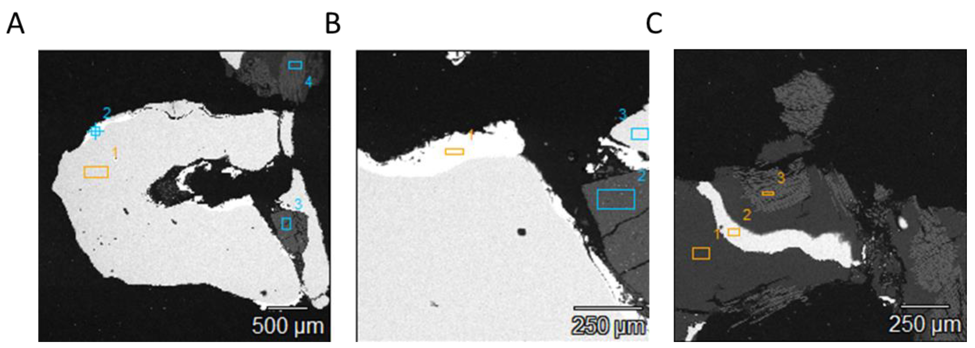
2.3.7. Scanning Electron Microscopy (SEM) Energy Dispersive Spectrometry (EDS) Analysis of PCB Particles

SEM-EDS was conducted by AXT, Australia, on a subsample of the smallest PCB size fraction. The sample was mixed with graphite before being set in a resin block and polished using a semi-automated system, Hexamatic by Struers. The resin block was prepared using EpoFix resin from Struers and was analysed using a Vega3 Tescan.

2.4. Statistical Analysis

The statistical significances of the results were determined using analysis of variance (ANOVA) with replication with differences considered significant at p values <0.05. All statistical analyses were conducted on Microsoft Excel using the Analytical Tool Pack. The relative standard deviation (RSD) for the individual elements was calculated using Equation (15):
RSDelement = (SDelement × 100)/averageelement
where RSDelement is the RSD is the specific element; SDelement is the standard deviation of the individual element; and averageelement is the average content for the element across the three replicates.

3. Result and Discussion

The elemental content of three particle size fractions of PCBs as determined using various AMs is shown in Figure 2 and Table 3. Each of the three fractions was tested in triplicate to determine the variability of the results. In doing so, it was possible to determine the effect particle size has on detected metal content as well as the advantages and limitations of the different processing methods.

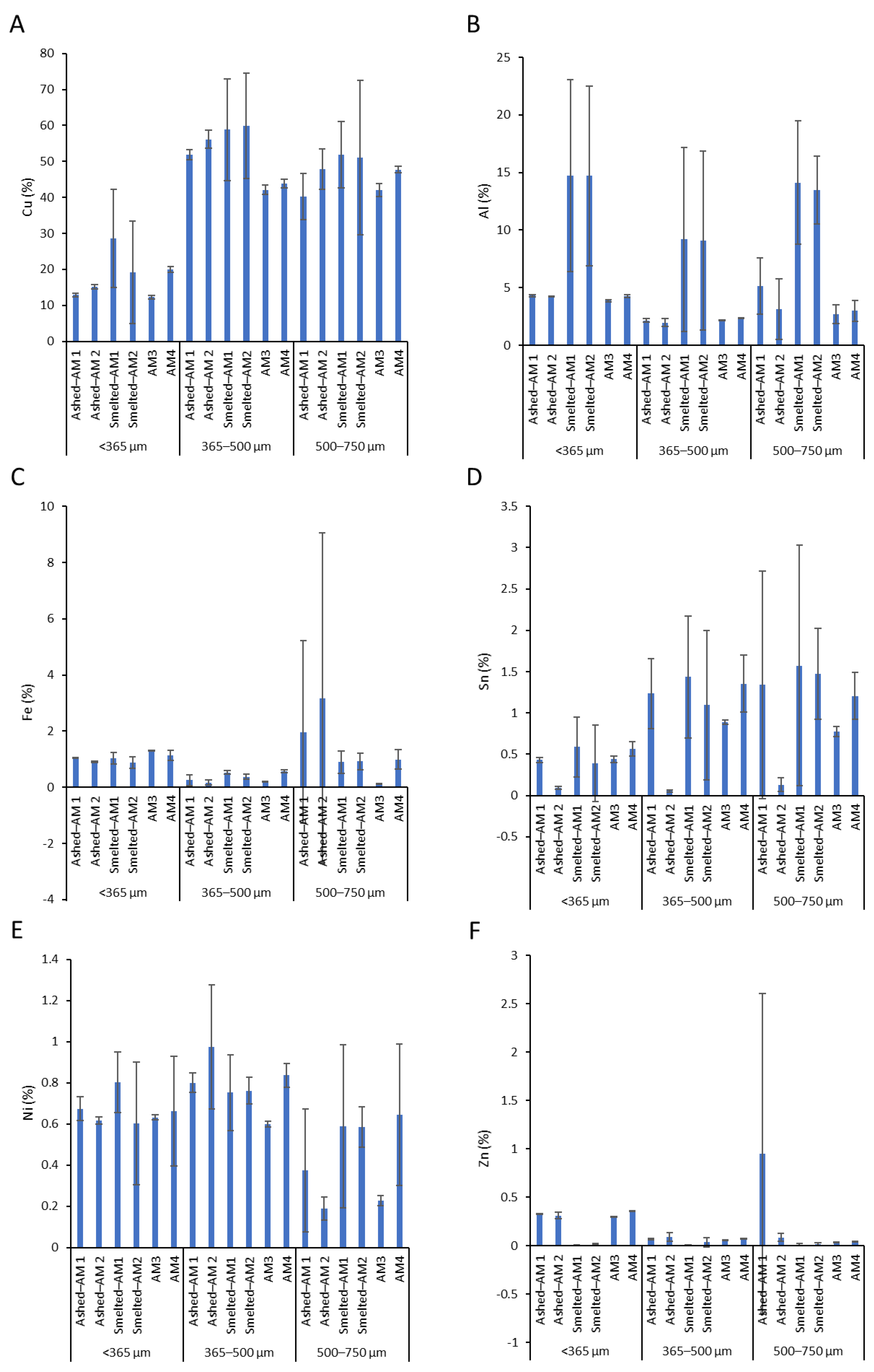
3.1. Metal Content of PCB Samples

The content of Cu, Al, Fe, Sn, Ni, and Zn in the PCB samples as analysed with various methods are shown in Figure 2. In general, Cu was the dominant metal in the PCBs, with content varying from 12.18 to 58.93% depending on the particle size and the method used. The contents of Al, Fe, Sn, Ni, and Zn in the various particle sizes varied in the ranges of 1.97–14.1%, 0.13–3.17%, 0.05–1.57%, 0.22–0.97%, and 0.005–0.94%, respectively, depending on the methods used (Figure 2).

3.2. Effect of Particle Size on Metal Content

To determine the effect of particle size on the detected metal content, three different size fractions were selected and characterised using all four AMs (Figure 2). Significant variation (p < 0.05) was found between size fractions for all metals except for magnesium and sodium. Analysis of smelted PCB phases with AM1 and AM2 showed high magnesium and sodium contents throughout all three particle sizes, and no significant variation (p > 0.05) was detected between different particle sizes. No other analytical methods showed notable magnesium or sodium contents.
In this study, RSD was determined to evaluate the variability of the metal contents between size fractions. Generally, the <365 μm fraction had the lowest RSD, and the RSD increased with increasing particle size (Figure 3). This was consistent with Gy’s theory of sampling, in which smaller sized fractions are more homogenous compared to large-size fractions of equivalent mass and hence are more representative of the original material [49]. There are numerous factors that contribute to this reduced variability. The reduced particle size and increased sample mass will increase the likelihood of selecting a homogenous sample. In addition, by reducing the particle size and increasing the surface-to-volume ratio, the metals are more likely to be exposed to leaching agents, thereby increasing the efficiency of metals leaching, or dissolution from the PCB particles is solubilised. Touze (2020) investigated the relationship between particle size and sample mass to measure the metal content in PCBs and showed that the same principle applies to PCBs [50]. They found that the largest sample mass (5 g) and the lowest particle size (200 μm) resulted in the lowest variability in the samples. This variability significantly (p < 0.05) increased as particle size increased and sample size decreased. However, in the present study, metal contents detected after smelting deviated from this trend. For smelted PCB samples, the smallest particle size demonstrated a large RSD for both AM1 and AM2. This was contradictory to Gy’s sampling theory, given that smelting also used the largest sampling mass (50 g), and the high-temperature processing should reduce the encapsulation of metals with plastics that are combusted during the process [51]. However, as discussed later, there are other chemical processes that can affect the accuracy and precision of the methods.
For other AM, there were specific metals that had a high RSD in the smaller particle sizes (Figure 3). Typically, these metals were Sn and Ni. This is likely due to the heterogeneous composition of PCBs and the unique physical properties of the material. PCBs typically consist of different layers of plastic, metal, and fibre-glass-enforced resin with various components soldered onto the top layer. This results in a highly variable and diverse composition with up to 60 different elements, both pure elements as well as alloys, in unique combinations. Due to the spatial positioning and concentration of these metals, as well as the physical properties, lumps of pure metal can exist even after extensive size reduction. These “nuggets” reduce the homogeneity of the sample and can result in larger RSD even in a considerably small sized fraction.
One method to achieve a more homogeneous sample is to further reduce the particle size of the material. However, PCBs have a limit on how effectively size reduction can occur. The smallest size that PCBs can typically be reduced to without extensive treatment is 250 μm [50]. This is largely due to the physical properties of the particles, with plastics being more brittle and metals typically being more ductile and malleable. The plastic content also typically increases with the reduction in the size of the fragment, as observed in this study (Figure 4). Smelting and ashing allowed the calculation of organic material content through loss on ignition (LOI) as the organic components were combusted. The largest LOI was detected in the smallest particle sizes (Figure 4).

3.3. Effect of PCB Sample Pre-Processing

3.3.1. Smelting

E-waste samples were fused with borax in alumina crucibles in a muffle furnace at 1350 °C. Following smelting, the metal phase was separated from slag, and both phases were subsampled for both XRF (AM1) and ICP-OES (AM2) analysis. Sample pre-processing using smelting was chosen as it allowed for a larger sample size (50 g) and the removal of any combustible organic substances such as BFR and plastics during the high-temperature processing. The resulting ceramics and metals were separated after the smelting process by screening the sample based on size. This was done to simplify the acid digestion step by reducing the amount of metal bound to ceramics, plastics, and silicates [16].
In accordance with Gy’s theory of sampling, the larger sample size should reduce the variability in the results [52]. Typical PCB characterisation processes have used 0.1–3 g PCBs (Table 1), which, depending on the particle size, could still not be representative [52,53]. However, surprisingly, the smelting processes provided the largest variation in metal content among all the methods investigated (Figure 3).
Specific metals showed significant variation (p < 0.05) in metal content after smelting as compared to other methods used. These included copper, zinc, aluminium, tin, sodium, and magnesium. The zinc content for samples analysed using smelting showed significantly (p < 0.05) lower content compared to other processing methods (Figure 2). This was due to the vaporisation of zinc during the smelting process. When temperatures exceeded 920 °C in atmospheric pressure, the carbon present in PCBs can be oxidised to form CO (reaction 16), which in turn reacts with zinc oxide to generate volatile zinc that can be lost as a gas (reaction 17) [54]:
2C +O2(g) → 2CO(g) + heat
(ZnO) +CO(g) → Zn(g) + CO2(g)
At an industrial scale, this occurs during the black copper smelting process, which can be adapted to recycle and extract precious metals from PCBs [55]. The volatilised zinc can then be recovered by capturing the gas and condensing it in a baghouse filter [55]. To ensure a more accurate determination of zinc content in PCBs using smelting, it is advisable that the fumes from the furnace be collected in the baghouse filter and analysed using ICP-OES [56].
The content of aluminium and sodium in the PCB samples appeared significantly (p < 0.05) higher when processed using smelting as compared to other methods. The apparent sodium content was 12.16%, 8.80%, and 10.34% for the particle sizes <365 μm, 365–500 μm, and >750 μm, respectively, when analysed using AM1 after smelting and 11.16%. 8.47%, and 9.74 % for the particle sizes <365 μm, 365–500 μm, and >750 μm, respectively, when analysed using AM2 after smelting. There was no significant difference (p > 0.05) between particle sizes or between AM1 and AM2 used for the smelted samples. The high sodium content detected after smelting was partially due to the use of borax (sodium borate) and represented a large percentage of the total mass present in smelted phases. Even when factoring in the mass of sodium present in the borax, the detected sodium content was still significantly higher (p < 0.05). As such, smelting with borax is not appropriate to determine the sodium content in PCB samples. Since sodium is not commonly tested for PCBs, this is not likely to be a major concern.
The increased aluminium content can be attributed to the use of alumina crucibles. Alumina crucibles are composed of Al2O2 [57]. These crucibles are rated for use up to 1500 °C [57,58]. However, they are not considered optimal when determining the aluminium content in samples [56,58]. The crucibles lost weight during the smelting process, indicating that some of the crucible material may have dissolved into the samples, which could increase the detected content of aluminium in the samples. An alternative would be to use graphite or porcelain crucibles for smelting [56,58]. These crucibles are still stable at high temperatures and will not become solubilised during the smelting process [58].
The magnesium content of the smelted samples (7.18–10.33%) was significantly higher (p < 0.05) compared to other methods (data not shown). Magnesium is not a common component in PCBs, as was observed across other methods used, which showed a percentage content of Mg ranging 0.03–0.28%. A similar range has also been previously reported for other methods [50] However, after smelting, the magnesium content was 7.88%, 10.33%, and 7.18% for the <365 μm, 365–500 μm, and 500–750 μm fractions, respectively, when analysed using smelted AM1 (Supplementary Figure S1). There was no significant difference (p > 0.05) in the Mg between particle sizes of smelted PCB phases analysed with AM1 and AM2. Some material used for fusion digestion can contain trace amounts of magnesium, and the influence of this on the final composition is usually accounted for by testing blank samples, which contain fuse material without the sample. However, for this AM, the borax used was 99.9% pure; therefore, the magnesium that may be present as an impurity in borax cannot explain the high Mg content detected in the samples. Hence, it is not known why the large magnesium content was recorded in the smelted samples.
Smelting PCB samples resulted in the highest copper content for both AM1 and AM2 compared to all other AMs. However, smelting also had the largest RSD for copper. This large variation in metal content in samples from smelting can be a result of the non-metallic composition of PCBs. One common component of PCBs is BFR [59]. BFR are used to inhibit combustion reactions and reduce the flammability of PCBs [60]. The most commonly used BFR is tetrabromobisphenol A (TBBPA) [60]. It is used in over 70% of all electronic and electrical equipment worldwide [61]. The rapid decomposing of TBBPA during thermal processing has been well characterised [59,62,63]. During the thermal decomposition of TBBPA, a range of phenol-based products are formed, but the most common product is HBr [61]. Although the decomposition of TBBPA starts at 180 °C, it is not significant when the temperature is below 270 °C [63]. However, when the temperature is increased to 320 °C, over 90% of TBBPA are decomposed, with full decomposition occurring at 500 °C [61].
This is of particular importance in high-temperature processing for PCB characterisation because the resulting HBr from TBBPA decomposition reacts with metal species according to reaction 18 [61]:
4M(s,l) + 4HBr(g) → 4MBr(s,l) + 2H2
where M is the metal species present in PCBs. The resulting MBr is rapidly volatilised at high temperatures according to reaction 19 [61]:
MBr(s,l) → MBr(g)
This reaction can have significant effects on the detected metal content of PCBs. Oleszek (2013) documented the reactions of HBr with copper, silver, and gold [61]. When HBr was in excess, up to 50% of copper and silver were lost due to the volatilisation of MBr at temperatures of 600–1000 °C [61]. Gold was documented to be resistant to HBr, and no mass was lost in the samples. This mobilisation of copper and silver, when reacted with HBr, would contribute to the large RSD detected for smelted samples, despite a large initial sample mass. Currently, the formation of other metal bromide species (MBr) is not well characterised, and hence more research is warranted. To increase the accuracy of PCB characterisation with smelting, it is necessary to recover the fumes in a baghouse filter [56] or collect the condensation of MBr using quartz wool as described in Oleszek (2013) [61].
The possible loss of some metals upon reacting with HBr may account for the large RSD value of the smallest-sized fraction processed using smelting (Figure 3). The plastic content of the smallest-sized fraction was larger compared to the other-size fractions (Figure 4). Since it is the plastics in PCBs that contain the majority of BFR, the concentration of BFR would likely be largest in the smallest-sized fraction [61]. This would increase the presence of HBr during smelting, which would react with the metals present in the sample at the temperatures used.
Despite the large sample mass used and the combustion of plastics prior to elemental analysis, there was still significant variation in the metal content of the smelted samples. Contributing to this variability was the volatilisation of zinc as well as the mobilisation of metals due to the formation of HBr from BFR. The smelted samples analysed with AM1 and AM2 had the largest RSDs of any of the methods used and, as such, the lowest precision. The precision could be improved by collecting any volatilised metals in a baghouse filter for subsequent analysis using ICP-OES [56] as well as by conducting the process at a temperature below 900 °C to prevent the volatilisation of zinc [54]. This could make smelting a more viable method to characterise PCBs.

3.3.2. Ashing

Ashing is an alternative means of sample pre-treatment accomplished by heating the sample in a crucible at standard atmospheric conditions [64]. This is typically done in an enclosed muffle furnace and results in the evaporation of volatile material, the oxidation of non-volatile residue, and the combustion of organic matter [65]. Ashing can be followed with acid digestion to solubilise any residue before characterisation.
Ashing was chosen as an alternative high-temperature processing method to smelting to characterise PCB samples. Ashing was done at a lower temperature, 500 °C, without the addition of borax to combust any organics in the sample. The most common plastics in PCBs are acrylonitrile-butadiene-styrene (ABS) and high-impact polystyrene (HIPS) [66]. These plastics have boiling points of 145.2 °C and 430 °C, respectively [67]. At the ashing temperature of 500 °C, all plastics should be combusted. In addition, at 500 °C, TBBPA will have fully decomposed, forming HBr [61]. However, unlike the temperature at which smelting was conducted, the formation of MBr should be minimal, as a notable formation only occurs at temperatures above 600 °C [61]. As such, ashing may allow the decomposition of pollutants and the combustion of plastics without the associated loss of metals.
In this study, ashing was followed with acid digestion to solubilise any remaining material. Any residue that remained from the acid digestion was filtered and fused. When compared to other methods, with the exception of those pretreated with smelting, a significant difference (p < 0.05) in copper and tin content was detected after ashing (Figure 2). After ashing, an insoluble iron and copper residue was seen in crucibles. This residue sample was resuspended using 5% nitric acid and analysed using ICP-OES. The masses of these residues were minimal, representing between 0.02 to 0.25% of the total sample mass, which would have minimal effect on the final content analysis. The RSD of copper in the ashed samples was also relatively low in the smallest-sized fraction at 3.9%. This increased to a larger 11.7% in the largest-sized fraction (Figure 3). This variation could be a result of the heterogeneous composition of PCBs. When samples were analysed using SEM-EDS, distinct nuggets of copper and tin were detected despite the grinding of the samples for the preparation of the sample to form the resin block for SEM analysis (Figure 5) (Table 4). A similar observation was reported by researchers, who recorded large RSD for nickel (10%) and zinc (35%) even when using a sample mass of 5 g and 16 replicates [50]. This was attributed to the nugget effect of these metals. A comparable effect was observed for iron and cobalt in previous work [50]. Despite the large RSD for iron and nickel in the present study, no significant differences were found between AMs for these elements. When the particle size was reduced, the RSD notably decreased as well (Figure 2).
There was a significant variation (p < 0.05) in the detected tin content of PCBs between AM1 after ashing and the other AMs. The tin content for AM2 after ashing was consistently low across all particle sizes. When processed by ashing, tin had a large RSD in even the <365 μm fraction at a content of 12.27% when analysed using AM2 after ashing (Figure 3). The RSD increased to 62% for the 500–750 μm fraction (Figure 3). The low tin content was not observed in AM1 after ashing, which had a higher tin content than AM2. No significant variation (p > 0.05) was observed between AM1 after ashing and AM3 or AM4 for tin. Complete digestion and solubilisation should have occurred using AM2 for ashed samples [68]. There have been reports of metals not solubilising during the wet digestion process if large amounts of silicates are present [69]. However, the use of HF acid is typically sufficient to digest any silicates and prevent this from occurring [69]. It is possible that the sample was still heterogenous after ashing, considering that the SEM-EDS results showed that distinct nuggets of tin were present in the sample after grinding with no further pre-treatment (Figure 5). Additional steps to homogenise the sample after ashing might need to be taken in addition to increasing the sample mass for digestion [50].
Based on the literature, the ashing of samples at 500 °C prior to acid digestion can remove BFR without causing the volatilisation of metals [61]. The temperature at which ashing occurred was sufficient to combust the most-common plastics found within PCBs [67]. The encapsulation of plastics by metals has been shown to affect the solubilisation of metals in acid [16]. After pretreating PCBs by ashing, subsequent acid digestion would be more effective and could help reduce the variability in sample characterisation. This was reflected in the low RSDs for most of the base metals examined (Figure 3), when compared to smelting. Based on these results, ashing can be advantageous as a pre-treatment in characterising PCBs.

3.4. ICP-OES vs. XRF Analysis for Ashed and Smelted Samples

After ashing and smelting, subsamples were digested and then analysed using both XRF (AM1) and ICP-OES (AM2). The analysis of PCB samples by acid digestion followed by ICP-OES analysis is common (Table 2). As well as being common, the analysis of ashed PCBs using XRF has also been shown to be precise [70]. However, due to heterogeneity, PCBs are a difficult material to characterise precisely. As such, both ICP-OES and XRF were used to determine if the results were comparable and to identify any limitations in the techniques.
Before analysis using any technique, a bulk substance must be homogenised and riffled to enable a representative sub-sample, and this is challenging for PCBs. The sample size for ICP-OES analysis is typically 100 mg [71], so if the sample is not completely homogenous or representative of the bulk, the results will be variable. For accurate analysis by ICP-OES, the representative subsample must be fully digested, without loss or contamination, to produce a clear solution with the elements of interest. These elements must be stable and remain solubilised long enough for analysis to be completed. To avoid contamination of the sample, the digestion process must be done using clean labware, high-purity acids, and water. With a mixture of metals known to exist in e-waste, the combination of nitric, hydrochloric, and hydrofluoric acids was determined to be an appropriate agent for the digestion method without loss of sample or contamination [68].
Previous work has shown that a combination of aqua regia and HF digestion is the most-effective acid digestion [16], resulting in the highest yield of metals. Metals in PCBs are bound to silicates, carbonates, and organic matter as well as Fe-Mn oxides [16]. Depending on the source of PCBs, the ratio at which metals are bound to these components can vary. Different acids are needed to extract these components completely. Aqua regia is effective in removing carbonate and Fe-Mn-oxide-bound metals, as well as organic matter [16]. HF is effective at digesting silicates, producing silicon tetrafluoride [16]. PCBs contain high levels of silicates, which can hinder the leaching process by encapsulating the metal present [16]. HF digestion also assists in keeping metals in solution and has been shown to result in higher leaching yields for copper, aluminium, and zinc when used in conjunction with other acids such as aqua regia [16]. By fuming off the solution at 200 °C, the hazards and analytical issues associated with the use of HF, such as matrix miss-match, are removed, enabling analysis with standard ICP-OES protocols.
Ideally, single-step digestion will get all elements into a solution. However, due to refractory material or to the chemistry of the elements present, incomplete digestion can occur, resulting in the formation of a residue. This was observed after acid digestion of both ashed and smelted samples despite the use of aqua regia and HF.
To accurately determine the content of metals in the sample, the solids were carefully filtered, quantitatively collected, and fused using lithium borate flux. This allowed any insoluble metals to be analysed. ICP-OES analysis of the flux solution showed that only aluminium and tin were present in significant quantities (data not shown). Both elements have been reported to be soluble in aqua regia when present individually [68]. However, it is not clear if the presence of other components such as silicates, organics, and ceramics present in PCBs affected the solubility of these elements. This constitutes one of the difficulties in characterising PCBs.
Combining the results of the flux solution with the results from the initial filtrate analysis, a total metal content could be calculated. Given the low RSDs for these samples, the sample digestion process for ICP-OES was effective. However, the additional steps required may increase the likelihood of introducing errors to the analysis, compromising the accuracy of the analysis if not done fully quantitatively; so, great care must be taken.
When preparing samples for XRF analysis, similar care was taken to ensure an accurate analysis. Clean glassware for acid digestion and platinum-ware for fusion digestion were used to ensure that no contamination was present. Significant variation (p < 0.05) between ICP-OES and XRF for copper and tin in ashed samples was recorded. It is possible that this was due to the heterogeneity of PCBs, as discussed earlier. Decreasing particle size, as well as increasing sample mass, would help reduce this variability [50].
Both ashed AM1 and AM2 provided a high level of precision, with average RSDs of 4.03% and 6.18%, respectively, in the smallest-sized fraction for the six metals analysed. This indicated that both methods were suitable for the characterisation of PCBs. However, despite the use of both aqua regia and HF prior to analysis using ICP-OES, incomplete digestion was still observed, resulting in a residue. This residue required fusion digestion to achieve complete digestion. This multiple-step approach increased the risk for error due to the possible loss of samples during the process. In contrast, the processing of samples for XRF was simpler, requiring only nitric acid digestion and fusion digestion. By adding the flux to the dried sample directly and using the entire sample to form a glass disk, there was a reduced risk of sample underrepresentation due to precipitating out of the solution. This is an advantage over ICP-OES analysis, which requires multiple steps. Since it might be necessary to have a large number of samples for the accurate characterisation of PCBs due to its heterogeneity, XRF might offer an advantage to reduce any potential error.

3.5. Piranha Digestion Followed by Fusion Digestion

The stepwise use of multiple acids for digestion was also investigated. One of the most commonly used acids for digestion of PCBs for analysis is aqua regia (Table 2). Aqua regia is a strong acid that readily solubilises most metals, including gold and platinum [68]. However, PCBs are complex in composition and contain organics and silicon that can encapsulate metals, preventing the leaching of these fragments [68]. It was suggested that some plastics in PCBs can be resistant to aqua regia digestion, preventing the complete solubilisation of metals [72]. Nonetheless, studies have shown that the digestion of PCBs with aqua regia can be improved by the addition of other leaching agents such as concentrated sulfuric acid and concentrated hydrogen peroxide [16,73,74]. To facilitate a complete digestion of the sample, aqua regia digestion was combined with the use of piranha solution, which is composed of sulfuric acid and hydrogen peroxide. The mix of sulfuric acid and hydrogen peroxide reacts rapidly to form peroxymonosulfuric acid (also known as Caro’s acid), which rapidly carbonises organics [75,76,77]. It is routinely used to etch PCBs during certain manufacturing processes and has the additional benefit of decreasing hydrophobicity of PCBs, thereby facilitating the leaching [78,79].
The rapid digestion of metals was recorded during the Piranha digestion of the tested PCB samples. Samples exhibited a rapid change in colour as the metals became solubilised during the first 30 min. A distinct brown oil residue was observed on the surface of the liquid during the digestion process. This was likely a result of the liberation of the non-metallic fraction of PCBs, which typically contains phenol-based products from the POPs in PCBs [80,81]. Since the digestion was conducted at a temperature of 100 °C, minimal decomposition of BFR would have occurred and should not have interfered with the analysis of the metal content [61].
Despite the use of strong acids and oxidising agents, some amount of residue was still recorded from filtering the digested solution. The metals present in PCBs should be soluble in the acids used, suggesting that the other components of the material, such as the silicates, plastics, and ceramics, might be preventing complete digestion [16]. As such, the residue was fused with the X-ray flux at 1100 °C to achieve complete digestion. The fused residues were solubilised in 5% nitric acid before analysis with ICP-OES. The analysis showed that the residue remaining after acid digestion still contained tin and aluminium. This was similar to the results from AM2 after ashing, where tin and aluminium were not completely digested by the acids. The total metal content of the PCB samples was determined by considering the mass of metals in the nitric acid digest from the fused residue and the mass of metals in the Piranha digest.
Using a combination of multiple acids and fusion digestions ensured that the entire sample mass was digested. The resulting data had mostly low RSDs, which increased with an increase in particle size (Figure 3). An exception to this were tin and nickel, which had RSDs of 15% and 40.2%, respectively, in the smallest-sized fraction. It is not uncommon for PCB samples to have large variations in these metals, even when using large sample sizes and multiple replicates [53]. This could be a result of the nugget effect described previously. When compared to the other methods, except for smelting, significant differences (p < 0.05) were only recorded for copper and tin between methods. AM3 resulted in the lowest copper content and the second-lowest tin content across all three particle sizes. Both copper and tin should be fully digested after acid and fusion digestion and should remain soluble in the used acids.
Using multiple acid digestions followed by fusion digestion is an effective method to characterise PCBs. The approach resulted in complete digestion of the entire sample without any pre-processing such as ashing and smelting. However, this process is still an open digestion and hence vulnerable to the loss of the sample during the digestion process. Further, it involves multiple steps, which increases the risk of errors. For example, the hydrogen peroxide added to the sample during acid digestion is volatile, and the resulting reaction results in a sudden release of gas, which can cause the loss of the sample if care is not taken. Given the low sample mass, this could significantly affect the final content analysis. These limitations can be overcome with increased sample mass and a number of replicates, along with good lab practice. This AM3 resulted in an average RSD of 11.77% in the <365 μm fraction for the six metals examined, which was somewhat larger than those recorded for AM1 (4.03%) and AM2 (6.18%) after ashing yet lower than the values recorded for AM1 (46.87%) and AM2 (61.73%) after smelting.

3.6. Pressure- and Microwave-Assisted Acid Digestion

The use of multiple acid digestions was found to be effective in solubilising metals from PCB samples [16,18,20,21]. These wet digestion methods are commonly conducted under ambient open conditions using a heat source such as a hot plate or heating mantle, and, typically, Teflon coated magnetic stir bars are used for agitation. Microwave-assisted acid digestion offers an alternative to open digestion. It provides the advantage of conducting the digestion in a closed system under high pressure and temperature. This not only decreases the duration to achieve complete digestion, but the increased pressure has been shown to be more effective in digesting PCB samples, resulting in significantly higher yields of base metals [16,18,20,21]. As such, microwave-assisted high-pressure digestion was investigated as an alternative analytical method (AM4) to characterise the PCB samples.
A combination of aqua regia and HF was chosen for this AM4. This combination has been shown to be effective in dissolving PCB samples [16]. The acid digestion was conducted at 180 °C at 30 bar pressure (29.6 atm) for 20 min. A high concentration of HCl was used to ensure that no precipitation of metals occurred. Using this process, no residue was observed after digestion, indicating that complete digestion was achieved. This is the only acid digestion process that resulted in no residue formation after digestion. Generally, the RSD for this method was also the lowest compared to the other AMs investigated (Figure 3). Nonetheless, the highest RSD was recorded for aluminium in the largest-sized fraction (29.95%). The smallest-sized fraction had the lowest RSDs, with Sn having the highest RSD for a fraction of that size at 8.64%. The low RSD was surprising, as large sample sizes and a large number of replicates are usually required to achieve such low RSDs [50]. The low RSDs could be attributed to the complete digestion achieved by this method, which ensured that no metals remained bound to plastics and silicates preventing solubilisation.
Although complete digestion of the sample was also achieved by other tested approaches, this usually required additional steps, including filtration of the residue followed by fusion digestion. These additional steps can introduce variability in the analysis due to handling errors. By using a microwave-based closed heating and pressure system, complete digestion was achieved in a single step, reducing the likelihood of handling errors. The results suggested that only copper and tin showed significant differences (p < 0.05) between methods when data for smelting were excluded. This could be attributed to the heterogeneous composition of PCBs. Additional experimentation with larger sample masses and additional replicates is required to test if these approaches could reduce the impact of the heterogeneity of PCB samples. The use of a microwave-based heating and pressure system improved multiple acid digestion of all PCB size fractions. This is in accordance with previously reported results [16]. AM4 had an average RSD of 3.04% for the <365 μm fraction for the six metals examined. This was the lowest of all the AMs tested, indicating that AM4 had the highest precision of all the AMs examined.

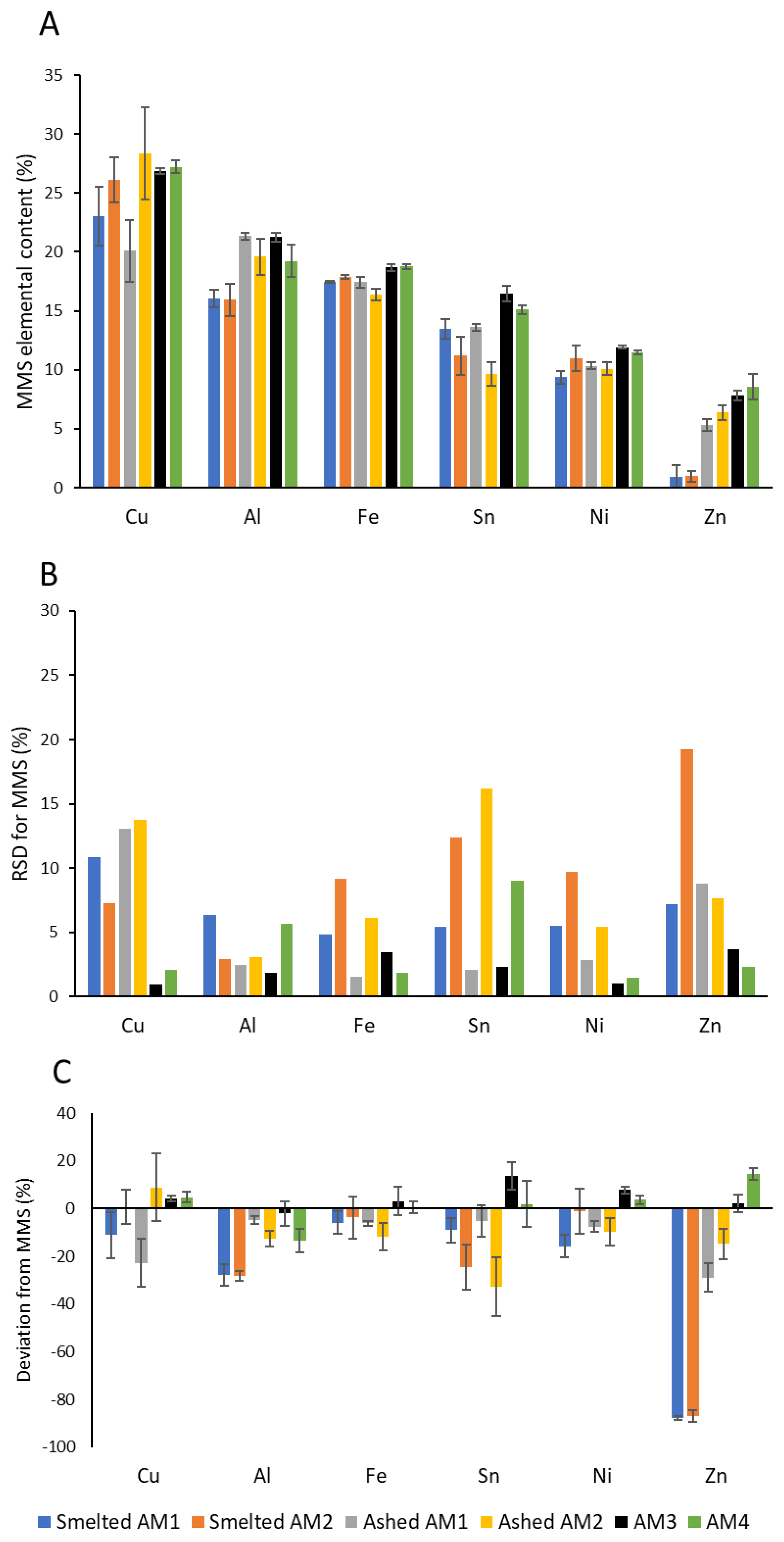
3.7. Use of Mixed-Metal Standards

Due to the high heterogeneity of PCBs, it is difficult to compare results from various publications and obtain reliable composition results for PCBs. Previous studies have used various types of PCBs, sample masses, and digestion processes as well as analytical instruments (Table 2). Currently, there is no standard protocol to reliably determine the elemental content of PCBs. A large hurdle is the lack of certified reference materials (RMs) [19,22]. RMs can be used to ensure the accuracy of results for method validation, determination of heterogeneity of sample material, and quality control [22].
The need for reliable RM has increasingly been recognised [19,20,53]. However, the production and use of RMs for PCBs are difficult due to the variability of the plastics, ceramics, and metals content in PCBs. A recent study has developed a standard waste PCB material to determine the accuracy of various analytical methods and to determine the optimal conditions for the characterisation of PCBs [19,22]. This was one of the first studies to use waste PCB material to create a RM. However, there is still a high degree of uncertainty for some of the metals of interest (14.08 + −5.67% mass of Cu). Bundesanstalt für Material-Forschung und-Prüfung (BAM), a material research institute in Germany, has previously offered a commercial RM, ERM-EZ505, manufactured with electronic scrap melted with pyrite, with low variability (<0.11% for Cu) [20]. However, this RM only contains Cu and Ni-base metals and still requires a large sample size of 5 g. This RM has since been replaced with BAM-M505a, which has a lower level of uncertainty (0.04% for copper) but still lacks the complexity of PCB samples arising from the composition of plastics, silicates, and ceramics, and it lacks other important metals such as zinc, aluminium, and iron [82].
To further evaluate the precision and accuracy of the analytical processes investigated in this study, a mixed-metal standard (MMS) was specially formulated and created. A mixture of known masses of analytical-grade pure metal powders was analysed using the same AMs as used for the PCB sample characterisation. The MMS samples used for analysis had a similar total mass as the analysed PCB samples (Table 5). As the mass of each element present in the MMS was known, it was possible to calculate the deviation from the actual MMS contents and thus determine the accuracy of the analytical methods.
The metal contents of the MMS as analysed using the various methods are shown in Figure 6. MMS samples pretreated with smelting demonstrated a large loss of zinc due to the high-temperature processing used. AM1 for smelted MMS showed a significant deviation (p < 0.05) from the expected MMS content for tin, zinc, nickel, and aluminium. AM2 for smelted MMS showed a significant deviation (p < 0.05) from the expected MMS content for tin, zinc, and aluminium. All samples for AM1 after smelting had more than a 5% deviation from the expected MMS content, which demonstrates the lack of accuracy for the method. AM2 for smelted MMS had a deviation above 5% from the expected MMS content for aluminium, tin, and zinc, demonstrating the lack of accuracy for these metals. All the metals analysed using AM1 and AM2 after smelting reported a loss of mass except for copper in AM2 after smelting. Based on these results, smelting can reduce the accuracy of analytical results for PCBs.
Ashed samples analysed by XRF and ICP-OES also demonstrated a large loss of mass for all metals except for copper with AM2 (Figure 6). AM1 after ashing showed a significant deviation (p < 0.05) from the expected MMS content for all metals except for tin and aluminium. AM2 after ashing showed a significant deviation (p < 0.05) from the expected MMS content for all metals except for nickel and copper. All metals analysed with AM1 and AM2 after ashing had more than a 5% deviation from the expected MMS content, except for aluminium in AM2. This indicates that ashing samples may reduce the accuracy of analytical results for PCBs. It remains unclear why there was such a large deviation from the expected metal contents. The temperature at which ashing occurred should not volatilise any metals, and the digestion method used should be sufficient to digest the metals. No residue was reported for any of these samples. One contributing factor could be the multiple steps involved for samples submitted for analysis using ICP-OES and XRF. Possibly, some of the material was lost during the extensive processing of the samples due to handling errors. Given the small sample masses (3.375 g) that were submitted for ashing, this error could result in a large loss of sample.
In contrast to samples that were pre-processed using ashing or smelting and analysed using AM1 and AM2, the AM3 showed a lower deviation from the expected MMS contents (Figure 6). For AM3, there was significant variation from the expected content (p < 0.05) for all metals except iron and zinc. However, the deviation from the expected MMS content was lower than detected for pre-processed samples, with tin and nickel having the highest deviations at 13.67% and 7.86%, respectively. The RSD for results from AM3 was also lower compared to AM1 and AM2 after ashing or smelting. However, the RSD from AM3 was still higher than what has been recorded in previous studies [82]. However, the deviation from the expected MMS content for copper was lower than reported for other previously tested analytical methods [19]. The reduced deviation from the actual content of the MMS for AM3 indicates that this method is more accurate compared to pre-treatment using ashing or smelting followed by ICP-OES or XRF.
AM4 also had a lower deviation from the MMS compared to AM1 and AM2 after ashing or smelting (Figure 6). There was a significant difference (p < 0.05) from the expected MMS content for all metals except tin and iron. However, all metals had a <5% deviation from the expected MMS content except for zinc and aluminium, which had deviations of 14.36% and −13.47%, respectively. Although the deviations from the expected MMS content were in the same range as reported previously [19], the deviations were still larger compared to that of BAM-M505a, which was certified using a range of analytical instruments from multiple laboratories. However, among the evaluated methods, AM4 had the lowest deviation from the expected MMS content, indicating that this AM had the highest degree of accuracy.
By using MMS samples for the same AMs as PCB samples, it was possible to compare the accuracy of the AMs. MMS samples pretreated using smelting and ashing showed a large deviation from the expected metal content. Samples without any pre-processing showed less deviation from the expected MMS content and hence a higher degree of accuracy. The MMS could be further customised to mimic PCB waste by adding plastics, glass, and ceramics to the material. Metals have been shown to be encapsulated and bound to plastics, glass, and ceramics, which can inhibit the solubilisation of these metals. The MMS used in this study did not have this limitation, and hence metals were directly exposed to leaching agents, reducing the complexity of the analytical process. Future work should investigate the possibility of including plastics, glass, and ceramics components in the RM. An alternative possibility could also be to include an internal standard within the waste PCB samples that could be tracked throughout the process to determine the accuracy of the AMs. Recent work has demonstrated the need for accurate and reliable RMs. This could facilitate the cross-study comparison of results and could potentially help to develop a standard protocol for the characterisation of PCBs. Despite the importance of using RM, only a few studies have used such material for PCB characterisation [19,20,22]. Further research is required to create accurate RMs that would be readily accessible.

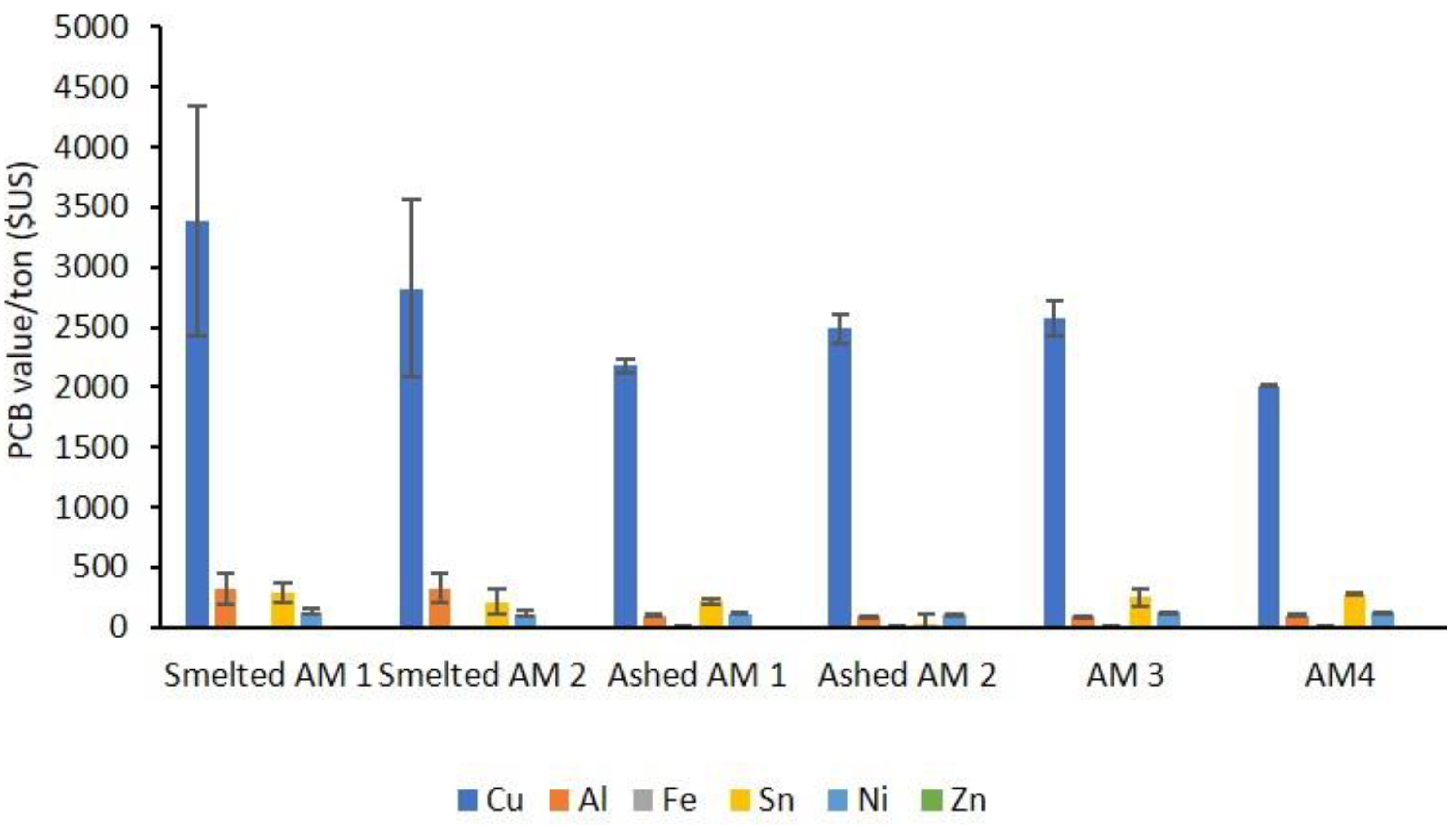
3.8. Variation in PCB Value Based on Analytical Methods

It is important to develop accurate and precise AMs for the quantification of metal content in PCBs to enable the determination of metal inputs and flows in PCB processing. At a research level, the initial quantification of metals in PCB samples is critical, as this is often used to determine the metal yield of various processes. If the initial content is overestimated, the process could be reporting an underestimated yield. If the content is underestimated, the reported yield might be overestimated.
When processing shredded PCBs with a ring mill followed by sieving, a range of particle sizes were recovered. The percent mass of the three size fractions of the PCBs were 67.19% <365 μm, 17.68% 365–500 μm, and 15.11% 500–750 μm. Figure 7 shows the total content of the selected metals in the PCBs considering the metal contents of the three-size fractions. The difference between the total elemental content based on the AM complicates the comparison of PCB compositions in the literature. It is therefore important to not only standardise an AM but also create a suitable RM to compare different analytical methods.
Knowing the precise metals composition of PCBs is crucial for calculating the value of the feedstock. PCBs can be classified as high grade, medium grade, or low grade based on the metal content [14]. The suppliers of waste PCBs are typically paid based on the metal value of the PCB waste. The variation in the metal content based on the AM can cause a large change in the total value of the PCBs (Figure 8). This variation in the value of the waste PCBs can be notable when considering the large processing capacity of some of the PCB processing facilities.

4. Conclusions

The accurate characterisation of waste PCB samples is of critical importance. The plastic, ceramic, and metal content of PCBs can notably vary in different particle sizes. Smaller particles sizes are more homogenous and hence typically result in lower RSDs when analysing metal content when compared to larger particle sizes. However, there is a limit on the size reduction achievable, and smaller particles have a larger plastic content, which can change the behaviour of the waste PCB samples.
Following particle screening, pre-treatment of the waste PCBs is an option. Smelting allowed for larger sample sizes, and analysis showed larger content for metals such as copper; however, the volatilisation of zinc at the smelting temperature and the formation of MBr species from BFR resulted in large RSDs, making the results less precise and more unreliable. Ashing provided an alternative that combusted the organic material present without causing the volatilisation of metal species. The precision for AM1 and AM2 after ashing was higher compared to smelting, and, as such, ashing can be a more-effective pre-treatment. The most precise analytical method examined in this study was AM4, which had the lowest RSD. This method can be further enhanced by increasing the sample mass and increasing the number of replicates.
The use of a MMS as a RM was investigated to compare the accuracy of the methods used. An accurate RM would allow for cross-study comparison and provide additional validation of AMs. Based on these results, AM4 had the highest degree of accuracy among the tested methods. Additional research is required to create a suitable RM that represents the complexity of waste PCB material.
This study highlighted the importance of understanding the composition of PCBs. The selection of an appropriate AM can allow for a comprehensive understanding of the feed material and its value and can enable the accurate tracking of metal species throughout the metal extraction process.

Supplementary Materials

The following are available online at https://www.mdpi.com/article/10.3390/met11121935/s1, Supplementary Figures S1–S3: Scanning electron microscopy (SEM) images showing specific locations of the resin blocks (A-C) and the resulting specific spectral peaks at the specific locations after EDS analysis used in determining elemental composition of PCB for the <365 μm fraction size.

Author Contributions

Conceptualisation, J.V.Y., K.Y.C., N.J.B. and A.H.K.; formal analysis, J.V.Y. and C.S.; funding acquisition, J.V.Y., K.Y.C., N.J.B., A.N.N., N.R.M. and A.H.K.; investigation, J.V.Y.; methodology, J.V.Y., K.Y.C., N.J.B., C.S. and A.H.K.; project administration, N.R.M. and A.H.K.; resources, A.H.K.; supervision, K.Y.C., N.J.B., A.N.N., N.R.M. and A.H.K.; visualisation, J.V.Y.; writing—original draft preparation, J.V.Y., C.S.; writing—review and editing, J.V.Y., K.Y.C., N.J.B., A.N.N., N.R.M. and A.H.K. All authors have read and agreed to the published version of the manuscript.

Funding

This research was funded by the New South Wales Government, through its Environmental Trust; by the State of Western Australia, through its New Industries Fund; and by CSIRO Land and Water. Jonovan Van Yken was funded by Murdoch University through the Research Training Scholarship and the CSIRO Research Office through a top-up scholarship.

Institutional Review Board Statement

Not applicable.

Informed Consent Statement

Not applicable.

Data Availability Statement

Not applicable.

Acknowledgments

The Department of Jobs, Tourism, Science, and Innovation does not endorse any information, product, process, or outcome arising from or in relation to the project. The authors thank Michael Somerville, Steve Peacock, Peter Austin, and Martijn Woltering for help in PCB and MMS characterization.

Conflicts of Interest

The authors declare no conflict of interest.

References

  1. Van Yken, J.; Boxall, N.J.; Cheng, K.Y.; Nikoloski, A.N.; Moheimani, N.R.; Kaksonen, A.H. E-waste recycling and resource recovery: A review on technologies, barriers and enablers with a focus on oceania. Metals 2021, 11, 1313. [Google Scholar] [CrossRef]
  2. Forti, V.; Balde, C.P.; Kuehr, R.; Bel, G. The Global E-Waste Monitor 2020: Quantities, Flows and the Circular Economy Potential; United Nations University/United Nations Institute for Training and Research: Bonn, Germany; International Telecommunication Union: Geneva, Switzerland; International Solid Waste Association: Rotterdam, The Netherlands, 2020; ISBN 9789280891140. [Google Scholar]
  3. Ilankoon, I.M.S.K.; Ghorbani, Y.; Chong, M.N.; Herath, G.; Moyo, T.; Petersen, J. E-waste in the international context—A review of trade flows, regulations, hazards, waste management strategies and technologies for value recovery. Waste Manag. 2018, 82, 258–275. [Google Scholar] [CrossRef]
  4. Kaya, M. Current WEEE Recycling Solutions; Elsevier: Amsterdam, The Netherlands, 2018; ISBN 9780081020579. [Google Scholar]
  5. Thakur, P.; Kumar, S. Metallurgical processes unveil the unexplored “sleeping mines” e-waste: A review. Environ. Sci. Pollut. Res. 2020, 27, 32359–32370. [Google Scholar] [CrossRef] [PubMed]
  6. Rautela, R.; Arya, S.; Vishwakarma, S.; Lee, J.; Kim, K.-H.; Kumar, S. E-waste Management and its Effects on the Environment and Human Health. Sci. Total Environ. 2021, 773, 145623. [Google Scholar] [CrossRef]
  7. Grant, K.; Goldizen, F.C.; Sly, P.D.; Brune, M.N.; Neira, M.; van den Berg, M.; Norman, R.E. Health consequences of exposure to e-waste: A systematic review. Lancet Glob. Health 2013, 1, e350–e361. [Google Scholar] [CrossRef] [Green Version]
  8. Deng, W.J.; Louie, P.K.K.; Liu, W.K.; Bi, X.H.; Fu, J.M.; Wong, M.H. Atmospheric levels and cytotoxicity of PAH’s and heavy metals in TSP and PM2.5 at an electronic waste recycling site in southeast China. Atmos. Environ. 2006, 40, 6945–6955. [Google Scholar] [CrossRef]
  9. Tue, N.M.; Takahashi, S.; Suzuki, G.; Isobe, T.; Viet, P.H.; Kobara, Y.; Seike, N.; Zhang, G.; Sudaryanto, A.; Tanabe, S. Contamination of indoor dust and air by polychlorinated biphenyls and brominated flame retardants and relevance of non-dietary exposure in Vietnamese informal e-waste recycling sites. Environ. Int. 2013, 51, 160–167. [Google Scholar] [CrossRef]
  10. Ha, N.N.; Agusa, T.; Ramu, K.; Tu, N.P.C.; Murata, S.; Bulbule, K.A.; Parthasaraty, P.; Takahashi, S.; Subramanian, A.; Tanabe, S. Contamination by trace elements at e-waste recycling sites in Bangalore, India. Chemosphere 2009, 76, 9–15. [Google Scholar] [CrossRef]
  11. Singh, M.; Thind, P.S.; John, S. Health risk assessment of the workers exposed to the heavy metals in e-waste recycling sites of Chandigarh and Ludhiana, Punjab, India. Chemosphere 2018, 203, 426–433. [Google Scholar] [CrossRef]
  12. Luo, C.; Liu, C.; Wang, Y.; Liu, X.; Li, F.; Zhang, G.; Li, X. Heavy metal contamination in soils and vegetables near an e-waste processing site, south China. J. Hazard. Mater. 2011, 186, 481–490. [Google Scholar] [CrossRef]
  13. Sum, E. The recovery of metals from electronic scrap. Rev. Extr. Metall. 1991, 43, 53–61. [Google Scholar] [CrossRef]
  14. Hagelüken, C. Recycling of electronic scrap at Umicore’s integrated metals smelter and refinery. Proc. Eur. Metall. Conf. EMC 2005, 1, 307–323. [Google Scholar]
  15. Kaya, M. Recovery of metals and nonmetals from electronic waste by physical and chemical recycling processes. Waste Manag. 2016, 57, 64–90. [Google Scholar] [CrossRef]
  16. Das, S.; Ting, Y.-P. Evaluation of Wet Digestion Methods for Quantification of Metal Content in Electronic. Resources 2017, 6, 64. [Google Scholar] [CrossRef] [Green Version]
  17. Korf, N.; Løvik, A.N.; Figi, R.; Schreiner, C.; Kuntz, C.; Martin, P.; Rösslein, M.; Wäger, P.; Susanne, V. Multi-element chemical analysis of printed circuit boards—Challenges and pitfalls. Waste Manag. 2019, 92, 124–136. [Google Scholar] [CrossRef] [PubMed]
  18. Tunali, M.; Tunali, M.M.; Yenigun, O. Characterization of different types of electronic waste: Heavy metal, precious metal and rare earth element content by comparing different digestıon methods. J. Mater. Cycles Waste Manag. 2021, 23, 149–157. [Google Scholar] [CrossRef]
  19. Andrade, D.F.; Machado, R.C.; Bacchi, M.A.; Pereira-Filho, E.R. Proposition of electronic waste as a reference material—Part 1: Sample preparation, characterization and chemometric evaluation. J. Anal. At. Spectrom. 2019, 34, 2394–2401. [Google Scholar] [CrossRef]
  20. Bookhagen, B.; Obermaier, W.; Opper, C.; Koeberl, C.; Hofmann, T.; Prohaska, T.; Irrgeher, J. Analytical Methods Development of a versatile analytical protocol for the comprehensive determination of the elemental composition of smartphone compartments on the example of printed circuit boards. Anal. Methods 2018, 10, 3864–3871. [Google Scholar] [CrossRef]
  21. Mičková, V.; Ružičková, S.; Remeteiová, D.; Laubertová, M.; Dorková, M. Sampling and digestion of waste mobile phones printed circuit boards for Cu, Pb, Ni, and Zn determination. Chem. Pap. 2018, 72, 1231–1238. [Google Scholar] [CrossRef]
  22. Andrade, D.F.; Machado, R.C.; Pereira-Filho, E.R. Proposition of electronic waste as a reference material—Part 2: Homogeneity, stability, characterization, and uncertainties. J. Anal. At. Spectrom. 2019, 34, 2402–2410. [Google Scholar] [CrossRef]
  23. Huang, J.; Chen, M.; Chen, H.; Chen, S.; Sun, Q. Leaching behavior of copper from waste printed circuit boards with Brønsted acidic ionic liquid. Waste Manag. 2014, 34, 483–488. [Google Scholar] [CrossRef]
  24. Arshadi, M.; Mousavi, S.M. Multi-objective optimization of heavy metals bioleaching from discarded mobile phone PCBs: Simultaneous Cu and Ni recovery using Acidithiobacillus ferrooxidans. Sep. Purif. Technol. 2015, 147, 210–219. [Google Scholar] [CrossRef]
  25. Bai, J.; Gu, W.; Dai, J.; Zhang, C.; Yuan, W.; Deng, M.; Luo, X.; Wang, J. The Catalytic Role of Nitrogen-Doped Carbon Nanotubes in Bioleaching Copper from Waste Printed Circuit Boards. Pol. J. Environ. Stud. 2016, 25, 951–957. [Google Scholar] [CrossRef]
  26. Bas, A.D.; Deveci, H.; Yazici, E.Y. Bioleaching of copper from low grade scrap TV circuit boards using mesophilic bacteria. Hydrometallurgy 2013, 138, 65–70. [Google Scholar] [CrossRef]
  27. Bryan, C.G.; Watkin, E.L.; McCredden, T.J.; Wong, Z.R.; Harrison, S.T.L.; Kaksonen, A.H. The use of pyrite as a source of lixiviant in the bioleaching of electronic waste. Hydrometallurgy 2015, 152, 33–43. [Google Scholar] [CrossRef]
  28. Chen, S.; Yang, Y.; Liu, C.; Dong, F.; Liu, B. Column bioleaching copper and its kinetics of waste printed circuit boards ( WPCBs ) by Acidithiobacillus ferrooxidans. Chemosphere 2015, 141, 162–168. [Google Scholar] [CrossRef]
  29. Gu, W.; Bai, J.; Dong, B.; Zhuang, X.; Zhao, J. Catalytic effect of graphene in bioleaching copper from waste printed circuitboards by Acidithiobacillus ferrooxidans. Hydrometallurgy 2017, 171, 172–178. [Google Scholar] [CrossRef]
  30. Gu, W.; Bai, J.; Dong, B.; Zhuang, X.; Zhao, J.; Zhang, C.; Wang, J.; Shih, K. Enhanced bioleaching efficiency of copper from waste printed circuit board driven by nitrogen-doped carbon nanotubes modified electrode. Chem. Eng. J. 2017, 324, 122–129. [Google Scholar] [CrossRef]
  31. Guezennec, A.G.; Bru, K.; Jacob, J.; D’Hugues, P. Co-processing of sulfidic mining wastes and metal-rich post-consumer wastes by biohydrometallurgy. Miner. Eng. 2015, 75, 45–53. [Google Scholar] [CrossRef] [Green Version]
  32. Ilyas, S.; Anwar, M.A.; Niazi, S.B.; Afzal Ghauri, M. Bioleaching of metals from electronic scrap by moderately thermophilic acidophilic bacteria. Hydrometallurgy 2007, 88, 180–188. [Google Scholar] [CrossRef]
  33. Ilyas, S.; Ruan, C.; Bhatti, H.N.; Ghauri, M.A.; Anwar, M.A. Column bioleaching of metals from electronic scrap. Hydrometallurgy 2010, 101, 135–140. [Google Scholar] [CrossRef]
  34. Ilyas, S.; Lee, J.C.; Chi, R.A. Bioleaching of metals from electronic scrap and its potential for commercial exploitation. Hydrometallurgy 2013, 131–132, 138–143. [Google Scholar] [CrossRef]
  35. Ilyas, S.; Lee, J.C. Bioleaching of metals from electronic scrap in a stirred tank reactor. Hydrometallurgy 2014, 149, 50–62. [Google Scholar] [CrossRef]
  36. Liang, G.; Mo, Y.; Zhou, Q. Novel strategies of bioleaching metals from printed circuit boards (PCBs) in mixed cultivation of two acidophiles. Enzym. Microb. Technol. 2010, 47, 322–326. [Google Scholar] [CrossRef]
  37. Liang, G.; Tang, J.; Liu, W.; Zhou, Q. Optimizing mixed culture of two acidophiles to improve copper recovery from printed circuit boards (PCBs). J. Hazard. Mater. 2013, 250–251, 238–245. [Google Scholar] [CrossRef]
  38. Mäkinen, J.; Bachér, J.; Kaartinen, T.; Wahlström, M.; Salminen, J. The effect of flotation and parameters for bioleaching of printed circuit boards. Miner. Eng. 2015, 75, 26–31. [Google Scholar] [CrossRef]
  39. Priya, A.; Hait, S. Extraction of metals from high grade waste printed circuit board by conventional and hybrid bioleaching using Acidithiobacillus ferrooxidans. Hydrometallurgy 2018, 177, 132–139. [Google Scholar] [CrossRef]
  40. Rodrigues, M.L.M.; Leão, V.A.; Gomes, O.; Lambert, F.; Bastin, D.; Gaydardzhiev, S. Copper extraction from coarsely ground printed circuit boards using moderate thermophilic bacteria in a rotating-drum reactor. Waste Manag. 2015, 41, 148–158. [Google Scholar] [CrossRef]
  41. Brandl, H.; Bosshard, R.; Wegmann, M. Computer-munching microbes: Metal leaching from electronic scrap by bacteria and fungi. Process Metall. 1999, 9, 569–576. [Google Scholar] [CrossRef]
  42. Xiang, Y.; Wu, P.; Zhu, N.; Zhang, T.; Liu, W.; Wu, J.; Li, P. Bioleaching of copper from waste printed circuit boards by bacterial consortium enriched from acid mine drainage. J. Hazard. Mater. 2010, 184, 812–818. [Google Scholar] [CrossRef]
  43. Shah, M.B.; Tipre, D.R.; Purohit, M.S.; Dave, S.R. Development of two-step process for enhanced biorecovery of Cu-Zn-Ni from computer printed circuit boards. J. Biosci. Bioeng. 2015, 120, 167–173. [Google Scholar] [CrossRef]
  44. Silva, R.A.; Park, J.; Lee, E.; Park, J.; Choi, S.Q.; Kim, H. Influence of bacterial adhesion on copper extraction from printed circuit boards. Sep. Purif. Technol. 2015, 143, 169–176. [Google Scholar] [CrossRef]
  45. Yang, T.; Xu, Z.; Wen, J.; Yang, L. Factors influencing bioleaching copper from waste printed circuit boards by Acidithiobacillus ferrooxidans. Hydrometallurgy 2009, 97, 29–32. [Google Scholar] [CrossRef]
  46. Wang, J.; Bai, J.; Xu, J.; Liang, B. Bioleaching of metals from printed wire boards by Acidithiobacillus ferrooxidans and Acidithiobacillus thiooxidans and their mixture. J. Hazard. Mater. 2009, 172, 1100–1105. [Google Scholar] [CrossRef]
  47. Wang, S.; Zheng, Y.; Yan, W.; Chen, L.; Dummi Mahadevan, G.; Zhao, F. Enhanced bioleaching efficiency of metals from E-wastes driven by biochar. J. Hazard. Mater. 2016, 320, 393–400. [Google Scholar] [CrossRef]
  48. Yang, Y.; Chen, S.; Li, S.; Chen, M.; Chen, H.; Liu, B. Bioleaching waste printed circuit boards by Acidithiobacillus ferrooxidans and its kinetics aspect. J. Biotechnol. 2014, 173, 24–30. [Google Scholar] [CrossRef]
  49. Minkkinen, P. Practical applications of sampling theory. Chemom. Intell. Lab. Syst. 2004, 74, 85–94. [Google Scholar] [CrossRef]
  50. Touze, S.; Guignot, S.; Hubau, A.; Devau, N.; Chapron, S. Sampling waste printed circuit boards: Achieving the right combination between particle size and sample mass to measure metal content. Waste Manag. 2020, 118, 380–390. [Google Scholar] [CrossRef]
  51. Havlik, T.; Orac, D.; Petranikova, M.; Miskufova, A.; Kukurugya, F.; Takacova, Z. Leaching of copper and tin from used printed circuit boards after thermal treatment. J. Hazard. Mater. 2010, 183, 866–873. [Google Scholar] [CrossRef]
  52. Gy, P. Sampling of Particulate Materials Theory and Practice; Elsevier: Amsterdam, The Netherlands, 2012; ISBN 044460135X. [Google Scholar]
  53. Touzé, S.; Chapron, S.; Hubau, A.; Guignot, S. Characterization of printed circuit boards waste -influence of sample mass and particle size—Example of zinc and nickel content. In Proceedings of the WasteEng Conference, Virtual Mode, Gueph, ON, Canada, 31 May–4 June 2021. [Google Scholar]
  54. Ghodrat, M.; Rhamdhani, M.A.; Khaliq, A.; Brooks, G.; Samali, B. Thermodynamic analysis of metals recycling out of waste printed circuit board through secondary copper smelting. J. Mater. Cycles Waste Manag. 2018, 20, 386–401. [Google Scholar] [CrossRef]
  55. Anindya, A.; Swinbourne, D.; Reuter, M.; Matusewicz, R. Tin distribution during smelting of WEEE with copper scrap. Proc. Eur. Metall. Conf. EMC 2009, 2, 555–568. [Google Scholar]
  56. Somerville, M.A.; Kolton, P. High Temperature Characterisation and Techno-Economics of E-Waste Processing. In REWAS 2016; Springer: Singapore, 2016; pp. 297–302. [Google Scholar]
  57. Sornlar, W.; Choeycharoen, P.; Wannagon, A. Characterization of alumina crucible made from aluminum industrial waste. J. Aust. Ceram. Soc. 2020, 56, 771–779. [Google Scholar] [CrossRef]
  58. RADAK Crucible Selection Guide. Available online: https://luxel.com/wp-content/uploads/2017/08/Crucible-Selection-Guide-Rev.08-2017.pdf (accessed on 11 July 2021).
  59. Barontini, F.; Cozzani, V.; Marsanich, K.; Raffa, V.; Petarca, L. An experimental investigation of tetrabromobisphenol A decomposition pathways. J. Anal. Appl. Pyrolysis 2004, 72, 41–53. [Google Scholar] [CrossRef]
  60. Hennebert, P.; Filella, M. WEEE plastic sorting for bromine essential to enforce EU regulation. Waste Manag. 2018, 71, 390–399. [Google Scholar] [CrossRef] [PubMed]
  61. Oleszek, S.; Grabda, M.; Shibata, E.; Nakamura, T. Distribution of copper, silver and gold during thermal treatment with brominated flame retardants. Waste Manag. 2013, 33, 1835–1842. [Google Scholar] [CrossRef]
  62. Barontini, F.; Cozzani, V. Formation of hydrogen bromide and organobrominated compounds in the thermal degradation of electronic boards. J. Anal. Appl. Pyrolysis 2006, 77, 41–55. [Google Scholar] [CrossRef]
  63. Marsanich, K.; Zanelli, S.; Barontini, F.; Cozzani, V. Evaporation and thermal degradation of tetrabromobisphenol A above the melting point. Thermochim. Acta 2004, 421, 95–103. [Google Scholar] [CrossRef]
  64. Kailasa, S.K.; Chemistry, A. Inorganic Contaminants: Sample Preparation Approaches; Elsevier: Amsterdam, The Netherlands, 2012; Volume 3, ISBN 9780123813732. [Google Scholar]
  65. Birloaga, I.; Michelis, I.D.; Ferella, F.; Buzatu, M.; Vegliò, F. Study on the influence of various factors in the hydrometallurgical processing of waste printed circuit boards for copper and gold recovery. Waste Manag. 2013, 33, 935–941. [Google Scholar] [CrossRef]
  66. Das, P.; Gabriel, J.-C.P.; Tay, C.Y.; Lee, J.-M. Value-added products from thermochemical treatments of contaminated e-waste plastics. Chemosphere 2021, 269, 129409. [Google Scholar] [CrossRef] [PubMed]
  67. Rutkowski, J.V.; Levin, B.C. Acrylonitrile–butadiene–styrene copolymers (ABS): Pyrolysis and combustion products and their toxicity—A review of the literature. Fire Mater. 1986, 10, 93–105. [Google Scholar] [CrossRef] [Green Version]
  68. Periodic Table Elemental Stability. Available online: https://www.inorganicventures.com/periodic-table (accessed on 25 May 2021).
  69. Hoenig, M. Sample dissolution for elemental analysis|Dry ashing. In Encyclopedia of Analytical Science, 2nd ed.; Worsfold, P., Townshend, A., Poole, C., Eds.; Elsevier: Oxford, UK, 2005; pp. 131–136. ISBN 978-0-12-369397-6. [Google Scholar]
  70. Hirokawa, Y.; Shibata, Y.; Konya, T. X-ray fluorescence analysis of Co, Ni, Pd, Ag, and Au in the scrapped printed-circuit-board. X-ray Spectrom. 2013, 43, 134–140. [Google Scholar] [CrossRef]
  71. Detection Limit Guidance Inductively Coupled Plasma Spectroscopy. Available online: http://www.nanoscience.co.jp/surface_analysis/pdf/icp-oes-ms-detection-limit-guidance-BR023.pdf (accessed on 11 July 2021).
  72. Chemical Resistance Chart. Available online: https://www.plasticsintl.com/chemical-resistance-chart (accessed on 16 July 2021).
  73. Kumar, M.; Lee, J.C.; Kim, M.S.; Jeong, J.; Yoo, K. Leaching of metals from waste printed circuit boards (WPCBs) using sulfuric and nitric acids. Environ. Eng. Manag. J. 2014, 13, 2601–2607. [Google Scholar] [CrossRef]
  74. Jha, M.K.; Lee, J.C.; Kumari, A.; Choubey, P.K.; Kumar, V.; Jeong, J. Pressure leaching of metals from waste printed circuit boards using sulfuric acid. Jom 2011, 63, 29–32. [Google Scholar] [CrossRef]
  75. Urben, P. Bretherick’s Handbook of Reactive Chemical Hazards; Elsevier: Amsterdam, The Netherlands, 2017; ISBN 0081010591. [Google Scholar]
  76. Jones, C.W. Applications of Hydrogen Peroxide and Derivatives; Royal Society of Chemistry: London, UK, 1999; Volume 2, ISBN 0854045368. [Google Scholar]
  77. Karaffa, L.S. The Merck Index: An Encyclopedia of Chemicals, Drugs, and Biologicals; RSC Publishing: London, UK, 2013; ISBN 1849736707. [Google Scholar]
  78. Zhu, X.; Cui, T.; Li, B.; Nie, C.; Zhang, H.; Lyu, X. Metal recovery from waste printed circuit boards by flotation technology with non-ionic renewable collector. J. Clean Prod. 2020, 255, 120289. [Google Scholar] [CrossRef]
  79. Helmenstine, A.A. Piranha Solution Preparation, Use, and Safety. Available online: https://sciencenotes.org/piranha-solution-preparation-use-and-safety/ (accessed on 26 May 2021).
  80. Mankhand, T.R.; Singh, K.K.; Gupta, S.K.; Das, S. Pyrolysis of Printed Circuit Boards. Int. J. Met. Eng. 2012, 1, 102–107. [Google Scholar] [CrossRef]
  81. Lin, K.; Chiang, H. Liquid oil and residual characteristics of printed circuit board recycle by pyrolysis. J. Hazard. Mater. 2014, 271, 258–265. [Google Scholar] [CrossRef]
  82. Certified Reference Material BAM-M505a. Available online: https://rrr.bam.de/RRR/Content/EN/Downloads/RM-Certificates/RM-cert-special-materials/bam_m505a_repe.pdf?__blob=publicationFile (accessed on 27 July 2021).
  83. Copper Commodity Price. Available online: https://markets.businessinsider.com/commodities/copper-price (accessed on 27 July 2021).
  84. Aluminium Commodity Price. Available online: https://markets.businessinsider.com/commodities/aluminum-price (accessed on 27 July 2021).
  85. Iron Commodity Price. Available online: https://markets.businessinsider.com/commodities/iron-ore-price (accessed on 27 July 2021).
  86. Tin Commodity Price. Available online: https://markets.businessinsider.com/commodities/tin-price (accessed on 27 July 2021).
  87. Nickel Commodity Price. Available online: https://markets.businessinsider.com/commodities/nickel-price (accessed on 27 July 2021).
  88. Zinc Commodity Price. Available online: https://markets.businessinsider.com/commodities/zinc-price (accessed on 27 July 2021).
Figure 1. Flowsheet for sample processing and analytical methods examined.
Metals 11 01935 g001
Figure 2. The content of (A) Cu, (B) Al, (C) Fe, (D) Sn, (E) Ni, and (F) Zn in the three PCB size fractions as determined by various analytical methods. Error bars show standard deviations between three replicate samples.
Metals 11 01935 g002
Figure 3. The RSD of PCB metal contents as determined by (A) ashing and AM1, (B) ashing and AM2, (C) smelting and AM1, (D) smelting and AM2, (E) AM3, and (F) AM4 for each particle size fraction. Error bars show standard deviations between three replicate samples.
Metals 11 01935 g003
Figure 4. Organic content of PCB samples as calculated based on loss on ignition (LOI) during smelting and ashing pre-treatments. Error bars show standard deviations between three replicate samples.
Metals 11 01935 g004
Figure 5. Scanning electron microscopy (SEM) images showing specific locations of the resin block (AC) used for determining elemental composition of PCBs for <365 μm fraction size with energy-dispersive X-ray spectroscopy (EDS) analysis as shown in Table 4. Details on the specific spectral peaks at these locations can be found in Supplementary Figures S1–S3.
Metals 11 01935 g005
Figure 6. The elemental content (A) and the relative standard deviation (RSD) (B) of the mixed-metal standard (MMS) and the deviation of detected results from the expected content (C). Error bars show the standard deviation of triplicate samples.
Metals 11 01935 g006
Figure 7. The total content of selected metals in the PCBs considering the metal contents of the three size fractions.
Metals 11 01935 g007
Figure 8. The different values of PCBs based on the AM used. PCB value was calculated based on the current market price for Cu [83], Al [84], Fe [85], Sn [86], Ni [87], and Zn [88] and the metal content of these elements in the PCB samples.
Metals 11 01935 g008
Table 1. Range of metal composition of PCBs in the literature (adapted from [1,2,4,15]).
ElementComposition (%)ElementComposition (ppm)
Cu6–40Au 250–2050
Fe1.2–8Ag 110–4500
Al0.3–7.2Pd 50–4000
Sn1–6.3Pt 5–30
Pb1–4.2Co 1–4000
Ni0.0024–5.4--
Zn0.04–2.2--
Sb0.1–0.4--
Table 2. Various analytical methods employed in the literature for e-waste characterisation and the corresponding elemental content of the e-waste.
Type of PCB SampleAnalytical Method Elemental Content (%)
Particle Size
(μm Unless Otherwise
Specified)
Sample Size (g)Digestion MethodAnalysis InstrumentCu Al Ni Zn Sn Fe Reference
ES 1 −14/+20 mesh1AR 2 AAS 319.11.380.040.81-0.002[23]
ES −14/+20 mesh1HNO3 AAS28.7-0.430.46-0.002[23]
MP 4 PCB 37–150 1AR ICP-OES 56.653.130.380.36-1.46[24]
MP PCB 1000–4000-AR ICP-OES 20.3–33.9 -4.8–0.913.2–1.46.2–3.2-[25]
TV PCB250-Wet chemical analysis -11.20.30.020.15-0.004[26]
PCB2000-Dry ashing + AR-3.38-0.412.191.2616.1[27]
ES4000–10000-AR -24.82.5---0.18[28]
ES<10001AR -20.3 4.83.26.2-[29]
ES <1000-AR ICP-OES20.3 4.3 4.3 [30]
ES <7503ARAAS21.5 -0.241.43.42.4[31]
ES 50–1501ARAAS8.50.712.08.00.000688.3[32]
ES 100–1201ARAAS8.90.752.08.20.000658[33]
ES 80-AR -90.752.18.4-8[34]
ES 105-AR ICP-MS 613.052.2852.0752.035-1.83[35]
ES 100–200-ARAAS12.61.42.45.6-1.2[36]
ES 100–200---12.61.42.45.6-1.2[37]
MP PCB 250--ICP-MS
ICP-OES
3.27 2.21.9--1.4[38]
PCB 75–1000-MW digestICP-MS20.9-0.0141.59--[39]
PCB147–2081AR ICP-MS28.0 0.070.41-0.51[40]
PCB dust 500-HNO3 ICP-OES ICP-MS8 237152623-[41]
ES 40 mesh 1HNO3, HCl, HF and H2O2ICP-OES23.1 2.60.1921.71.80.81[42]
ES -1AR
H2SO4
AAS304.5.384.59-6.01[43]
ES 500–1000---40.2---4.50.44[44]
ES 100–2002AR AAS12.61.42.45.6-1.2[36]
ES 500---25.1-0.0020.04-0.66[45]
PCB 350--ICP-OES9.0-0.010.21--[46]
PCB 3000--ICP-OES2.94-0.010.19--[46]
ES 80 mesh 0.1HNO3, HCl, HF and H2O2ICP-OES11.62.01----[47]
ES 20–40 mesh0.5 AR ICP-OES25.56.3.536.183.313.17[48]
1 ES: electronic scrap, 2 AR: aqua regia, 3 AAS: atomic absorption spectrometry, 4 MP: mobile phone, 5 ICP-OES: inductively coupled plasma optical emission spectroscopy, 6 ICP-MS: inductively coupled plasma mass spectrometry.
Table 3. Experimental conditions for the methods used for PCB characterisation.
Initial Sample Mass (g)Pre-Processing Analytical ProcessSample Mass for Digestion (g) Acid
Digestion
Temperature of Acid Digestion (°C)Pressure of Acid Digestion (bar) Fusion Digestion Analytical Instrument
2.5–3Ashing 1 10.2–0.3HNO31001YesXRF
2.5–3Ashing2 20.1Aqua regia, HF2001YesICP-OES
50 Smelting10.2–0.3HNO31001YesXRF
50Smelting20.1Aqua regia, HF2001YesICP-OES
1None3 30.1Aqua regia, H2SO4, H2O21001YesICP-OES
0.2None 4 40.2Aqua regia, HF, microwave digestion18030No ICP-OES
1 X-ray fluorescence of ashed/smelted samples, 2 ICP-OES analysis of ashed/smelted samples, 3 acid digestion and direct fusion digestion followed by ICP-OES, 4 microwave-assisted acid digestion followed by ICP-OES.
Table 4. The content of the most-dominant elements in PCB samples by weight at specific locations of the scanning electron microscopy (SEM) images as determined by energy-dispersive X-ray spectroscopy (EDS).
SEM ImageSEM-EDS PointElement Content by Weight (%)
COAlSiCaFeCuSn BaBr
A12.50.10002.195.3000
21.1000002.294.800
34.943.837.18.30.40.51.303.50
411.139.67.723.816.20.30.7000
B11.1000001.9394.600
21.043.3409.300.431.403.90
32.50.1000.40.2395.1000
C14520.88.300000025.7
22.70000097.3000
37.239.98.524.417.101.5000
Table 5. The expected average content of MMS based on the mass of sample analysed and the detected content based on various analytical methods.
ParameterAnalytical MethodAverage Elemental Content (%)
CuAl FeSnNiZn
Expected content from MMSSmelting AM125.92122.23318.52714.80911.1117.407
Smelting AM225.92122.23318.52714.80911.1117.407
Ashing AM125.99622.40418.56314.40411.1567.477
Ashing AM225.99622.40418.56314.40411.1567.477
AM325.470 21.940 18.116 14.506 11.338 7.541
AM425.95322.22818.49414.82411.0327.470
Detected content for MMSSmelting AM123.05216.03017.45213.4679.3640.915
Smelting AM226.12415.94017.85411.19610.9880.963
Ashing AM120.10521.34117.43413.60210.3205.321
Ashing AM228.34419.58616.3849.66410.0776.371
AM326.85621.28118.66416.46511.9257.802
AM427.22019.23318.75015.10011.4338.543
Deviation from MMSSmelting AM1−11.071−27.897−5.804−9.061−15.722−87.645
Smelting AM20.759−28.312−3.646−24.402−1.114−87.004
Ashing AM1−22.647−4.759−6.087−5.273−7.499−28.855
Ashing AM28.936−12.548−11.709−32.545−9.627−14.813
AM34.175−1.9733.20013.6767.8632.209
AM44.882−13.4740.4031.9083.65014.363
Publisher’s Note: MDPI stays neutral with regard to jurisdictional claims in published maps and institutional affiliations.

