Characterization of Magnetoelectropolished Stainless Steel Surfaces’ Texture by Using the Angle-Resolved Scattering and Image Processing Analysis Methods


Abstract
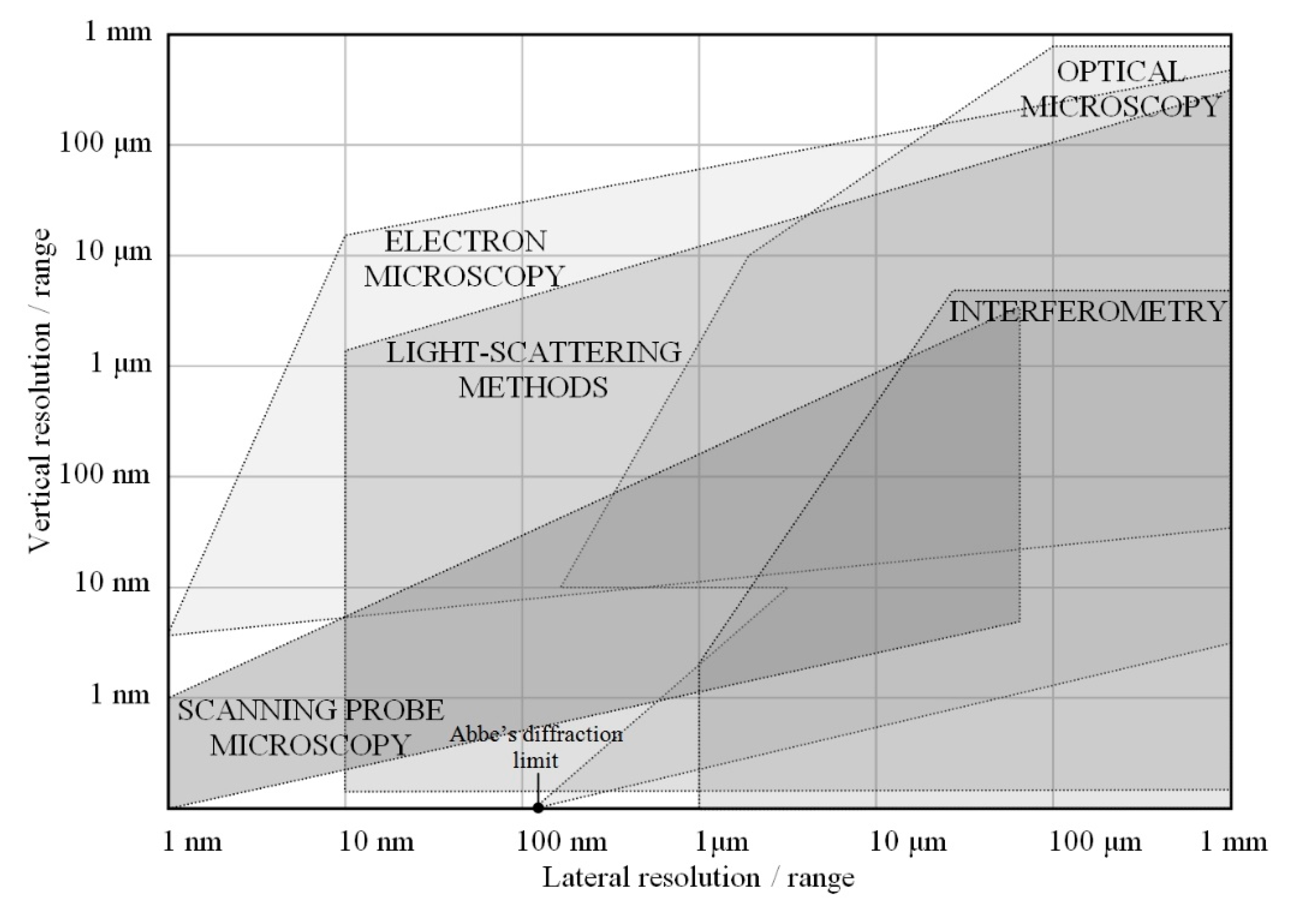
:1. Introduction
- relatively low heights of irregularities from approx. 0.2 to 200–300 nm (optical and opto-electronical elements, silicon wafers, tooth implants and artificial hip joint prosthesis stem balls),
- high heights of irregularities from approx. 500 to 1500–2000 nm (precisely machined machine parts, automotive components, medical devices elements and parts of aeronautical engines).
2. Methodology of Experimental Studies
2.1. Characteristics of the Samples
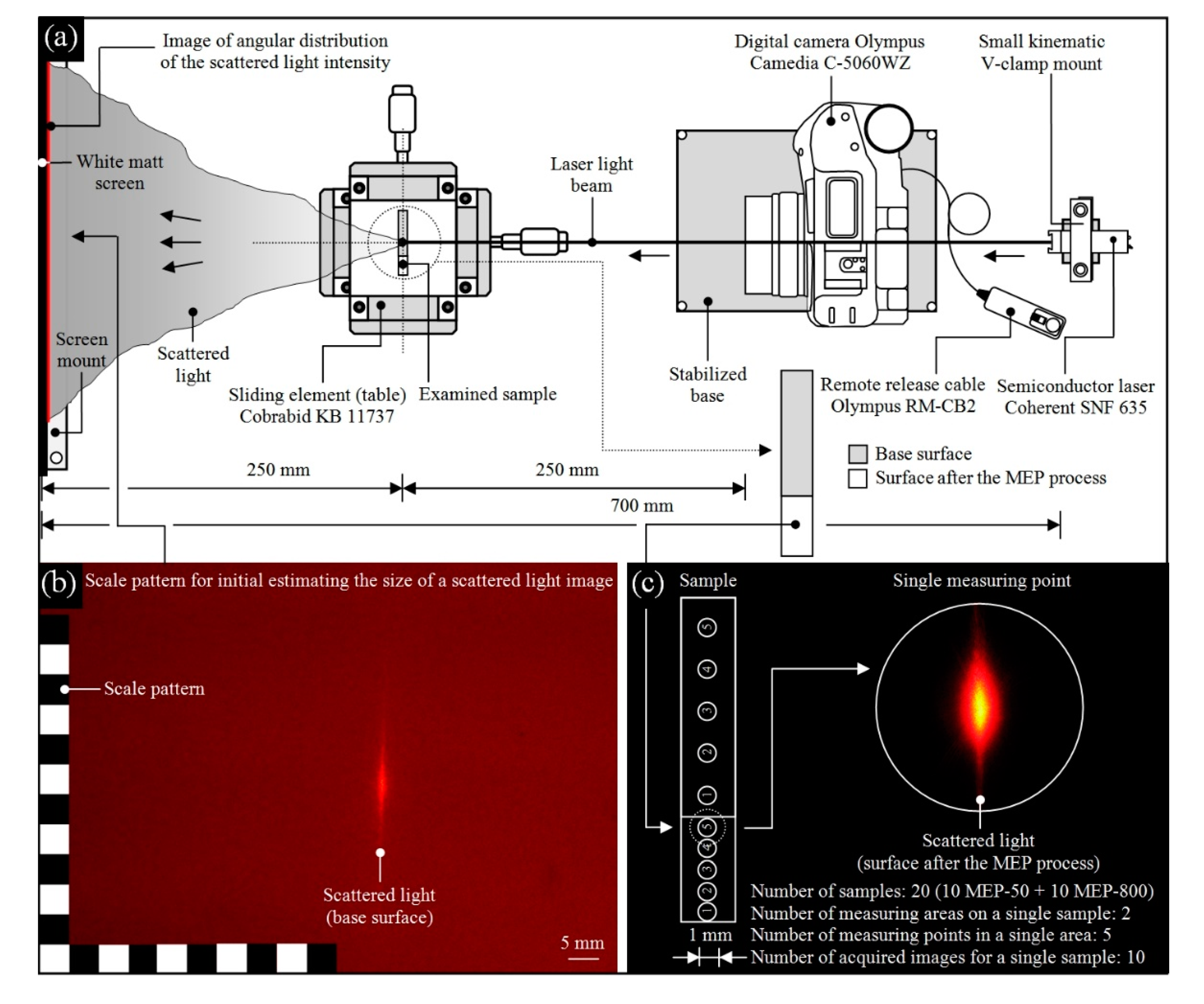
2.2. Acquisition of Digital Images of the Angular Distribution of Scattered Light Intensity
2.3. Characteristics of Image Processing and Analysis Process
3. Results and Discussion
4. Conclusions
- The AISI 316L stainless austenitic steel samples divided into two groups (each 10 samples) were electrochemically polished in a magnetic field: MEP-800 (magnetic field: 66 mT, current density: 800 A/dm2) and MEP-50 (magnetic field: 66 mT, current density: 500 A/dm2) (Section 2.1). The samples after the process were characterized by relatively smooth surface with small heights of the surface irregularities. The average value of Ra roughness (profile) parameter measured by optical profilometer Talysurf CLI 2000 with laser triangulation sensor LK-031 for all magnetoelectropolished surfaces was 0.823 μm.
- The obtained surface features were assessed by using one of the non-contact light-scattering methods for confirmation of correctness of carrying out the process. In this case, the angle-resolved scattering-based experimental setup was used. The surface of each sample was illuminated using a laser beam (wavelength λ = 635 nm, angle of incidence 50°) and its angular distribution in the observation plane was acquired as a digital image (Section 2.2). After pre-processing (ImageJ 1.57) images, we carried out parametric analysis (Image Pro®-Plus 5.1), which included the calculation of two key geo- and photometric parameters (Section 2.3).
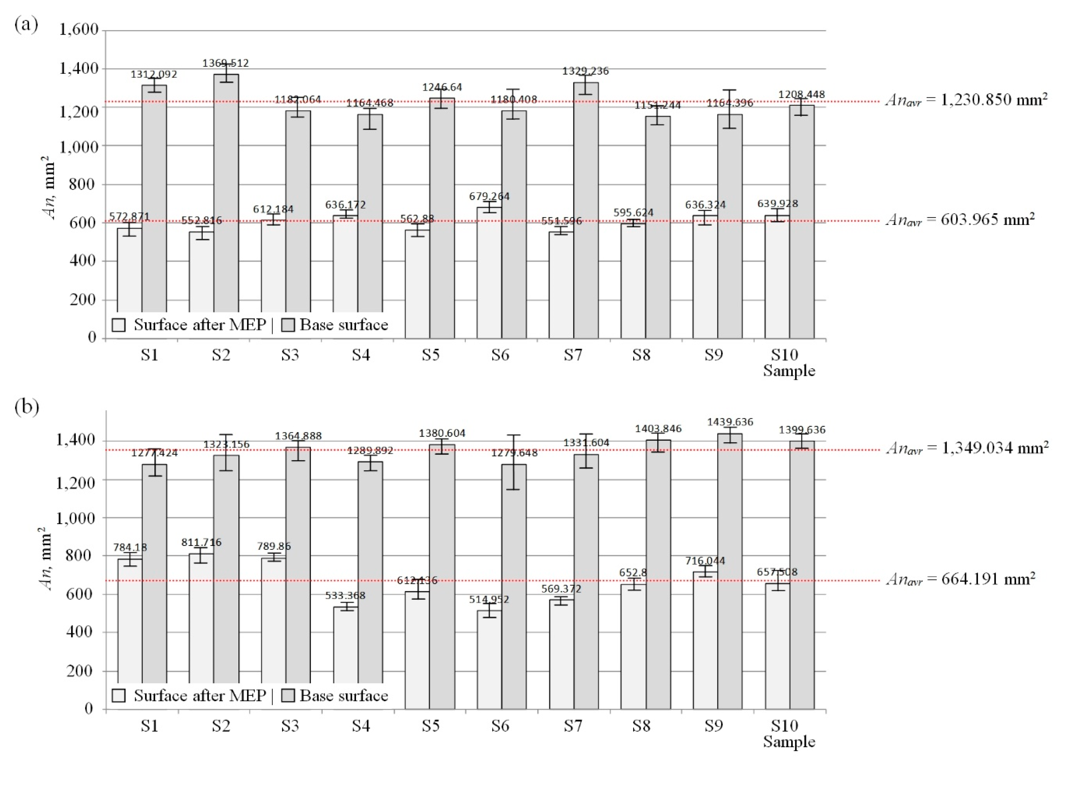
- The obtained values of area (of the bright regions of scattered light image) (Figure 5) and integrated optical density (of the bright regions of scattered light image) (Figure 6) were similar for the magnetoelectropolished surfaces of both types of samples. Additionally, we found that the above values (in each case) were approx. 50% lower (AnMEP—49% (MEP-800) and over 49% (MEP-50); IΣMEP—51% (MEP-800) and 54% (MEP-50), respectively) than those obtained for the base surface. This indicates a much smaller share of light scattering component at the gain of the specular reflection component. This is a very advantageous surface feature after the magnetoelectropolished process, especially useful in a wide range of industrial applications, in areas such as precision mechanical, chemical and biomedical engineering as well as opto- and microelectronics.
- Compared to electropolishing, the magnetoelectropolishing process is characterized by over 32% more effectiveness (Figure 7) at 27% lower surface roughness (Ra). The results obtained for this type of surface (in the context of their reflection properties and surface texture properties) are very promising, which encourages further work to improve this electrochemical polishing process and study its effects.
Author Contributions
Funding
Conflicts of Interest
Nomenclature
| AC | Alternating current |
| AFM | Atomic force microscopy |
| ARS | Angle-resolved scattering |
| BRDF | Bidirectional reflectance distribution function |
| BSDF | Bidirectional scatter distribution function |
| CCD | Charge-coupled device |
| CLSM | Confocal laser scanning microscopy |
| CMP | Conventional machine polishing |
| DC | Direct current |
| EP | Electropolishing |
| FVM | Focus variation microscopy |
| MEP | Magnetoelectropolishing |
| MFM | Mirror facet model |
| PSI | Phase shifting interferometry |
| SIM | Surface imperfections |
| SEM | Scanning electron microscopy |
| T-S | Torrence–Sparrow theory |
| A | Illuminated surface area |
| An | Area (of the bright regions of an image of scattered light) |
| dΦe | Radiant flux/power scattered within the solid angle |
| dΩ | Solid angle |
| An | Area (of the bright regions of an image of scattered light) |
| fx | Spatial frequency (x-axis) of the surface roughness |
| fy | Spatial frequency (y-axis) of the surface roughness |
| I(i, j) | Grey scale intensity |
| IΣ | Integrated optical density (of the bright regions of an image of scattered light) |
| i | Row number |
| j | Column number |
| Le | Scatter surface radiance |
| Q | Non-dimensional factor depending on the azimuthal scattering angle ϕ |
| Ra | Roughness average |
| S(fx, fy) | Two-dimensional surface power spectral density function |
| θi | Angle of incidence |
| θd | Scattering angle |
| λ | Wavelength of light |
| Φei | Radiant flux/power incident of surface |
References
- Practical guidelines for the fabrication of high performance austenitic stainless steels. Int. Molybdenum Assos. 2010, 1, 1–72.
- Hryniewicz, T.; Rokosz, K. Polarization characteristics of magnetoelectropolishing stainless steels. Mater. Chem. Phys. 2010, 122, 169–174. [Google Scholar] [CrossRef]
- Hryniewicz, T.; Rokosz, K. Investigation of selected surface properties of AISI 316L SS after magnetoelectropolishing. Mater. Chem. Phys. 2010, 123, 47–55. [Google Scholar] [CrossRef]
- Lee, E.-S.; Park, J.-W.; Moon, Y.-H. Development of ultra clean machining technology with electrolytic polishing process. Int. J. Korean Soc. Precis. Eng. 2001, 2, 18–25. [Google Scholar]
- Jacquet, P.A. Electrolytic method for obtaining bright copper surfaces. Nature 1935, 135, 1076. [Google Scholar] [CrossRef]
- Elmore, W.C. Electrolytic polishing. J. Appl. Phys. 1939, 10, 724–727. [Google Scholar] [CrossRef]
- Wagner, C. Contribution to the theory of electropolishing. J. Electrochem. Soc. 1954, 101, 225–228. [Google Scholar] [CrossRef]
- Hoar, T.P.; Rothwell, G.P. The influence of solution flow on anodic polishing: Copper in aqueous o-phosphoric acid. Electrochim. Acta 1964, 9, 135–150. [Google Scholar] [CrossRef]
- Hensel, K.B. Surface treatments—lectropolishing. Met. Finish. 1940, 38, 325–331. [Google Scholar]
- Landolt, D. Fundamental aspects of electropolishing. Electrochim. Acta 1987, 32, 1–11. [Google Scholar] [CrossRef]
- Kirchheim, R.; Maier, K.; Tölg, G. Diffusion and solid-film formation during electropolishing of metals. J. Electrochem. Soc. 1981, 128, 1027–1034. [Google Scholar] [CrossRef]
- Grimm, R.D.; West, A.C.; Landolt, D. AC impedance study of anodically formed salt films on iron in chloride solution. J. Electrochem. Soc. 1992, 139, 1622–1629. [Google Scholar] [CrossRef]
- Hryniewicz, T.; Rokicki, R.; Rokosz, K. Co-Cr alloy corrosion behaviour after electropolishing and magnetoelectropolishing treatments. Mater. Lett. 2008, 62, 3073–3076. [Google Scholar] [CrossRef]
- Nawrat, G.; Marciniak, J.; Paszenda, Z.; Korczyński, A. Electrolytic surface processing of implants used in surgery. Pol. J. Appl. Chem. 1995, 39, 477–480. [Google Scholar]
- Rokosz, K.; Hryniewicz, T.; Raaen, S. Cr/Fe ratio by XPS spectra of magnetoelectropolished AISI 316L SS fitted by Gaussian-Lorentzian shape lines. Teh. Vjesn. 2014, 21, 533–538. [Google Scholar]
- Rokosz, K.; Hryniewicz, T. XPS measurements of LDX 2101 duplex steel surface after magnetoelectropolishing. Int. J. Mater. Res. 2013, 104, 1223–1232. [Google Scholar] [CrossRef]
- Hryniewicz, T.; Konarski, P.; Rokosz, K.; Rokicki, R. SIMS analysis of hydrogen content in near surface layers of AISI 316L SS after electrolytic polishing under different conditions. Surf. Coat. Technol. 2011, 205, 4228–4236. [Google Scholar] [CrossRef]
- Rokosz, K.; Hryniewicz, T.; Raaen, S.; Valicek, J. SEM/EDX, XPS, corrosion and surface roughness characterization of AISI 316L SS after electrochemical treatment in concentrated HNO3. Teh. Vjesn. 2015, 22, 125–131. [Google Scholar] [CrossRef] [Green Version]
- Valicek, J.; Drzik, M.; Hryniewicz, T.; Harnicarova, M.; Rokosz, K.; Kusnerova, M.; Barcova, K.; Brazina, D. Non-contact method for surface roughness measurement after machining. Meas. Sci. Rev. 2012, 12, 184–188. [Google Scholar] [CrossRef] [Green Version]
- Rokosz, K.; Hryniewicz, T.; Raaen, S. Characterization of passive film formed on AISI 316L stainless steel after magnetoelectropolishing in a broad range of polarization parameters. Steel Res. Int. 2012, 83, 910–918. [Google Scholar] [CrossRef]
- Hryniewicz, T.; Rokosz, K. Corrosion resistance of magnetoelectropolished AISI 316L SS biomaterial. Anti-Corros. Method Mater. 2014, 61, 57–64. [Google Scholar] [CrossRef]
- Hryniewicz, T.; Rokosz, K.; Rokicki, R.; Prima, F. Nanoindentation and XPS studies of titanium TNZ alloy after electrochemical polishing in a magnetic field. Materials 2015, 8, 205–215. [Google Scholar] [CrossRef] [PubMed] [Green Version]
- Rokosz, K.; Simon, F.; Hryniewicz, T.; Rzadkiewicz, S. Comparative XPS analysis of passive layers composition formed on AISI 304 L SS after standard and high-current density electropolishing. Surf. Interface Anal. 2015, 47, 87–92. [Google Scholar] [CrossRef]
- Rokosz, K.; Lahtinen, J.; Hryniewicz, T.; Rzadkiewicz, S. XPS depth profiling analysis of passive surface layers formed on austenitic AISI 304L and AISI 316L SS after high-current-density electropolishing. Surf. Coat. Technol. 2015, 276, 516–520. [Google Scholar] [CrossRef]
- Pahk, H.J.; Stout, K.; Blunt, L.A. Comparative study on the three-dimensional surface topography for the polished surface of femoral head. Int. J. Adv. Manuf. Technol. 2000, 16, 564–570. [Google Scholar] [CrossRef]
- Duparré, A.; Ferre-Borrull, J.; Gliech, S.; Notni, G.; Steinert, J.; Bennett, J.M. Surface characterization techniques for determining the root-mean-square roughness and power spectral densities of optical components. Appl. Opt. 2002, 41, 154–171. [Google Scholar] [CrossRef] [PubMed] [Green Version]
- Rebeggiani, S.; Rosén, B.-G. Quantitative evaluation of the surface finish of high gloss polished tool steels. Surf. Topog-Metrol. 2013, 2, 014002. [Google Scholar] [CrossRef]
- Calaon, M.; Madsen, M.H.; Weirich, J.; Hansen, H.N.; Tosello, G.; Hansen, P.E.; Garnaes, J.; Tang, P.T. Replication fidelity assessment of large area sub-μm structured polymer surfaces using scattero-metry. Surf. Topog-Metrol. 2015, 3, 045005. [Google Scholar] [CrossRef] [Green Version]
- Azarova, V.V.; Dmitriev, V.G.; Lokhov, Y.N.; Malitskii, K.N. Measuring the roughness of high-precision quartz substrates and laser mirrors by angle-resolved scattering. J. Opt. Technol. 2002, 69, 125. [Google Scholar] [CrossRef]
- Bloomstein, T.M.; Hardy, D.E.; Gomez, L.; Rothschild, M. Angle-resolved scattering measurements of polished surfaces and optical coatings at 157 nm. Proc. SPIE 2003, 5040, 742–752. [Google Scholar]
- Schröder, S.; Herffurth, T.; Trost, M.; Duparré, A. Angle-resolved scattering and reflectance of extreme-ultraviolet multilayer coatings: Measurement and analysis. Appl. Opt. 2010, 49, 1503–1512. [Google Scholar] [CrossRef] [PubMed]
- Zhenrong, Z.; Jing, Z.; Peifu, G. Roughness characterization of well-polished surfaces by measurements of light scattering distribution. Opt. Appl. 2010, 40, 811–818. [Google Scholar]
- Kapłonek, W.; Nadolny, K. Laser methods based on an analysis of scattered light for automated, in-process of light scattering distribution. Opt. Appl. 2015, 126, 2764–2770. [Google Scholar] [CrossRef]
- Torrance, K.E.; Sparrow, E.M. Theory for off-specular reflection from roughened surfaces. J. Opt. Soc. Am. 1967, 57, 1105–1114. [Google Scholar] [CrossRef]
- Łukianowicz, C. Use of light scattering method to assess the texture of electropolished surfaces. In International Conference on Innovations Induced by Research in Technical Systems; Majewski, M., Kacalak, W., Eds.; Springer Nature: Cham, Switzerland, 2020; pp. 148–157. [Google Scholar]
- Nicodemus, F.E. Reflectance nomenclature and directional reflectance and emissivity. Appl. Opt. 1970, 9, 1474–1475. [Google Scholar] [CrossRef]
- Shen, Y.-F.; Lim, H.-S.; Kim, H.-Y.; Ahn, J.-H. A study on roughness measurement of polished surfaces using reflected laser beam image. J. Korean Soc. Precis. Eng. 1999, 16, 145–152. [Google Scholar]
- Espinosa-Luna, R.; Atondo-Rubio, G.; Hinojosa-Ruiz, S. Enhancement backscattering of light: A direct visual-desktop experience. Rev. Mex. Fís. 2011, 57, 524–527. [Google Scholar]
- Kapłonek, W.; Łukianowicz, C.; Nadolny, K. Methodology of the assessment of the abrasive tool’s active surface using laser scatterometry. Trans. Can. Soc. Mech. Eng. 2012, 36, 49–66. [Google Scholar] [CrossRef]
- Jošt, M.; Krč, J.; Topič, M. Camera-based angular resolved spectroscopy system for spatial measurements of scattered light. Appl. Opt. 2014, 53, 4795–4803. [Google Scholar] [CrossRef]
- Kapłonek, W.; Nadolny, K. Laser method based on imaging and analysis of scattered light used for assessment of cylindrical surfaces after dynamic burnishing process. Int. J. Surf. Sci. Eng. 2016, 10, 55–72. [Google Scholar] [CrossRef]
- Rao, C.B.; Raj, B. Study of engineering surfaces using laser-scattering techniques. Sadhana 2003, 28, 739–761. [Google Scholar] [CrossRef]
- Kapłonek, W.; Nadolny, K.; Wojtewicz, M.; Sienicki, W. Characterisation of abrasive tools active surface after the impregnation process by modified ARS method based on imaging and analysis of the scattered light. Int. J. Mach. Mach. Mater. 2015, 17, 397–417. [Google Scholar] [CrossRef]
- Kapłonek, W.; Łukianowicz, C. Assessment of surface microroughness in movement by laser scatterometry and image stacking. Prze. Elektrotech. 2008, 84, 155–160. [Google Scholar]
- Abràmoff, M.D.; Magalhães, P.J.; Ram, S.J. Image processing with Image. J. Biophotonics Int. 2004, 11, 36–42. [Google Scholar]
- Schneider, C.A.; Rasband, W.S.; Eliceiri, K.W. NIH Image to ImageJ: 25 years of image analysis. Nat. Methods 2012, 9, 671–675. [Google Scholar] [CrossRef] [PubMed]
- Rueden, C.T.; Schindelin, J.; Hiner, M.C.; DeZonia, B.E.; Walter, A.E.; Arena, E.T.; Eliceiri, K.W. ImageJ2: ImageJ for the next generation of scientific image data. BMC Bioinform. 2017, 1, 529–554. [Google Scholar] [CrossRef]
- Fritzsch, R.; Mirzaei, B.; Kennedy, M.W.; Aune, R.E. Automated quantification of SiC-particles in solidified A356 aluminium using Image-Pro® Plus 7.0. In Characterization of Minerals, Metals, and Materials 2013; Hwang, J.-Y., Bai, C., Carpenter, J.S., Ikhmayies, S., Li, B., Monteiro, S.N., Peng, Z., Zhang, M., Eds.; Wiley: Hoboken, NJ, USA, 2013; pp. 67–77. [Google Scholar]
- Dongming, W. Application of Image-Pro Plus in quantitative study on volume fraction of composite. Foundry Technol. 2012, 33, 1273–1275. [Google Scholar]
- Ye, H.; Jianhong, A.N.; Sisi, Z.; Hong, S. Image-Pro Plus and ImageJ: Comparison and application in image analysis of biological tissues. Chin. J. Stereol. Image Anal. 2015, 20, 185–196. [Google Scholar]
- Geometrical Product Specification (GPS). Surface Imperfections. Terms, Definitions and Parameters; European Committee for Standardization: Bruxelles, Belgium, 1999; EN-ISO 8785:1999. [Google Scholar]
- Kapłonek, W.; Sutowska, M.; Ungureanu, M.; Çetinkaya, K. Optical profilometer with confocal chromatic sensor for high-accuracy 3D measurements of the uncirculated and circulated coins. J. Mech. Energy Eng. 2018, 2, 181–192. [Google Scholar] [CrossRef] [Green Version]


| Content of the Elements, wt% | |||||||||||||||||
|---|---|---|---|---|---|---|---|---|---|---|---|---|---|---|---|---|---|
| Cr | Ni | Mo | Mg | Si | Cu | V | Co | C | Ti | P | S | N | Fe | ||||
| 17.07 | 10.26 | 1.9 | 1.68 | 0.64 | 0.19 | 0.11 | 0.04 | 0.03 | 0.03 | 0.02 | 0.04 | 0.04 | balance | ||||
| Physical Properties | |||||||||||||||||
| Density | Hardness | Specific heat | Thermal conductivity (1) | Melting range | |||||||||||||
| 7.90 g/cm3 | max. 215 HB | 450 J/(kg·K) (2) | 14.6 W/(m·K) | 1390–1440 °C | |||||||||||||
| Yield strength | Tensile strength | Elongation at break | Modulus of elasticity | Electrical resistivity | |||||||||||||
| 220 MPa | 520–680 MPa | 55% | 193 GPa | 74 μΩ·cm (3) | |||||||||||||
© 2020 by the authors. Licensee MDPI, Basel, Switzerland. This article is an open access article distributed under the terms and conditions of the Creative Commons Attribution (CC BY) license (http://creativecommons.org/licenses/by/4.0/).
Share and Cite
Kapłonek, W.; Rokosz, K.; Pimenov, D.Y. Characterization of Magnetoelectropolished Stainless Steel Surfaces’ Texture by Using the Angle-Resolved Scattering and Image Processing Analysis Methods. Metals 2020, 10, 1098. https://doi.org/10.3390/met10081098
Kapłonek W, Rokosz K, Pimenov DY. Characterization of Magnetoelectropolished Stainless Steel Surfaces’ Texture by Using the Angle-Resolved Scattering and Image Processing Analysis Methods. Metals. 2020; 10(8):1098. https://doi.org/10.3390/met10081098
Chicago/Turabian StyleKapłonek, Wojciech, Krzysztof Rokosz, and Danil Yurievich Pimenov. 2020. "Characterization of Magnetoelectropolished Stainless Steel Surfaces’ Texture by Using the Angle-Resolved Scattering and Image Processing Analysis Methods" Metals 10, no. 8: 1098. https://doi.org/10.3390/met10081098