Article

Effect of Cr Addition on Microstructure and Properties of AuGa Solder

1
College of Materials Science and Technology, Nanjing University of Aeronautics and Astronautics, Nanjing 211100, China
2
State Key Laboratory of Advanced Brazing Filler Metals and Technology, Zhengzhou Research Institute of Mechanical Engineering, Zhengzhou 450001, China
3
Institute of Advanced Brazing Materials and Technology, China Innovation Academy of Intelligent Equipment Co., Ltd, Ningbo 315700, China
*
Author to whom correspondence should be addressed.
Metals 2020, 10(11), 1449; https://doi.org/10.3390/met10111449
Submission received: 26 September 2020 / Revised: 16 October 2020 / Accepted: 28 October 2020 / Published: 29 October 2020

Abstract

:
In order to meet the service requirements of electronic devices working at 300 °C in the fields of energy resource prospecting and space exploration, Cr element was added to modify AuGa solder to improve its high-temperature performance. The results showed that the addition of 0.3 wt.% Cr element reduced the loss of Ga element in the smelting and casting process, and effectively improved the problem of the inhomogeneous microstructure of the solder matrix. On the basis of maintaining the good wettability of the solder, the addition of trace chromium effectively restrains the excessive flux of the solder, and the presence of chromium improves the oxidation resistance of the solder. Furthermore, Cr element optimized the interface morphology and improved the mechanical properties of the solder joint. The shear strength of the AuGa-0.3Cr/Ni joint was 87.2 MPa, which was 13.1% higher than that of the joint without Cr element. After 240 h of aging, the shear strength of the AuGa-0.3Cr joint was still the peak value at 84.1 MPa, which was 16.3% higher than that of the AuGa joint.

1. Introduction

In recent years, with the rapid development of science and technology, the renewal cycles of electronic products have constantly been shortened, which poses new challenges for microelectronic packaging technology. In order to meet the development direction of the miniaturization, intellectualization and high power of microelectronic devices and the environmental protection requirements of domestic and foreign lead-free laws [1], it is imperative to develop high-performance lead-free solder. A precious-metal lead-free solder, represented by gold-based solder, plays an important role in the high-end chip manufacturing and electronic packaging industries. Among them, Au-Sn, Au-Si, Au-Ge and other low-temperature gold-based solders (melting temperature below 400 °C) are widely used in microelectronics, optoelectronic packaging and other fields because of their excellent conductivity, thermal conductivity and corrosion resistance as well as high strength and ability to make products reliable. With the application of high-power devices and new high-temperature semiconductor materials in the field of microelectronic packaging, the heat per unit area of the chip is increasing rapidly, and low-temperature gold-based solder cannot fully meet the requirements of packaging technology. Therefore, a medium-temperature solder with a melting point of 400–600 °C has gradually become a research hotspot. At present, studies on Au-Ag-Si, Au-Ag-Ge, Au-In and other gold-based alloy systems have been conducted, but these solders generally have problems such as machining difficulties, long production cycles and low yields. Based on this fact, researchers continue to explore new alloy systems while optimizing existing ones. As a new type of solder with a suitable melting temperature and relatively low gold content, AuGa has entered the field of vision of researchers. The Au-30Ga alloy solder prepared by Liu et al. [2] had excellent thermal conductivity, oxidation resistance and mechanical properties.
In order to further improve the performance of the AuGa solder at high temperatures, so as to meet the service requirements of electronic devices in the automobile industry, aerospace, energy-resource prospecting, nuclear reactors and space exploration to maintain normal operation at 300 °C [3,4,5,6], Cr element was added to modify AuGa solder. As a transition-metal element, Cr has a low cost and is very effective for improving the properties of solder. Zhu et al. [7] doped Cr powder into SnBi solder and found that the microstructure of the SnBi-0.2Cr solder was significantly finer than that of pure SnBi solder. Moreover, the elongation was significantly improved in tensile tests, and the morphology of the interface Cu6Sn5 intermetallic compound (IMC) layer changed to a continuous rough scallop shape, whose thickness decreased. In addition, Bi et al. [8] found that adding Cr to Sn-Zn-Bi effectively inhibited the growth of the interface layer during aging. The results of Chen et al. [9,10,11] had proved that adding Cr is the best choice for Sn-Zn-based solder alloying. The Sn-9Zn-Cr alloy had a finer microstructure, better oxidation resistance and plasticity than Sn-9Zn alloy, and the interface growth rate was greatly slowed down during aging. To sum up, it can be seen that alloying with Cr is an effective way to improve the high-temperature performance of solder.

2. Materials and Methods

The solder was made of the gold, gallium, and chromium metals with a purity of 99.99 wt.%, as shown in Table 1. When smelting the alloy, the gold and gallium were melted in the gold melting machine, and a covering agent was added to prevent oxidation. The alloy was heated until completely melted and then added with chrome powder coated with pure gold foil and stirred evenly. After that, the molten solder was held for 20 min and poured into a graphite mold to form a 4 mm-thick ingot. The ingots were hot-rolled and cut into 10 mm × 6 mm × 0.1 mm welded pieces.
The wettability was evaluated by the spreading area on Ni substrates. The Ni substrate was cut into a plate with a size of 40 mm × 40 mm × 1 mm, polished with silicon carbide sandpaper and ultrasonically cleaned in acetone solution for 5 min. Then, 50 mg of the solder alloy was placed at the center of the Ni substrate and put into a vacuum tube furnace (HENAN NOBODY MATERIALS SCIENCE AND TECHNOLOGY CO., LTD, Henan, China). The vacuum level was 5 × 10⁻³ mbar, and the filler metal was welded at 500 ℃ for 1 min. The Image-Pro Plus software was used to measure the spreading area.
The size of the Ni substrate used for the solder joint was 60 mm × 5 mm × 1 mm. After being polished with sandpaper and cleaned in acetone solution, the plate was placed in a vacuum tube furnace and welded at 500 °C for 1 min. The vacuum level was 5 × 10⁻³ mbar. The shear strength test for the brazed joints was in accordance with GB/T 11363–2008, the test equipment was a SANS-CMT5105 microcomputer-controlled electronic universal tensile testing machine (Wister Industrial Equipment Co., Ltd, Minneapolis, MN, USA), and the test loading rate was 1 mm/min. Five parallel samples were taken from each group of experiments, and the average value was taken after the experiment. The microstructure and phase analyses of the solder joint were performed by X-ray energy spectrometry (Carl Zeiss, Jena, Germany) and FE-SEM (Carl Zeiss, Jena, Germany).
High-temperature aging was carried out according to the American Circuit and Electronic Interconnection Industry Association standard “Guidelines for Accelerated Reliability Testing of Surface Mount Attachments” (IPC-SM-785); the samples were placed in a resistance furnace (Beijing ever briGht medical treatment instrument Co., Ltd, Beijing, China) for a 300 °C isothermal aging experiment. The service process was simulated by the isothermal aging accelerated aging experiment method.

3. Results and Discussion

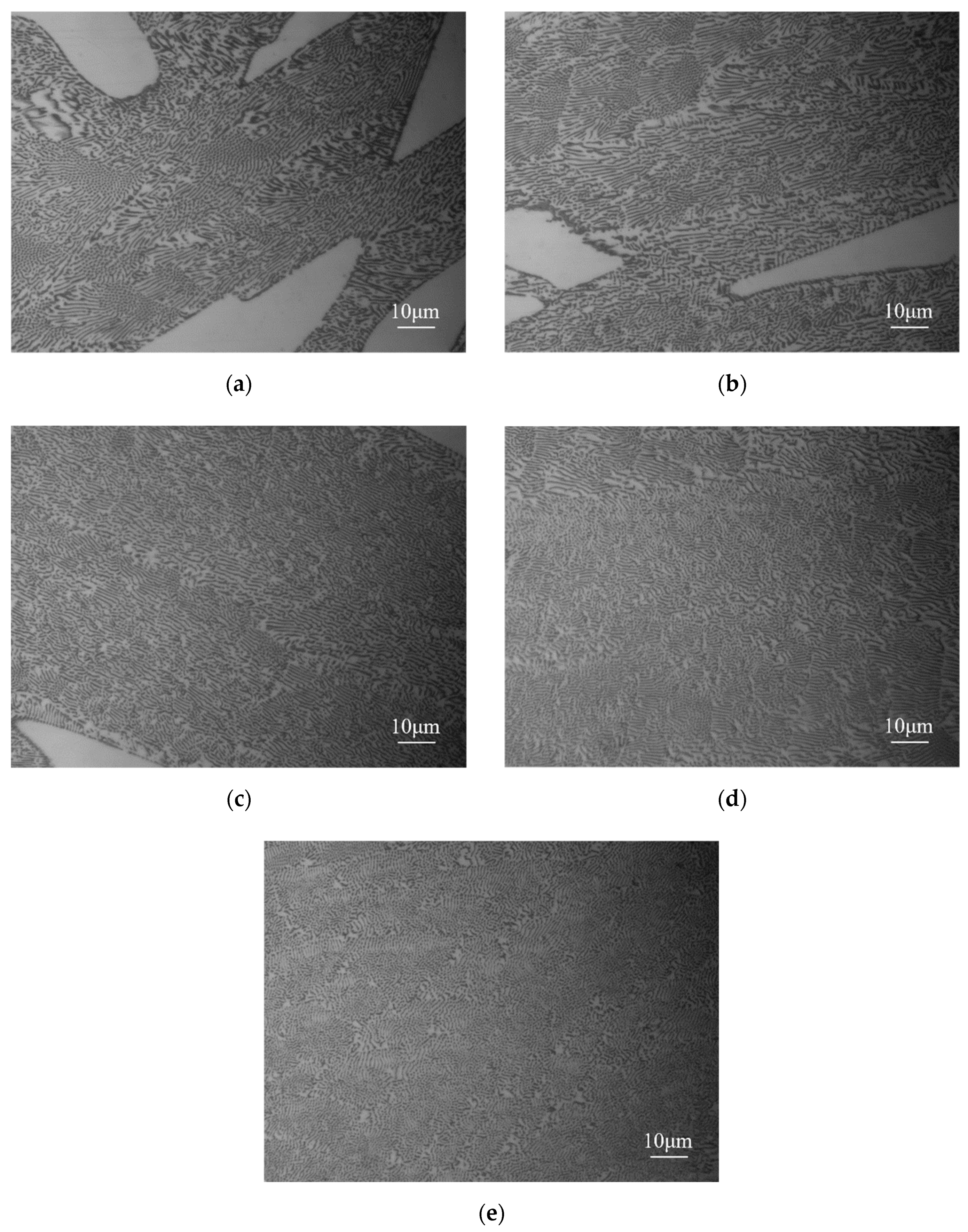
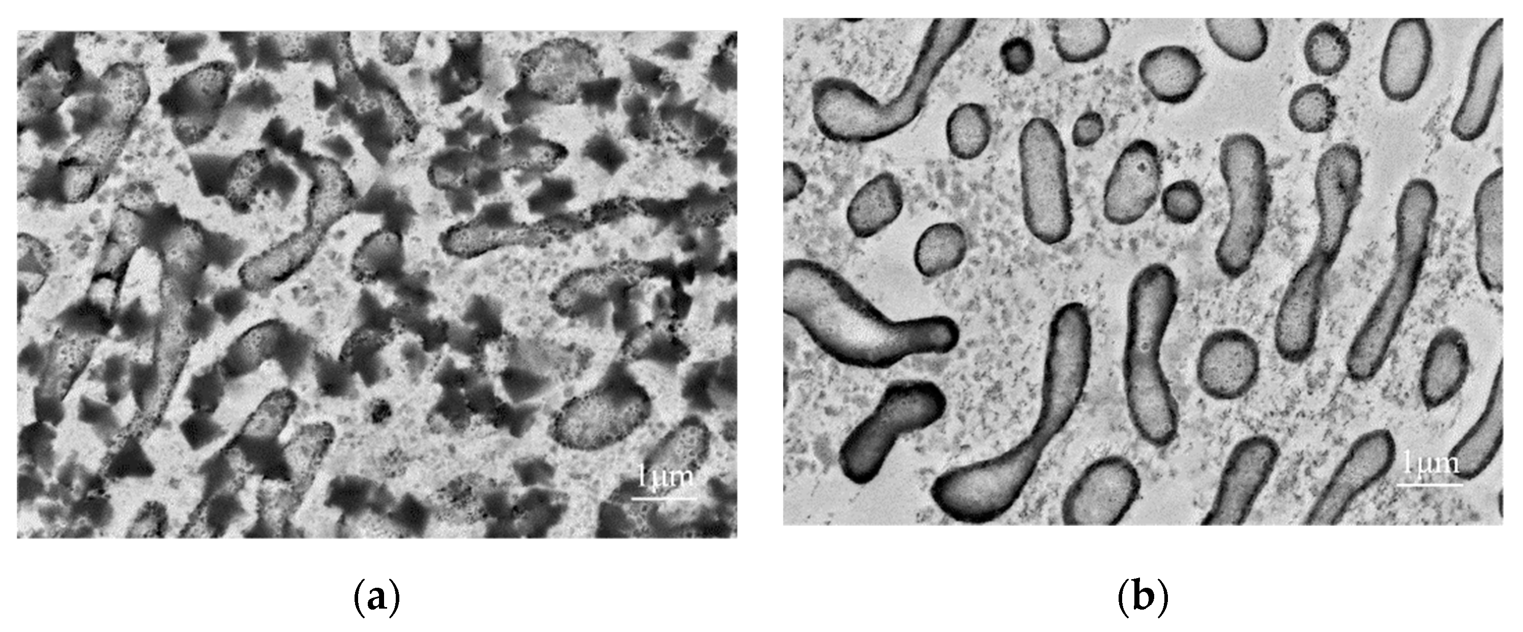
3.1. Effect of Cr on the Matrix Structure of As-Cast Solder

Figure 1 shows the evolution of the as-cast microstructure of AuGa-xCr (x = 0–0.4 wt.%).
The typical structure of AuGa eutectic solder is that fine AuGa2 is evenly distributed on the AuGa substrate. The white phase in the solder matrix is the AuGa phase, and the dark phase is the AuGa2 phase [2]. This conclusion is strongly supported by the EDS results in Table 2. With the addition of Cr, the gray-dark phase structure gradually changed from a lamellar to finer ellipsoid, and at the same time, the large white phase in the solder gradually decreased.
The fineness of the solder microstructure is attributed to the presence of chrome-bearing particles, which play the role of non-uniform nucleation centers [12]. Figure 1a is the as-cast structure of AuGa without Cr doping. It is not difficult to find the existence of a large white phase, which indicates the deviation of the solder composition. According to the phase diagram, the Au-Ga binary phase diagram (Figure 2) [13], the mass fraction of Ga in the solder is lower than the eutectic point; that is, there is a loss of Ga in the smelting process. This is due to the fact that part of the Ga is oxidized to form scum and removed in the smelting process, so the content of Ga in the solder alloy is slightly lower than that in the original composition. With the addition of Cr element, the composition of the solder gradually approaches the eutectic composition, indicating that the loss of Ga element is reduced.
In the process of oxidation on the surface of molten solder, the molecules adsorbed on the molten alloy decompose into oxygen atoms at high temperature and obtain electrons to become negative ions, and finally, oxygen anions combine with metal cations to form oxides [14]. For the system of the multi-element coexistence of solder alloy, the type of oxide formed depends on the Gibbs free energy of each element combining with oxygen. In the AuGaCr solder alloy, the order of the elements in terms of the ability to bind to oxygen is Cr > Ga > Au. Therefore, with the addition of Cr element, Cr is enriched on the surface of the molten solder and oxidizes before the other elements to form a dense oxide film, which effectively blocks the contact between the oxygen in the air and the liquid surface of high-temperature molten solder, thus preventing further oxidation reactions and reducing the loss of Ga.

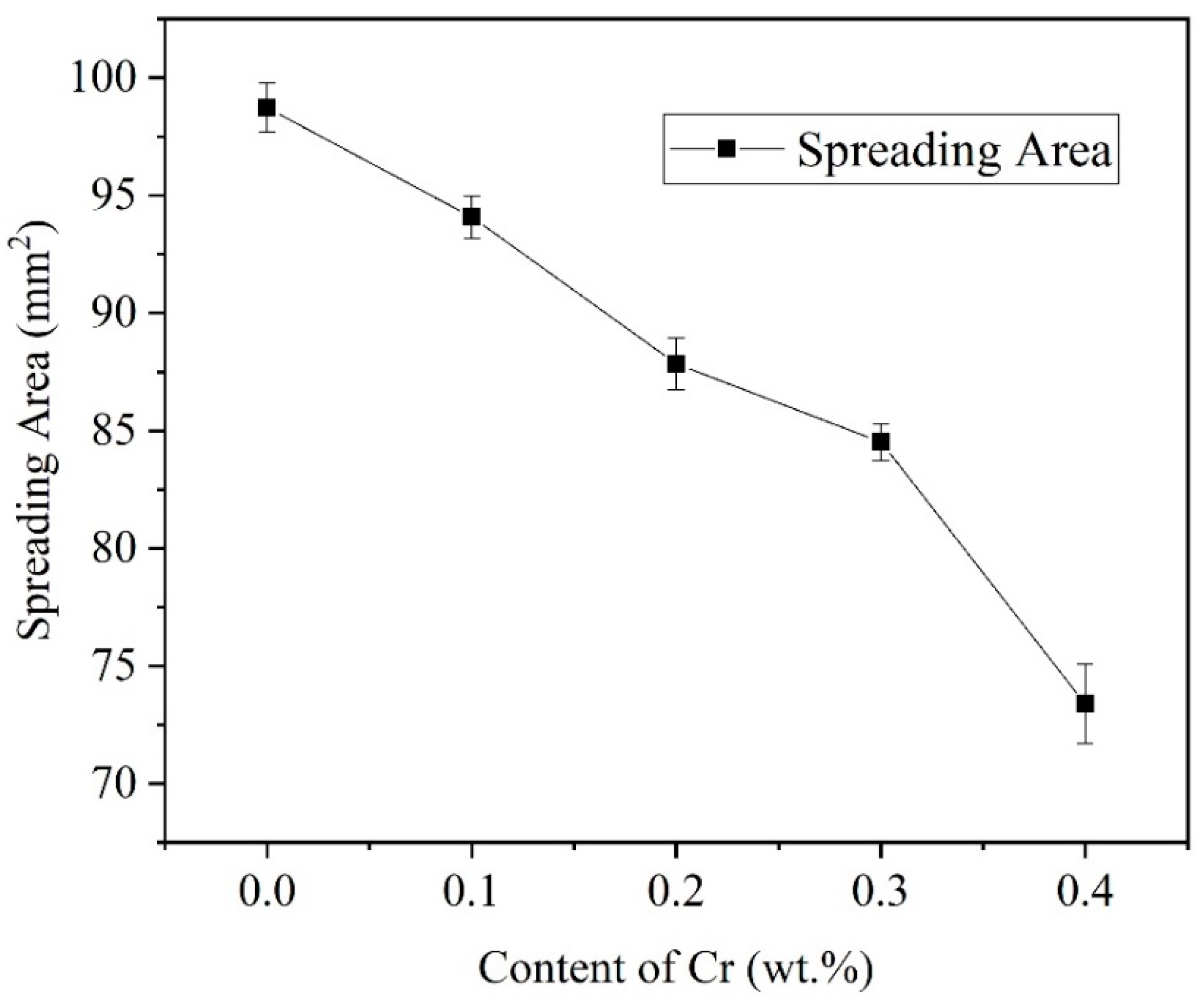
3.2. Effect of Cr Element on Wetting Spreading Performance and Oxidation Resistance of Solder

Figure 3 shows the change in the spreading area of the solder with different contents of Cr. The experimental results show that the spreading area of the solder decreases gradually with an increase in the Cr content. When the addition of Cr element reached 0.4 wt.%, the spreading area of the solder decreased greatly.
The essence of the wetting and spreading of liquid solder on the substrate is that the molten solder diffuses with the substrate through capillarity and infiltrates into the surface of the substrate. This process is shown in Figure 4. Its principle can be expressed by the Young–Dupre formula [15]:
γsv = γls + γlvcosθ
In the formula, γsv, γls and γlv, respectively, represent the surface tensions of the solid–gas, liquid–solid and liquid–gas interfaces during solder spreading and θ is the wetting angle. The wetting process is actually a dynamic process in which the surface tension returns to equilibrium. Since Cr element is concentrated on the solder surface, the oxide generated increases the surface tension of the solder alloy in the molten state, reduces the solder fluidity and leads to a decrease in the spread rate. When the addition of Cr element reached 0.4 wt.%, the spreading area of the solder decreased greatly. When Cr is added in excess, the oxide containing Cr will nucleate, grow up alone and no longer dissolve in the matrix, which greatly increases the surface tension in the process of solder spreading, making the spreading area of the solder decrease greatly [15].
For gold-based solders, such as AuSn solder, excessive flow tends to occur in actual production. As can be seen in Figure 3, the spreading area of 50 mg of AuGa solder reaches 98.2 mm2. This value means that AuGa solder has excellent wetting and spreading properties on a Ni substrate. At the same time, it also means that in the practical application process, the excessive use of solder or the problem of a slightly higher temperature may lead to the excessive diffusion and irregular overflow of solder, which will affect the normal use of electronic devices. When adding 0.3 wt.% Cr, the wetting spreading area of the solder decreases to 84.5 mm2, but it still meets the requirements of application. Therefore, the addition of an appropriate amount of Cr element has positive significance, which prevents the excessive overflow of solder on the basis of ensuring excellent wetting and spreading properties.
In order to further analyze the surface morphology of the solder and the oxidation condition after aging, and explore the effect of Cr on enhancing the oxidation resistance of the solder, scanning electron analysis was carried out on AuGa and AuGa-0.3Cr spreading samples after oxidation at 300 °C for 240 h, as shown in Figure 5.
It can be seen from Figure 5 that there are many large black phases in the oxide layer on the surface of AuGa solder, with a size of 0.5 μm. By contrast, the AuGa-0.3Cr surface is relatively smooth and dense, without a large black phase, which indicates that a uniform protective film is formed on the surface of the solder to prevent further oxidation of the solder. The EDS analysis in Region A shows that the surface oxygen content of AuGa solder is high, up to 12.2 wt.%. The composition of the black phase is shown in Table 3. The atomic ratio of Ga to O is about 2:3, and the phase is presumed to be Ga2O3. By comparison, the surface oxygen content of Cr-containing solder is low, which indicates that the existence of an oxide film enhances the oxidation resistance of the solder. At the same time, the EDS analysis in Region B shows that the Cr content on the surface of AuGa-0.3Cr solder is 1.27 wt.%, which is higher than that in the solder. This phenomenon is due to the surface enrichment effect of Cr element, which tends to accumulate on the surface or sub-surface of the solder and is oxidized to form a protective layer [16,17].

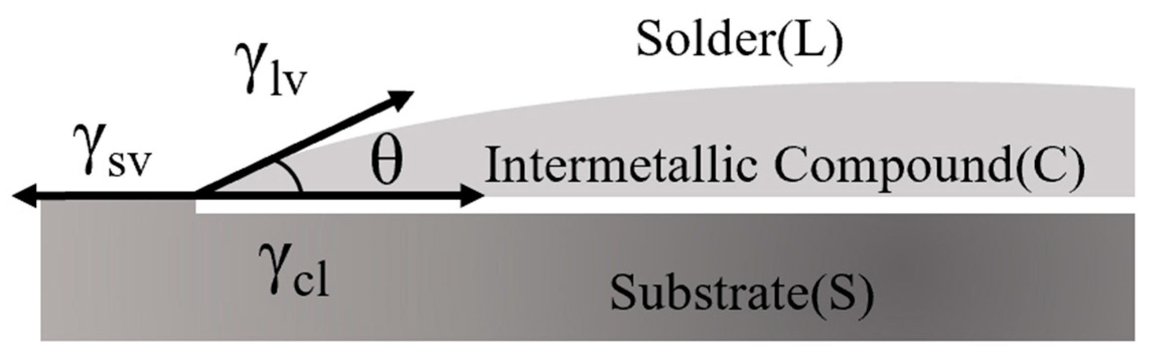
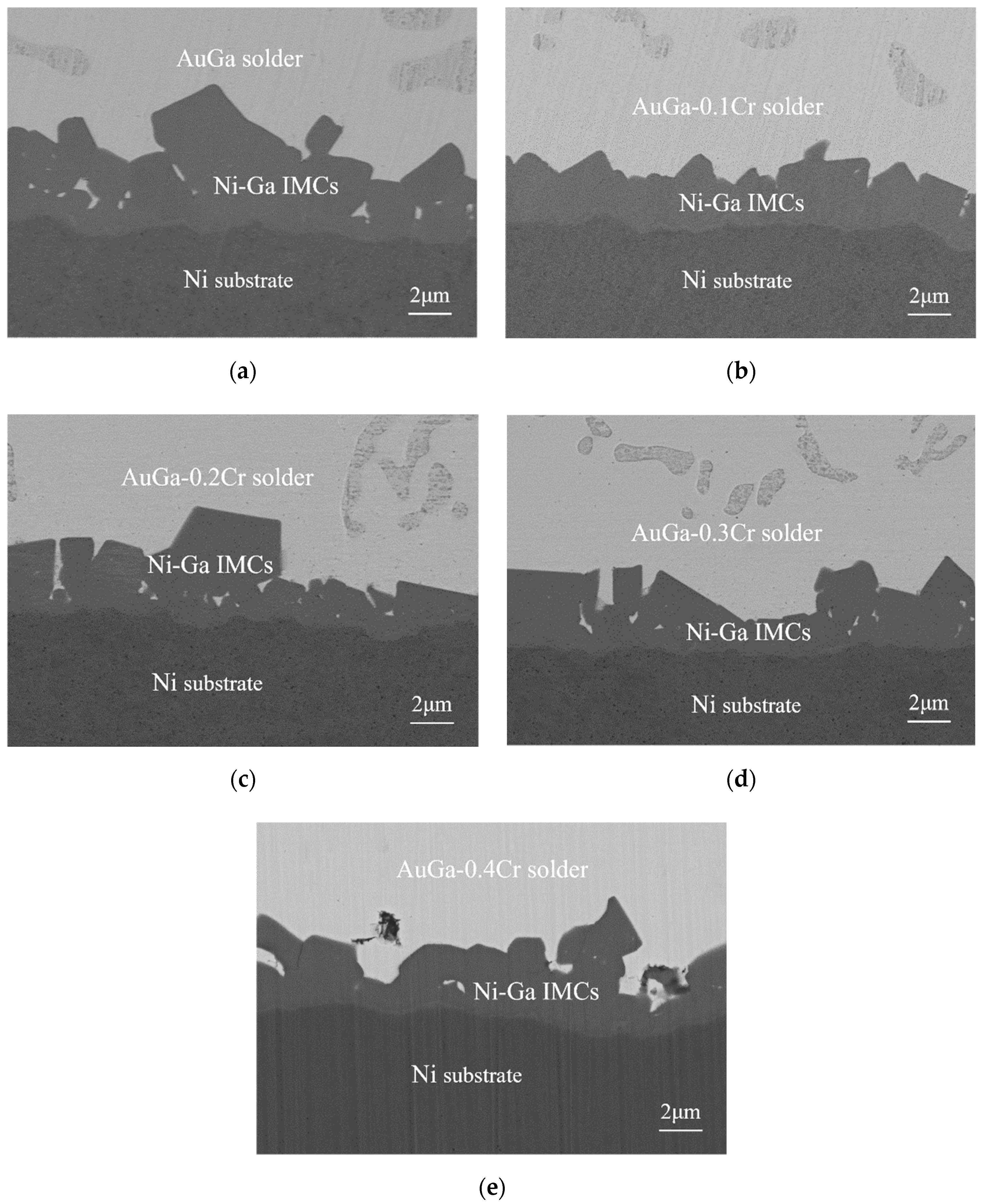
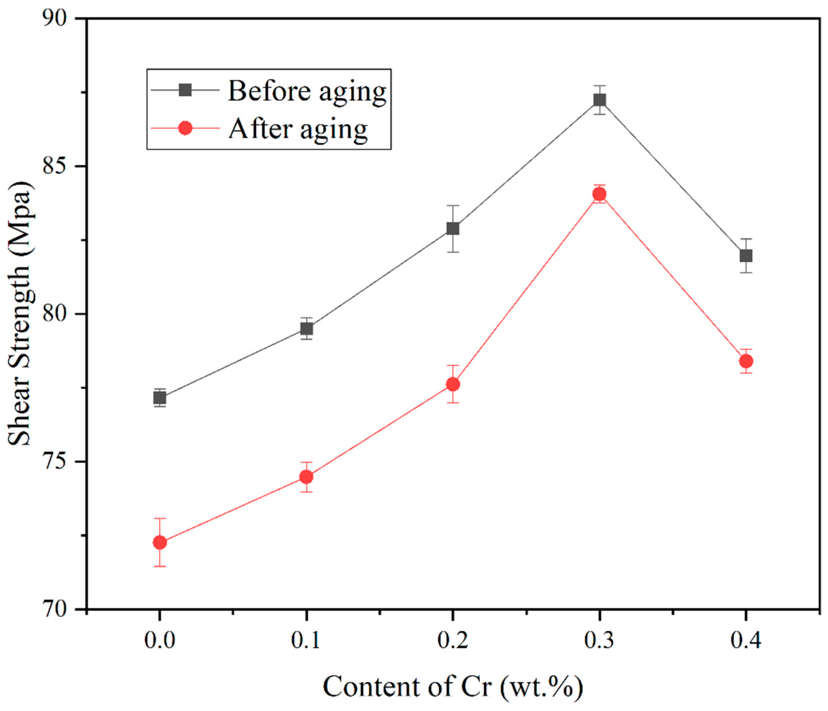
3.3. Effect of Cr Element on Microstructure and Mechanical Properties of Joint Interface

Several studies [18,19] have shown that the high diffusibility and rapid reaction of lead-free solders, as well as increasingly small chip sizes, have led to the formation of a large number of intermetallic compounds (IMCs) in solder joints. With increases in the aging time, deformation velocity and IMC layer thickness, the ductile failure mode of the whole solder changed to the brittle failure mode for the IMC layer. Lee et al. [19,20] proposed that the mechanical properties of solder joints mainly depend on the performance of the IMCs, which indicates that the interface morphology plays a very important role in the mechanical properties of welded joints. Thus, it is necessary to study the influence of Cr on the evolution of welded interfaces. Figure 6 shows the microstructure at the interface between the AuGa-xCr (x = 0, 0.1, 0.2, 0.3, 0.4) solder and the Ni substrate.
It can be seen that two layers of Ni-Ga compound layer were formed at the interface between the Ni substrate and solder. The composition analysis shows that the interface layer on the solder side was Ni2Ga3, while the interface layer with a small thickness on the substrate side is β phase [2,21]. The AuGa/Ni interface compound layer presents a uniform and continuous shape in small pieces. With the addition of Cr, the morphology of the interface layer remained unchanged, and the thickness of the interface layer decreased slightly. When the content of Cr reached 0.4 wt.%, due to the existence of bulk oxide, defects such as holes could be observed at the interface of the solder, which is consistent with the results of the wetting spreading experiment. The results show that the addition amount of the Cr element should not be excessive, otherwise it will have an adverse effect on the soldering performance of the solder. The best addition amount is 0.3 wt.%.
Figure 7 shows the changes in the mechanical properties of the AuGa-xCr/Ni solder joints. It can be seen that before and after aging, the addition of Cr had a significant enhancement effect on the mechanical properties of the AuGa solder joints. Before aging, when the content of Cr was lower than 0.3 wt.%, the mechanical properties of the solder joints showed an upward trend with an increase in Cr content. The shear strength of the AuGa-0.3Cr joint was 87.2 MPa, which is 13.1% higher than that of the AuGa joint. On the one hand, this is due to the optimization of the joint interface morphology; on the other hand, the presence of Cr-containing particles plays a reinforcing role, as they act as the second-phase particles and hinder grain boundary slip and dislocation movement [22]. When the Cr content was further increased to 0.4 wt.%, the mechanical properties of the joint decreased due to the existence of defects at the interface. After aging at 300 °C for 240 h, the mechanical properties of the joint showed a similar trend. The shear strength of the AuGa-0.3Cr joint was still the peak value, which is 16.3% higher than that of the AuGa solder joint. The experimental results show that the addition of Cr element can effectively improve the mechanical reliability of solder under high-temperature service conditions.

4. Conclusions

In this work, the effects of Cr addition on the as-cast microstructure, wettability, surface oxidation and mechanical properties of AuGa solder were studied. The results show that:
(1)
The addition of 0.3 wt.% Cr reduced the loss of Ga element in the process of smelting and casting, and effectively improved the uneven composition of the as-cast microstructure of the solder matrix.
(2)
Although the spreading area of the solder decreased slightly after adding a trace amount of Cr, it still met the requirements for application and prevented the excessive overflow of solder. Cr was enriched on the surface of the solder and oxidized to form a dense and stable protective film, which enhanced the oxidation resistance of the solder.
(3)
The addition of 0.3 wt.% Cr optimized the interface morphology and improved the mechanical properties of the solder joint. The shear strength of the solder joint reached 87.2 MPa, which was 13.1% higher than that of the solder joint without Cr element. After aging at 300 °C for 240 h, the shear strength of the AuGa-0.3Cr joint was still the peak value at 84.1 MPa, which was 16.3% higher than that of the AuGa joint.

Author Contributions

Methodology, Y.T.; software, Y.T.; investigation, Y.T. and H.L., writing—original draft preparation, Y.T.; writing—review and editing, S.X., Y.T. and B.W.; supervision, S.X.; project administration, S.X. and W.L.; funding acquisition, S.X. All authors have read and agreed to the published version of the manuscript.

Funding

This project was supported by the National Natural Science Foundation of China (Grant No. 51675269); the State Key Laboratory of Advanced Brazing Filler Metals & Technology (Zhengzhou Research Institute of Mechanical Engineering Co., Ltd.), China (Grant No. SKLABFMT201704); and the Priority Academic Program Development of Jiangsu Higher Education Institutions (PAPD).

Conflicts of Interest

The authors declare no conflict of interest.

References

  1. Ramli, M.I.I.; Saud, N.; Salleh, M.A.A.M.; Derman, M.N.; Said, R.M. Effect of TiO2 additions on Sn-0.7Cu-0.05Ni lead-free composite solder. Microelectron. Reliab. 2016, 65, 255–264. [Google Scholar] [CrossRef]
  2. Liu, H.; Xue, S.; Tao, Y.; Long, W.; Zhong, S. Design and solderability characterization of novel Au–30Ga solder for high-temperature packaging. J. Mater. Sci. Mater. Electron. 2020, 31, 2514–2522. [Google Scholar] [CrossRef]
  3. Chidambaram, V.; Yeung, H.B.; Shan, G. High reliability gold based solder alloys for micro-electronics packaging for high temperature applications. In Proceedings of the 19th IEEE International Symposium on the Physical and Failure Analysis of Integrated Circuits, Singapore, 2–6 July 2012. [Google Scholar]
  4. Zhao, H.; Liu, J.; Li, Z.; Song, X.; Zhao, Y.; Niu, H.; Tian, H.; Dong, H.; Feng, J. A Comparative Study on the Microstructure and Mechanical Properties of Cu6Sn5 and Cu3Sn Joints Formed by TLP Soldering With/Without the Assistance of Ultrasonic Waves. Metall. Mater. Trans. A 2018, 49, 2739–2749. [Google Scholar] [CrossRef]
  5. Chin, H.S.; Cheong, K.Y.; Ismail, A.B. A review on die attach materials for SiC-based high-temperature power devices. Metall. Mater. Trans. B 2010, 41, 824–832. [Google Scholar] [CrossRef]
  6. Xiong, M.; Zhang, L.; Sun, L.; He, P.; Long, W. Effect of CuZnAl particles addition on microstructure of Cu/Sn58Bi/Cu TLP bonding solder joints. Vacuum 2019, 167, 301–306. [Google Scholar] [CrossRef]
  7. Zhu, W.; Zhang, W.; Zhou, W.; Wu, P. Improved microstructure and mechanical properties for SnBi solder alloy by addition of Cr powders. J. Alloys Compd. 2019, 789, 805–813. [Google Scholar] [CrossRef]
  8. Bi, J.; Hu, A.; Hu, J.; Luo, T.; Li, M.; Mao, D. Effect of Cr additions on interfacial reaction between the Sn–Zn–Bi solder and Cu/electroplated Ni substrates. Microelectron. Reliab. 2011, 51, 636–641. [Google Scholar] [CrossRef]
  9. Chen, X.; Hu, A.; Li, M.; Mao, D. Effect of a trace of Cr on intermetallic compound layer for tin–zinc lead-free solder joint during aging. J. Alloys Compd. 2009, 470, 429–433. [Google Scholar] [CrossRef]
  10. Chen, X.; Li, M.; Ren, X.; Hu, A.; Mao, D. Effect of small additions of alloying elements on the properties of Sn-Zn eutectic alloy. J. Electron. Mater. 2006, 35, 1734–1739. [Google Scholar] [CrossRef]
  11. Chen, X.; Hu, A.; Li, M.; Mao, D. Study on the properties of Sn–9Zn–xCr lead-free solder. J. Alloys Compd. 2008, 460, 478–484. [Google Scholar] [CrossRef]
  12. Liu, M.; Yang, W.; Ma, Y.; Tang, C.; Tang, H.; Zhan, Y. The electrochemical corrosion behavior of Pb–free Sn–8.5Zn–xCr solders in 3.5 wt.% NaCl solution. Mater. Chem. Phys. 2015, 168, 27–34. [Google Scholar] [CrossRef]
  13. Okamoto, H. Au-Ga (Gold-Gallium). J. Phase Equilib. Diffus. 2013, 34, 174–175. [Google Scholar] [CrossRef]
  14. Gan, G.; Du, C.; Luo, Y.; Chen, F.; Yang, B. Effect of Trace Ni, Al and Cr on the Surface Film Structure of Sn-Pb Liquid Alloys. Adv. Mat. Res. 2011, 217–218, 969–975. [Google Scholar]
  15. Zhang, S.; Zhu, B.; Zhou, X.; Wang, X.; Lin, T.; He, P.; Paik, K.W. Wettability and interfacial morphology of Sn–3.0 Ag–0.5 Cu solder on electroless nickel plated ZnS transparent ceramic. J. Mater. Sci. Mater. Electron. 2019, 30, 17972–17985. [Google Scholar] [CrossRef]
  16. Zhang, L.; Xue, S.; Gao, L.; Sheng, Z.; Ye, H.; Xiao, Z.; Zeng, G.; Chen, Y.; Yu, S. Development of Sn–Zn lead-free solders bearing alloying elements. J. Mater. Sci. Mater. Electron. 2010, 21, 1–15. [Google Scholar] [CrossRef]
  17. Luo, T.; Hu, A.; Hu, J.; Li, M.; Mao, D. Microstructure and mechanical properties of Sn–Zn–Bi–Cr lead-free solder. Microelectron. Reliab. 2012, 52, 585–588. [Google Scholar] [CrossRef]
  18. Tu, K.N.; Liu, Y. Recent advances on kinetic analysis of solder joint reactions in 3D IC packaging technology. Mater. Sci. Eng. 2019, 136, 1–12. [Google Scholar] [CrossRef]
  19. Annuar, S.; Mahmoodian, R.; Hamdi, M.; Tu, K.N. Intermetallic compounds in 3D integrated circuits technology: A brief review. Sci. Technol. Adv. Mater. 2017, 18, 693–703. [Google Scholar] [CrossRef] [PubMed] [Green Version]
  20. Lee, C.; Hsieh, C.; Guo, Y.; Lin, Y.; Zhan, C.; Chang, T. Reliability enhancement of ultra-thin chip assembly module in 3D-ICs integrations by the assistance of molding compounds. In Proceedings of the Microsystems, Packaging, Assembly & Circuits Technology Conference, Taiwan, China, 22–24 October 2014. [Google Scholar]
  21. Liu, H.; Xue, S.; Tao, Y.; Long, W.; Zhong, S.; Wang, B. Wetting behavior and vacuum soldering of novel Au-30Ga solder on Ni and Cu substrate. Vacuum 2020, 179, 109478. [Google Scholar] [CrossRef]
  22. Zhang, P.; Xue, S.; Wang, J.; Xue, P.; Long, W. Effect of Nanoparticles Addition on the Microstructure and Properties of Lead-Free Solders: A Review. Appl. Sci. 2019, 9, 2044. [Google Scholar] [CrossRef] [Green Version]
Figure 1. The as-cast microstructure of AuGa-xCr: (a) AuGa; (b) AuGa-0.1Cr; (c) AuGa-0.2Cr; (d) AuGa-0.3Cr; (e) AuGa-0.4Cr.
Metals 10 01449 g001
Figure 2. Au-Ga phase diagram [13].
Metals 10 01449 g002
Figure 3. Spreading area of AuGa-xCr (x = 0, 0.1, 0.2, 0.3, 0.4).
Metals 10 01449 g003
Figure 4. Schematic diagram of the wetting process.
Metals 10 01449 g004
Figure 5. Surface microstructure of AuGa and AuGa-0.3Cr solder: (a) AuGa; (b) AuGa-0.3Cr.
Metals 10 01449 g005
Figure 6. Interface microstructure of AuGa-xCr/Ni: (a) AuGa; (b) AuGa-0.1Cr; (c) AuGa-0.2Cr; (d) AuGa-0.3Cr; (e) AuGa-0.4Cr.
Metals 10 01449 g006
Figure 7. Shear strength of AuGa-xCr/Ni solder joint before and after aging (x = 0, 0.1, 0.2, 0.3, 0.4).
Metals 10 01449 g007
Table 1. Chemical composition of solder alloys (wt.%).
No.AuGaCr
1Bal.300
2Bal.300.1
3Bal.300.2
4Bal.300.3
5Bal.300.4
Table 2. EDS analysis of two phases in microstructure.
PhaseAu (at.%)Ga (at.%)
the white phase54.7545.25
the dark phase34.3065.70
Table 3. EDS analysis of black phase.
Elementswt.%at.%
Ga43.9533.38
O16.0653.15
Au35.709.06
Ni4.293.87
Publisher’s Note: MDPI stays neutral with regard to jurisdictional claims in published maps and institutional affiliations.

