Article

Influence of Deposition Temperature on the Structure and Current-Carrying Friction Performance of Cu Films by DC Magnetron Sputtering Technology

1
School of Materials Science and Engineering, China University of Petroleum (East China), Qingdao 266580, China
2
State Key Laboratory of Solid Lubrication, Lanzhou Institute of Chemical Physics, Chinese Academy of Sciences, Lanzhou 730000, China
3
School of Mechanical & Automotive Engineering, Qingdao University of Technology, Qingdao 266033, China
4
Shandong Laboratory of Yantai Advanced Materials and Green Manufacturing, Yantai 264000, China
5
Yantai Zhongke Research Institute of Advanced Materials and Green Chemical Engineering, Yantai 264000, China
6
Key Laboratory of Solidification Processing, Northwestern Polytechnical University, Xi’an 710072, China
*
Authors to whom correspondence should be addressed.
Lubricants 2023, 11(1), 8; https://doi.org/10.3390/lubricants11010008
Submission received: 24 November 2022 / Revised: 20 December 2022 / Accepted: 21 December 2022 / Published: 26 December 2022
(This article belongs to the Special Issue Friction and Wear of Coatings/Films)

Abstract

:
The structure and morphology of Cu films deposited by DC magnetron sputtering on silicon and stainless-steel substrates at different deposition temperatures of −140 °C, −95 °C, −55 °C, 25 °C (RT), 50 °C, and 200 °C were investigated by X-ray diffraction (XRD), scanning electron microscopy (SEM), and atomic force microscopy (AFM). It was found that all Cu films presented strong orientation of the (111) and (200) peaks. The Cu films deposited at low temperatures (lower than −55 °C) showed the bilayer structures, in which the upper layer appeared to be a loose and porous structure and the lower layer near the substrate had a fine and dense structure that consisted of small grains. In addition, the Cu films deposited at low temperatures could be observed a large roughness. The roughness tended to decline and then increase with the rising of deposition temperature. The ball-on-disc reciprocating sliding tribometer was employed to evaluate the tribological behaviors of the Cu films at current-carrying levels of 0 A, 0.5 A, and 1.0 A. The results revealed that the Cu films deposited at low temperatures exhibited outstanding current-carrying friction performance and low electrical contact resistance (ECR), peeling only at 0.5 A and 1.0 A. Nevertheless, the Cu films deposited at the relatively high temperature exhibited oxidative wear caused by electric arc ablation at 0.5 A and 1.0 A. Additionally, the wear mechanism was discussed in terms of the structure and morphology of the wear track and formation of the tribo-film.

1. Introduction

According to the relevant data, about 20% of primary energy production is needed to overcome friction forces, and 60% of the failure of moving components has been due to severe wear [1,2]. The economic loss caused by friction and wear has been as high as hundreds of billions every year. The simple and the most common way to reduce friction and wear has been to use lubricants between interacting rolling or sliding surfaces to reduce solid–solid contact. The solid lubricant coatings could be applied under heavy load, low pressure, high temperatures, high speed, high risk of contamination, and other extreme conditions in which the liquid lubricants are ineffective [3,4,5]. Therefore, the application prospects of solid lubricant coatings to reduce friction and wear were promising [6,7] and some related studies have focused on them [8,9,10]. Nevertheless, the applications of some solid lubricant coatings (oxides, polymers, sulfides) were inadvisable in some special situations such as micro–nano electromechanical systems in current-carrying conditions.
Copper, a non-noble metal, has been widely used in industry due to its prominent electrical conductivity close to that of noble metals such as silver and gold. Thus, it is regarded as the most ideal and promising conductive material for microelectronics and electrical contact components, especially for electronic connections of high-speed integrated circuits with sub-micron characteristics [11,12,13]. Moreover, because of the low shear strength and excellent tribological property of Cu, the deposited Cu film has a crucial role in the lubrication of tribo-components in micro–nano electromechanical systems. The Cu film has emerged as an inexpensive alternative to the noble metals of Ag and Au for the lubrication of precision components.
Extensive efforts have been dedicated to developing a Cu film with high performance via electron beam evaporation [14], physical and chemical vapor depositions [15,16], electroplating [17], chemical plating [18], and ion beam sputtering [19]. Among them, the magnetron sputtering technology has been more and more extensively employed to fabricate film materials because it can possess high purity, homogeneity, and controllable accuracy of film thickness [20,21]. For example, M. Geetha deposited Cu films by DC magnetron sputtering and studied the electrical properties of Cu films. The results showed that Cu films have high electrical conductivity [15]. In addition, Cao indicated that Cu films deposited by DC magnetron sputtering appeared to have a good anti-wear mechanism due to the fine crystal strengthening produced by the friction [22]. In this regard, the construction of a Cu film with a well-defined nanostructure was critical for achieving excellent friction behavior and anti-wear performance. Importantly, with the aid of the beneficial plasma atmosphere controlled by the process parameters (Ar pressure, deposition temperature, and the substrate bias voltage) in the magnetron sputtering, the microstructure of the Cu film can be tailored, ultimately achieving high tribological performance [23,24,25]. Notably, the deposition temperature of film for preparing the excellent microstructure and the correspondingly improved properties had been reported [16,26]. For instance, the Ti70Al30 film deposited at low temperatures had a much denser structure compared with the film prepared at room temperature [27]. The (110) orientation of the Fe film deposited at low temperatures was improved remarkably compared to that of the room temperature-deposited film [28]. Weng et al. reported that the Ag film deposited at low temperature by arc ion plating exhibited higher wear resistance [16]. However, as the inexpensive alternatives to the Ag and Au films, the tribological properties and electrical conductivity of the Cu films deposited by DC magnetron sputtering technology at low temperatures have been rarely reported.
Bearing the perspectives in mind and viewing the few reports, and to further enhance the tribological performance of the sputtering Cu film, a variety of structures of Cu film have been fabricated by using the DC magnetron sputtering method in this study. The microstructure, morphology, mechanical/tribological properties, and wear mechanisms of those films were systematically investigated and compared. Altering the optimal deposition temperature of Cu films was certified to be an effective approach for tailoring its current-carrying friction and wear behaviors.

2. Experimental Details

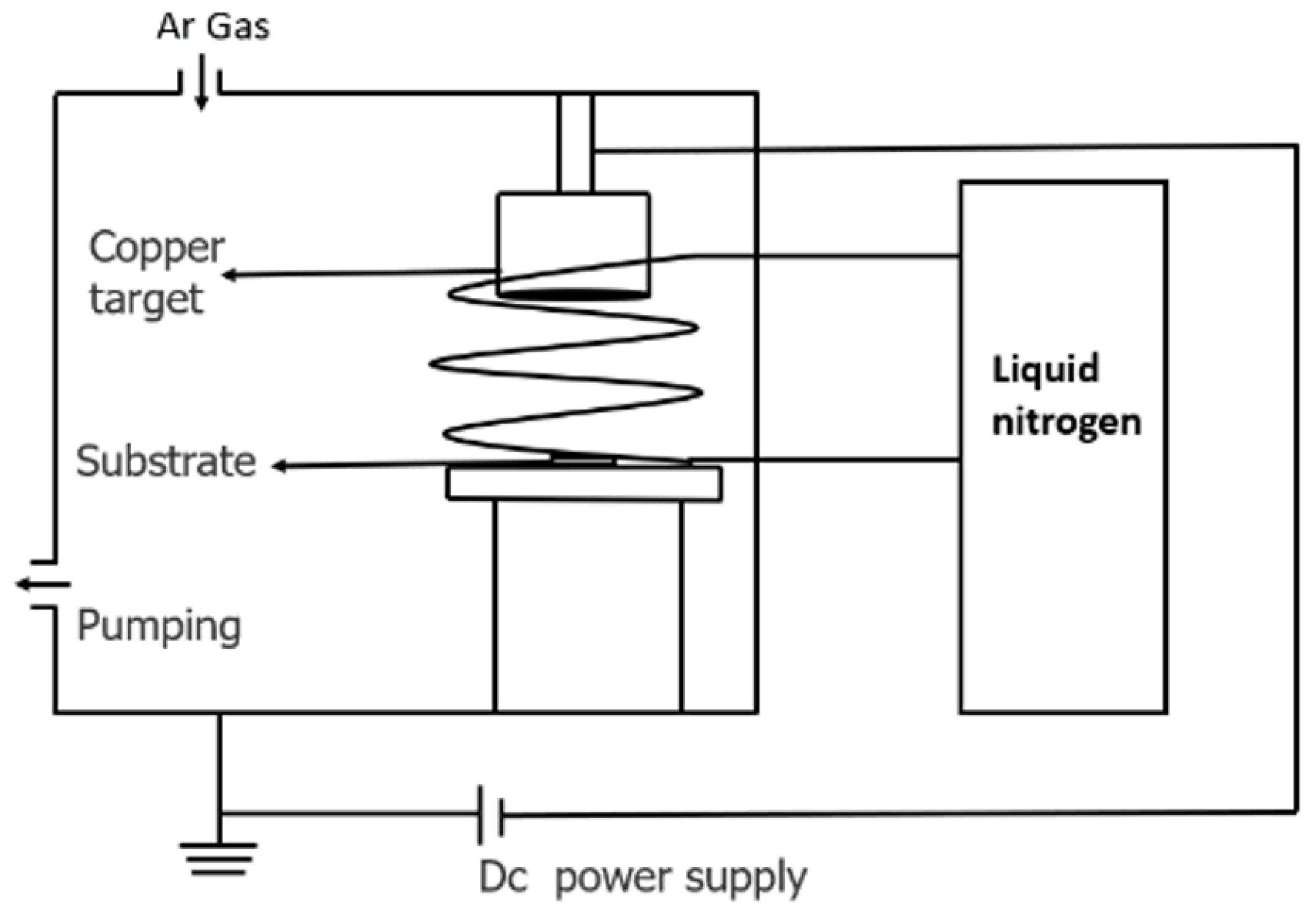
2.1. Film Deposition

The deposition system of Cu films is illustrated in Figure 1. The copper target was regarded as the DC cathode with a purity of 99.95%, 76.2 mm in diameter and 4 mm in thickness. The surface between the Cu target and substrates was parallel to each other, and the Cu target was approximately 60 mm far away from the substrates. The geometry of the 304 stainless-steel (SS) substrates were quadrate with dimensions of 20 mm × 20 mm × 2 mm, of which the Cu films were selected for the analysis of current-carrying friction and wear behavior, while the films on the silicon substrates were used to investigate the morphology. Prior to deposition, the substrates were ultrasonically cleaned with petroleum ether and alcohol for 10 min, respectively, and then blown dry. In general, the Cu film on the SS and Si wafer surface without an interlayer was easily exfoliating due to the poor adhesion between Cu films and substrates. Therefore, it was essential to deposit the Ti buffer layer on the substrates that enhances the adhesion between the Cu films and the substrates. Typical deposition conditions for the Ti buffer layer are illustrated in Table 1.
The high purity argon gas (99.999%) was used to deposit Cu films by DC magnetron sputtering. Before the deposition, the chamber was pumped to a standard pressure of 5 × 10⁻³ Pa. In order to eliminate possible pollutants on the surface, the Ti buffer layer needed to be etched by Ar ion. The deposition pressure in the chamber was kept at 0.3 Pa during this film growth and the deposition time was 5 min. To study the effect of substrate temperatures on the tribological performance and conductive capacity of Cu film, a series of Cu films were deposited at −140 °C, −95 °C, −55 °C, RT, 50 °C, and 200 °C, and the deposition temperatures were measured by a Platinum thermocouple attached to the surface of the substrate. The detailed DC deposition parameters are listed in Table 2.

2.2. Film Characterization

The crystallographic structures of Cu films were characterized by X-ray diffraction (XRD) operating at 40 kV using Cu Ka radiation, in which the diffraction patterns were obtained by stepwise scanning in the range of 20° and 80° with a scan rate of 5° min−1. The morphology and cross-sectional microstructures of Cu films were observed by field-emission scanning electron microscopy (FESEM). The surface roughness (Rq) of the films was investigated by the multimode atomic force microscope (AFM). After the sliding test, the wear tracks were observed using scanning electron microscopy (SEM) and an optical microscope. The elements in the wear tracks were analyzed by energy dispersive spectroscopy (EDS).

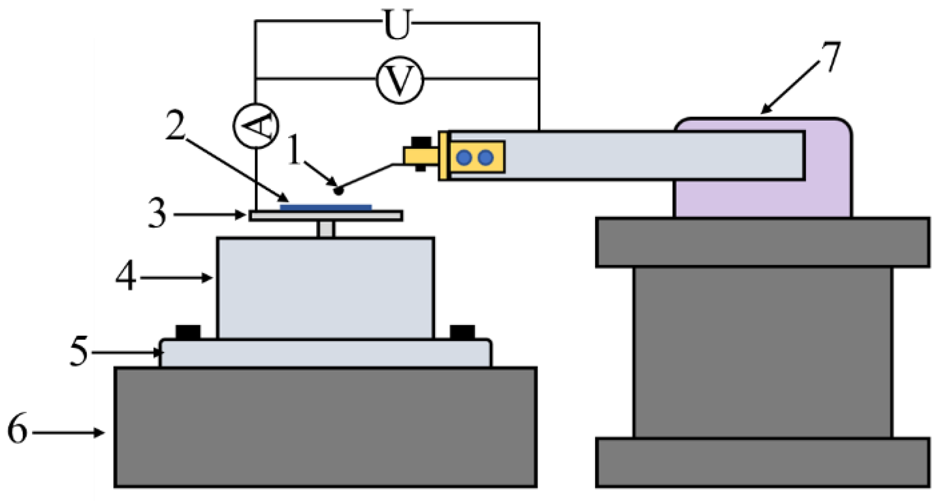
2.3. Tribological Properties Test

The ball-on-disc reciprocating sliding tribometer was used to test the tribological behaviors of the Cu films deposited at different temperatures with and without current. The 440C SS balls with diameters of 3.2 mm were used as the corresponding tribo-pairs. The electrical currents of 0.5 A or 1 A were supplied by the direct-current power station. Figure 2 displays the device diagram of test equipment for the current-carrying friction test. The current flows from the positive pole of the power supply to the bottom of the SS plate and then returns to the negative pole via the 440C SS ball. Tribological tests were carried out in the atmospheric environment with a normal load of 0.1 N, sliding frequency of 4 Hz, and reciprocating amplitude of 4 mm.

3. Results and Discussion

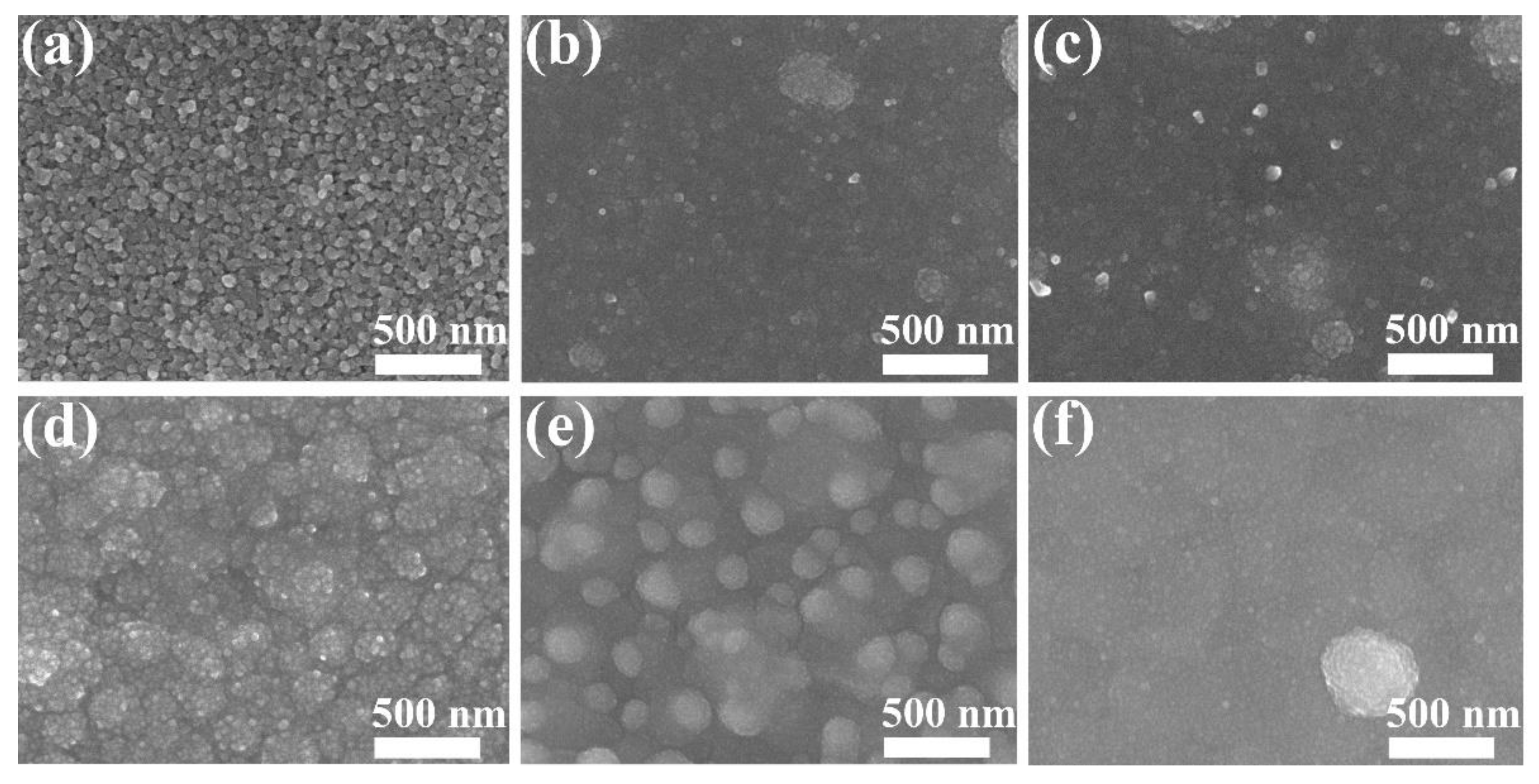
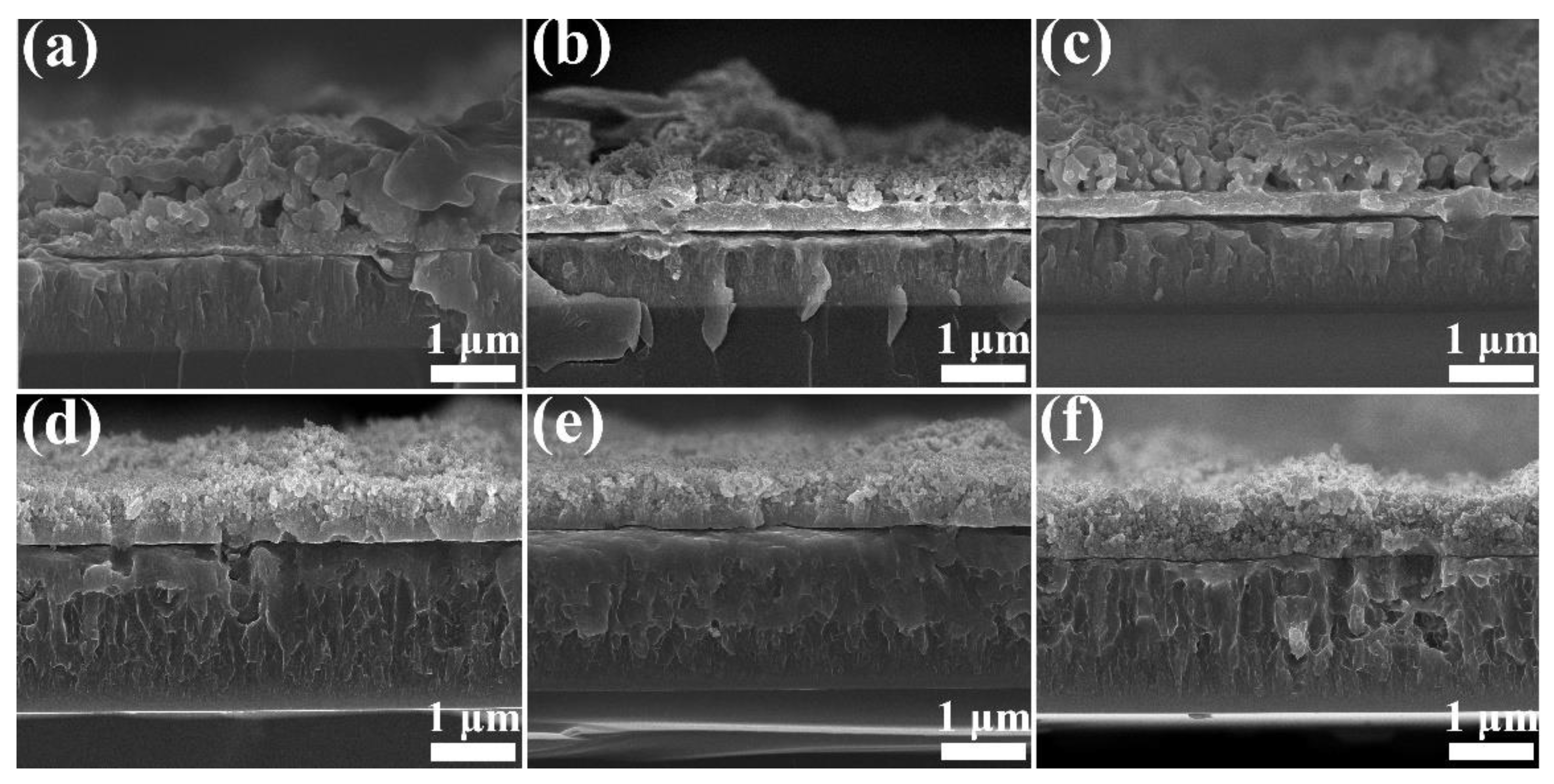
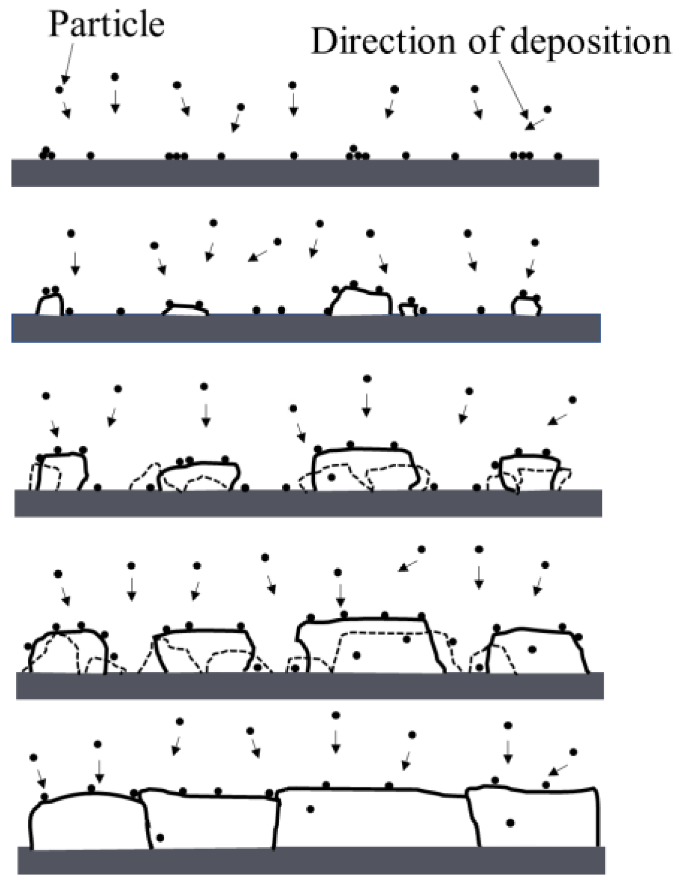
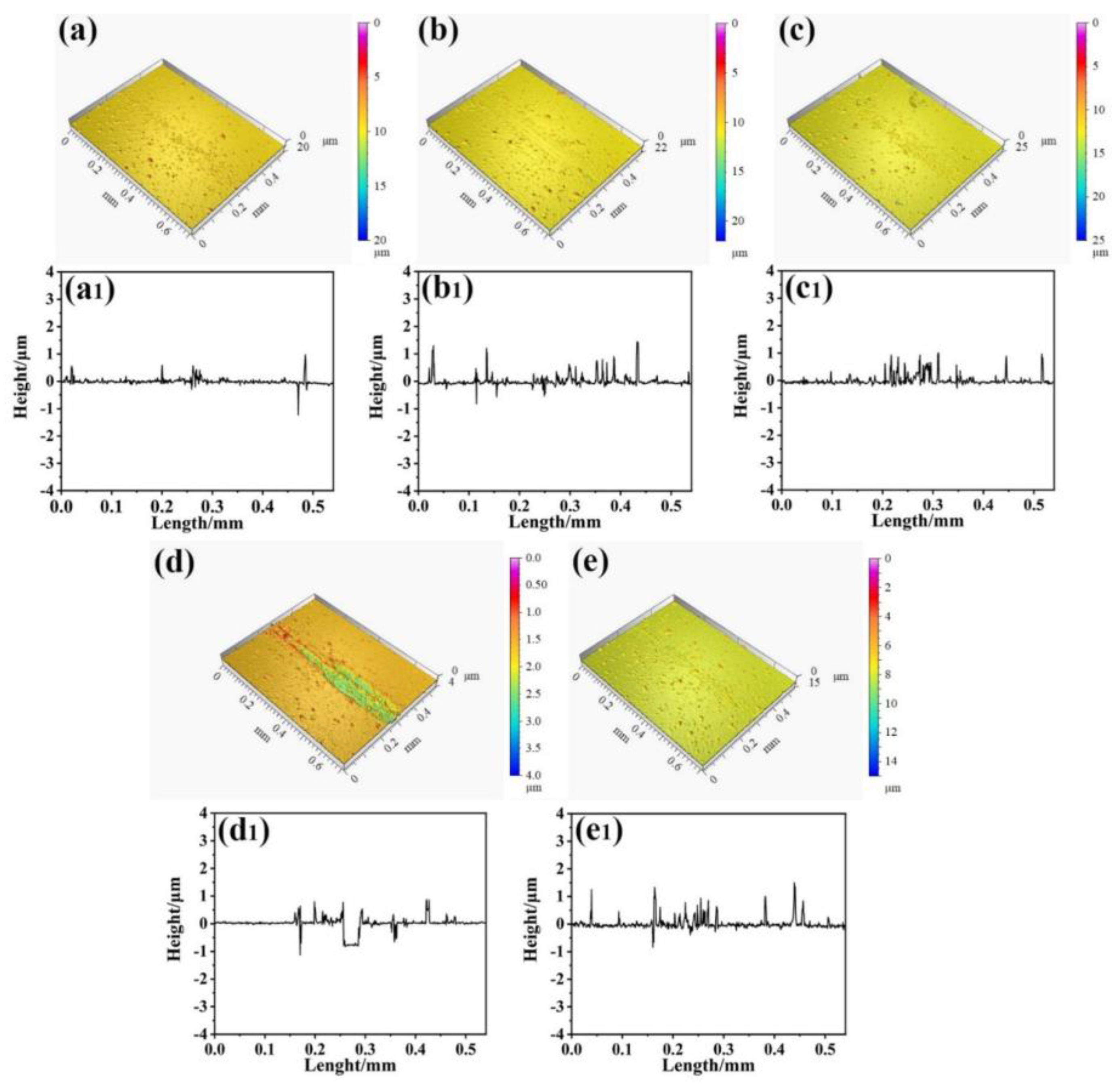
3.1. Structure of Film

Figure 3 exhibits the grazing incidence X-ray diffraction (GIXRD) spectra of Cu films deposited on SS substrates at different temperatures from −140 °C to 200 °C. It can be seen that except for the diffraction peaks of the Ti interlayer, all the Cu films showed the fcc-Cu (111), (200), and (220) peaks with a preferred orientation of the (111) plane, even though they were deposited at different temperature atmospheres. Furthermore, there was no strict linear relationship between crystallinity and temperature. As the deposition temperature gradually decreased from 50 °C and RT to −140 °C, the Cu (111) peak first became sharper and then broadened, and as it increased to 200 °C, the Cu (111) peak also turned sharper, indicating that both the crystallinity and grain size decreased in the range of 50 °C and RT as well as −140 °C. These results were not consistent with the trend of crystallinity increasing with the temperatures, suggesting the difference in the structure of Cu films deposited at various temperatures. As reported, the crystal grain always grew in the plane direction of the lowest energy of the crystal plane [29,30]. Thus, the film possessed significant (111) and (200) planes corresponding to the low surface energy and strain energy crystal planes of the fcc-Cu crystal [31].
The surface morphologies of the various Cu films were investigated by AFM and the images are shown in Figure 4, which presents the typical 3D AFM micrograph characteristics of the structure and grain of Cu films at various deposition temperatures varying from −140 °C to 200 °C in the scan size of 50 × 50 μm2. All the films exhibited the coarse grain feature, with the typical grain characteristics of Cu films deposited at low temperatures becoming prominent. Figure 4g presents the surface roughness Rq of Cu films versus the deposition temperature. It can be found that the Rq value declines gradually from 0.439 μm to 0.280 μm as the deposition temperature increases from −140 °C to 50 °C. The high deposition temperature led to a further increase in roughness Rq to 0.27 μm. This suggested that the temperature of 50 °C can be a critical deposition temperature in this study, at which the deposited ions might possess the high diffusion rate to form the relatively small grain as well as the low surface roughness. Zhang et al. used the kinetic Monte Carlo technique to simulate the growth of Cu films [32]. They pointed out that the film deposited at the transition temperature had the minimum surface roughness. Overall, the deposition temperature atmosphere played a vital role in the crystal grain growth of Cu films.
The SEM images of surface morphologies of the Cu films are shown in Figure 5. It can be found that the temperature had an obvious influence on the surface morphology of the Cu films [33,34]. The surface of the film deposited at −140 °C showed a loose structure consisting of polygon-like grains. The −95 °C Cu and −55 °C Cu films displayed the similar intact surface morphology and a small number of rough clusters composed of fine grains. As the deposition temperature increased to RT, the Cu film was characterized by numerous single clusters, which mainly grew in the vertical direction, forming the structure morphology with “V” shape. This was because the nucleation density on the substrate was lower, leading to the vertical crystals growing much faster than other directions [35]. With the further increase in the deposition temperature to 50 °C, the film surface rough clusters gradually disappeared and evolved into an intact structure composed of large grains. Furthermore, the clusters tended to merge, and the uniform compact structure was formed, which was much denser than the films deposited at low temperatures. This can be attributed to the high mobility and surface diffusion of adatoms in the high temperature atmosphere. According to Equations (1) and (2), the growth of grain is related to surface diffusion and increases exponentially with temperature.
v = v 0 e x p ( Δ E K B T )
D n D 0 n = K ( T ) t
where v is the surface diffusion rate, v0 is the frequency of atom vibration [v0 = 2 K B T h ], D is the average grain diameter, D0 is the initial grain diameter, n is the grain growth exponent, K(T) is the grain growth constant [K(T)∝exp ( Δ E K B T )], h is the Plank constant, ΔE is the activation energy, KB is the Boltzmann constant, T is the temperature, and t is time.
Because the substrate was heated at the high temperature, the adatoms could gain extra energy apart from the energy generated by the impact of energetic target atoms when they reached the film surface during the deposition process [36,37]. This leads to the considerable surface diffusion of the energetic adatoms, enabling the adatoms to migrate a long distance and occupy lattice sites maintaining energy stability [38,39,40], which is in favor of the grain growth and leads to a stronger structure.
To obtain details of film structure, in addition to SEM images of the surface morphology of the Cu films, we further characterized the cross-sectional structure of the Cu films, and the SEM images are shown in Figure 6. All the Cu films deposited at the low temperature in the range of −140 °C to −55 °C had a bilayer structure, in which the upper layer possessed a loose and porous structure and the lower layer close to the substrate presented a fine and dense structure consisting of small grains. As reported, the upper loose structure always presented large crystal grains with the preferred growth while the dominant component of the dense lower layer consisted of tiny grains or even an amorphous phase, resulting from the low migration of adatoms during the growth process at the low temperatures [41,42,43]. With the increase of deposition temperatures in the range of RT to 200 °C, the upper layer turned into a dense structure without any layer delamination or the appearance of bilayer characterization, and the grains became much finer than the films deposited at low temperatures. To some extent, the dense cross-section comprised columnar platelets. Therefore, the grain orientation and intensity of the diffraction peaks are heavily affected by the structures of Cu films, which can be observed in Figure 3. As for the bilayer Cu films (−140 °C, −95 °C, and −55 °C), the peaks’ intensity increased with the deposition temperatures, suggesting the increase of the crystallinity of the films. In addition, the single-layer Cu films (RT, 50 °C, and 200 °C) showed the same trend. Thus, in this work, due to the different structures of Cu films deposited at various temperatures, there is no strict linear relationship between the crystallinity and the temperature. However, there is a clear linear relationship between crystallinity and temperature for the same-structure Cu films.
Generally, the growth processes of the microstructural evolution of deposited films consisted of five stages: (1) nucleation, (2) island growth, (3) impingement and coalescence of islands, (4) formation of polycrystalline islands and channels, and (5) development of a continuous structure, and the illustration is shown in Figure 7 [44]. Apparently, the mobility and surface diffusion of the atoms have a significant effect on each step during deposition [27,45]. In the initial growth stage of film, the low-temperature atmosphere prevents the mobility and surface diffusion of the adatoms as well as the formation of a critical nucleus for further crystal growth, resulting in the relatively low crystallinity of the lower layer close to the substrate surface. As each single grain island grows up, they bond with each other at the grain boundaries, and consequently, the continuous structure of the film can be formed in the lower layer. In the second growth stage, both the mutual blocking effect and shadow effect of adjacent grains can facilitate the grains to grow vertically at the boundaries because of the freer geometric space in the vertical direction. Thus, the loose, porous, and anisotropic structure was obtained in this deposition stage. In comparison, the Cu film deposited at a relatively high-temperature atmosphere can uniformly grow and finally form a dense structure with a relatively smooth surface. This was because the mobility and surface diffusion of adatoms were enhanced in the energetic atmosphere, and thus the gaps among the grains could be filled by the incident atoms [46].

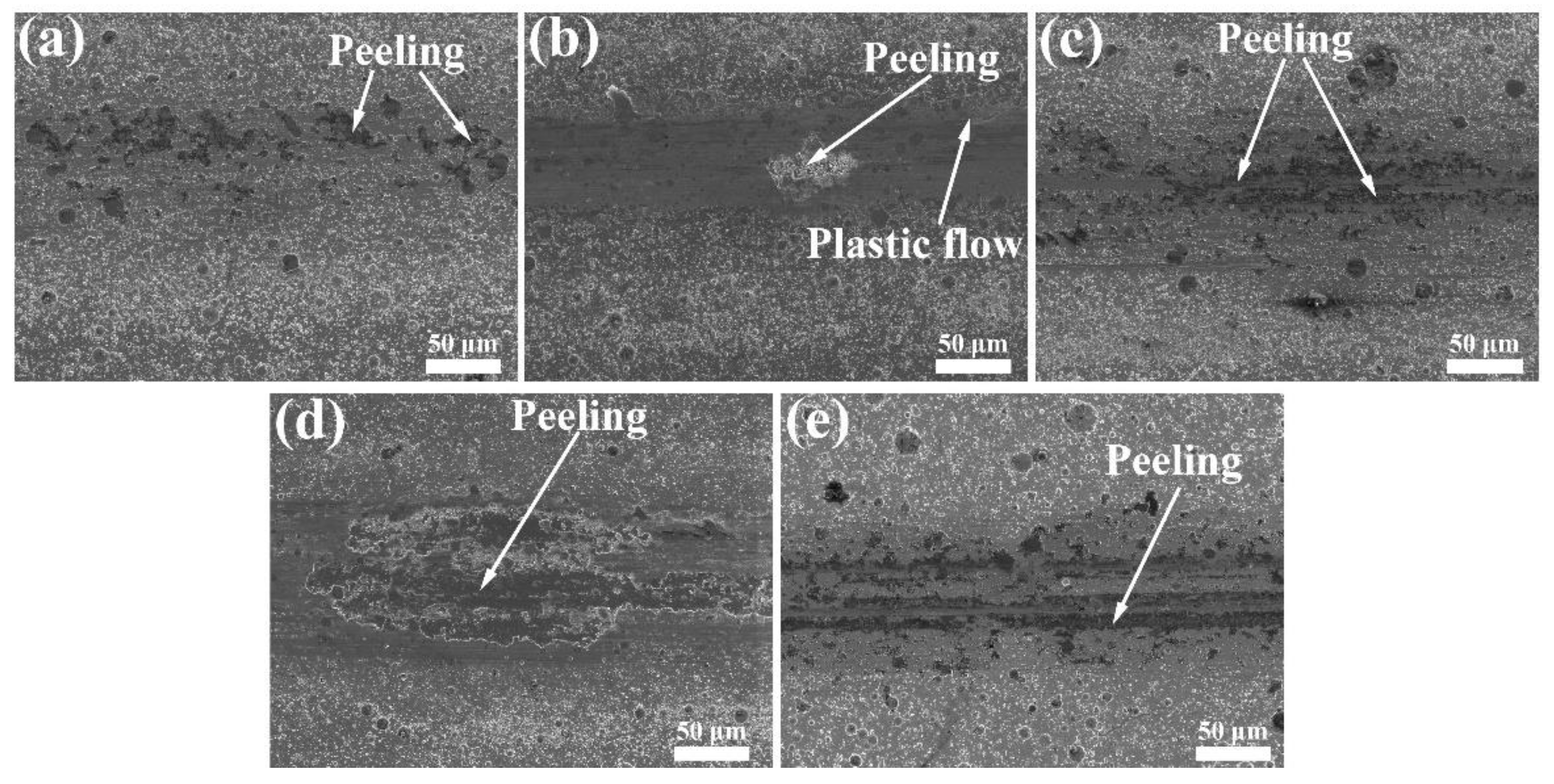
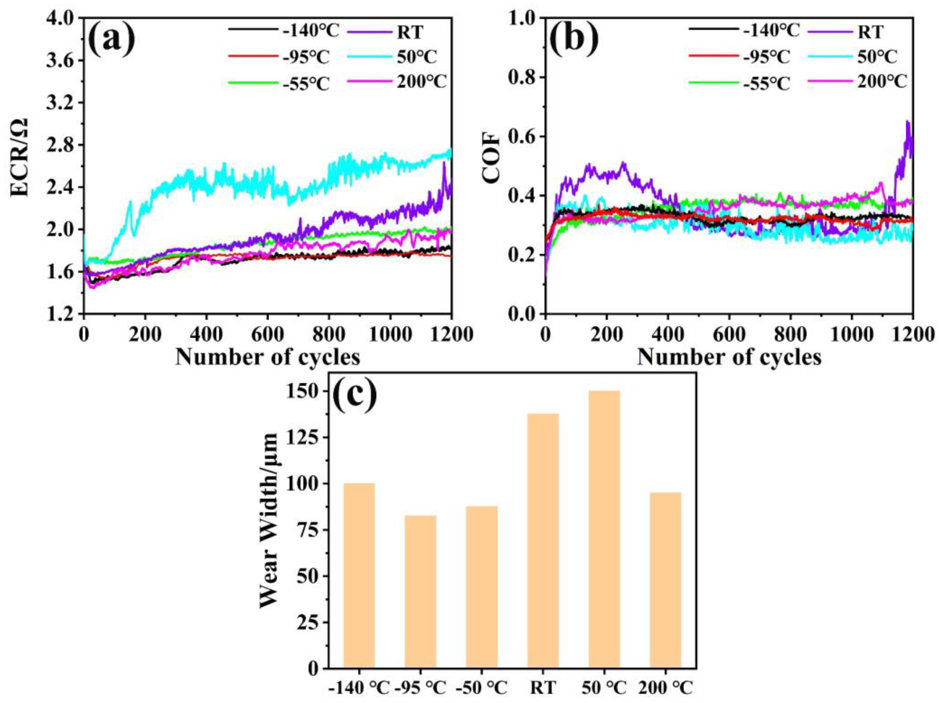
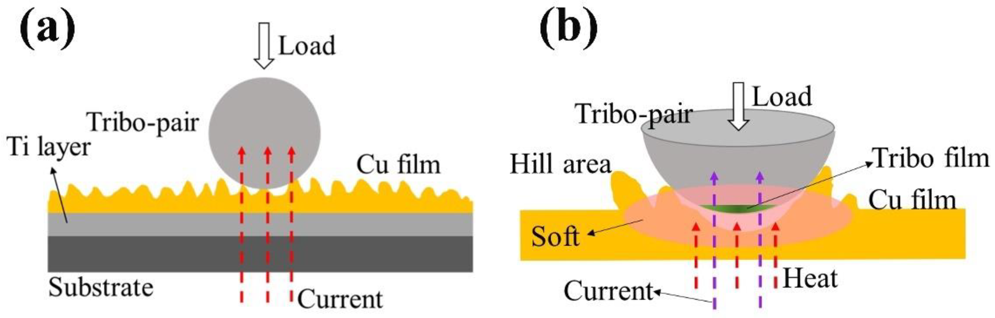
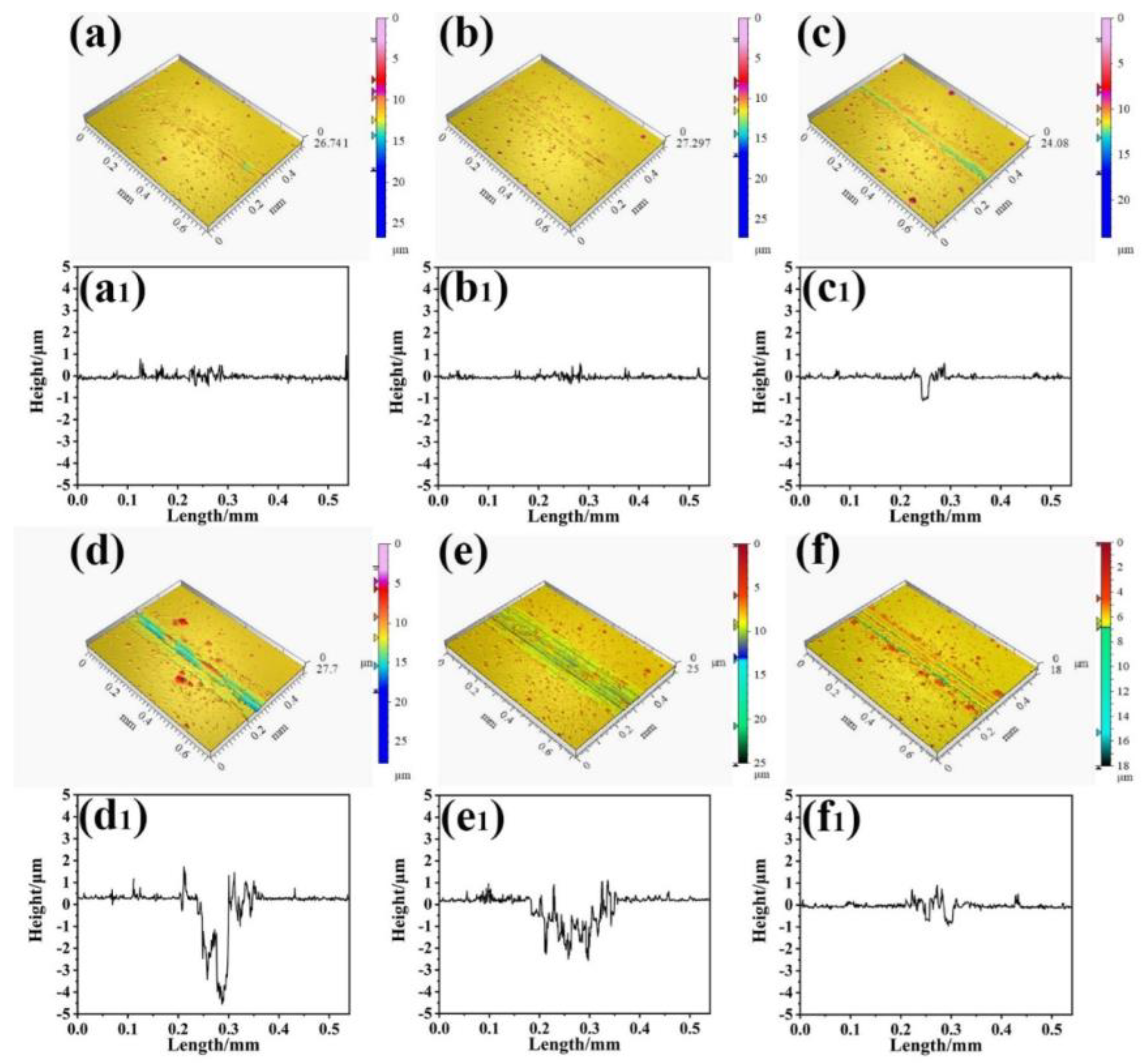
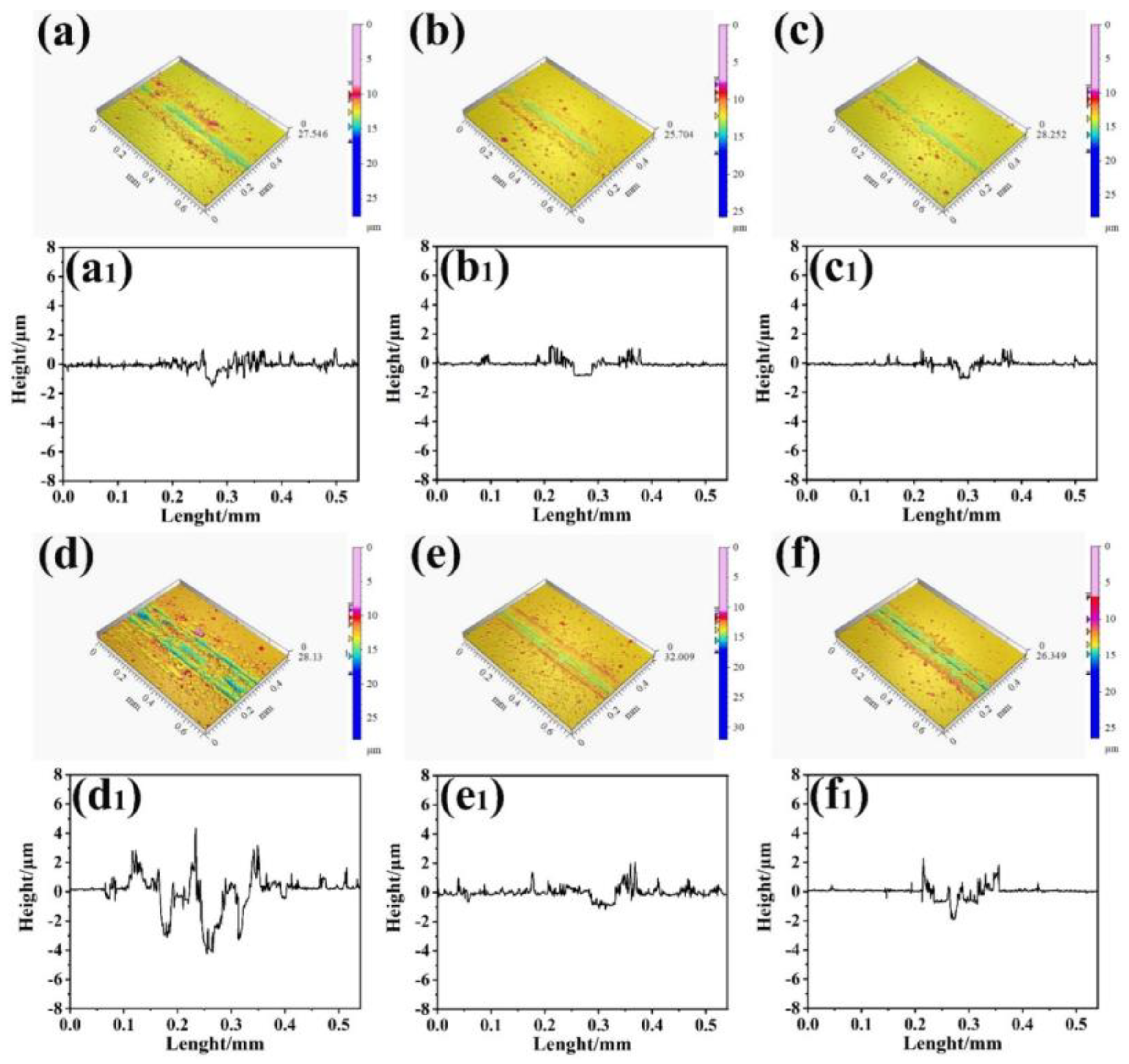
3.2. Tribological Properties

3.2.1. Tribological Performance without Electric Current

The reciprocating sliding test was used to evaluate the friction and wear behaviors of the Cu films deposited at different temperatures. The evolutions of the coefficient of friction for 1200 and 8000 cycles without the electric current are presented in Figure 8. It can be found that in the initial sliding of 1200 cycles, the friction coefficients of Cu films deposited at low temperatures (−140 °C, −95 °C, and −55 °C), 50 °C and 200 °C were approximately ~0.25, 0.28, and 0.3, respectively, as shown in Figure 8a. In comparison, the Cu film deposited at RT presented a relatively high coefficient of friction, which tended to increase gradually during the friction process, and it went up to 0.6 after rubbing 1200 cycles, suggesting the lubrication failure. This indicates that, except for the one deposited at RT, there are not dramatic distinctions in the coefficients of friction for Cu films in the initial sliding stage. All the coefficients of friction of Cu films gradually went up with further sliding, in which the values reached up to 0.40, 0.33, 0.45, 0.47, and 0.50 for the films deposited at −140 °C, −95 °C, −55 °C, 50 °C, and 200 °C, respectively, as shown in Figure 8b. Obviously, the Cu film deposited at −95 °C possessed the lowest coefficient of friction, while the 200 °C-Cu film had the highest coefficient of friction.
To further evaluate the tribological performance of the Cu films, the wear tracks after sliding tests of 8000 cycles were investigated. The 3D images and the corresponding cross-section profiles of the wear tracks of the Cu films are shown in Figure 9. The wear tracks of the Cu film deposited at the low temperatures of −140 °C, −90 °C, and −55 °C were almost invisible, as shown in Figure 9(a–c,a1,b1,c1). The Cu film deposited at 50 °C, as shown in Figure 9(d,d1), exhibited severe wear with a high-depth track. In comparison, the −55 °C Cu and 200 °C Cu presented obvious fluctuation, especially in the cross-section profiles, as shown in Figure 9(c1,e1). The differences in 3D images and the corresponding cross-sectional profiles of the wear tracks of Cu films imply that the Cu films deposited at different temperatures have different wear mechanisms.
In order to further explore the wear characteristics of the Cu films, the wear tracks of Cu films were investigated after the sliding of 8000 cycles. Figure 10 shows the SEM images of the wear tracks of the Cu films. Except for the relatively smooth wear track of the Cu film deposited at −95 °C, many pad-like wear debris were observed on the wear tracks of the films deposited at −140 °C and −55 °C, and severe peeling was also formed on the wear tracks of films deposited at 50 °C and 200 °C. On the basis of the structure analysis and performance evaluation results of the Cu films deposited at different temperatures, it was confirmed that the structure of the −95 °C-Cu film is beneficial to improve tribological performances under the non-electric current conditions. Compared with other deposition temperatures, the scratch surface of the −95 °C-Cu was smoother, and there was an evident plastic flow on the scratch track, which could explain the reason that the Cu film deposited at −95 °C took on the lowest friction coefficient.

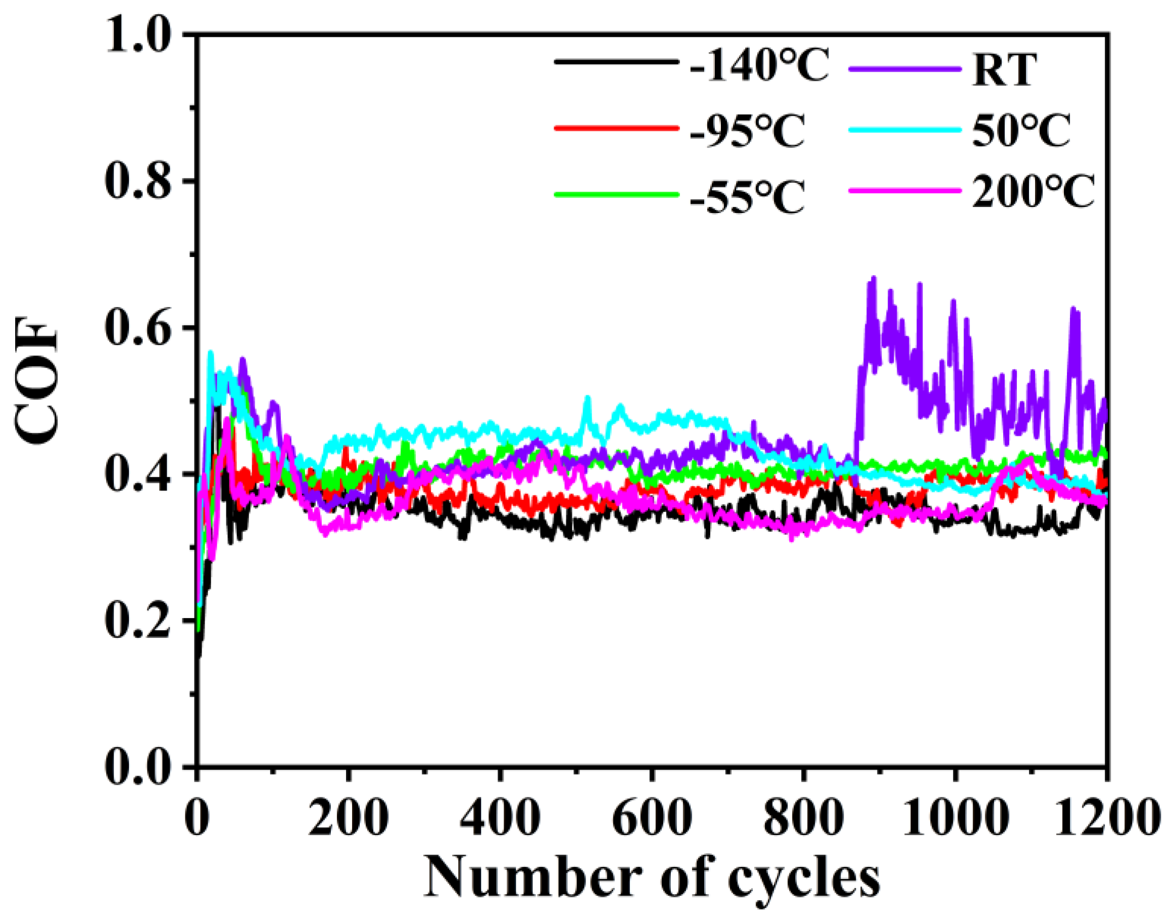
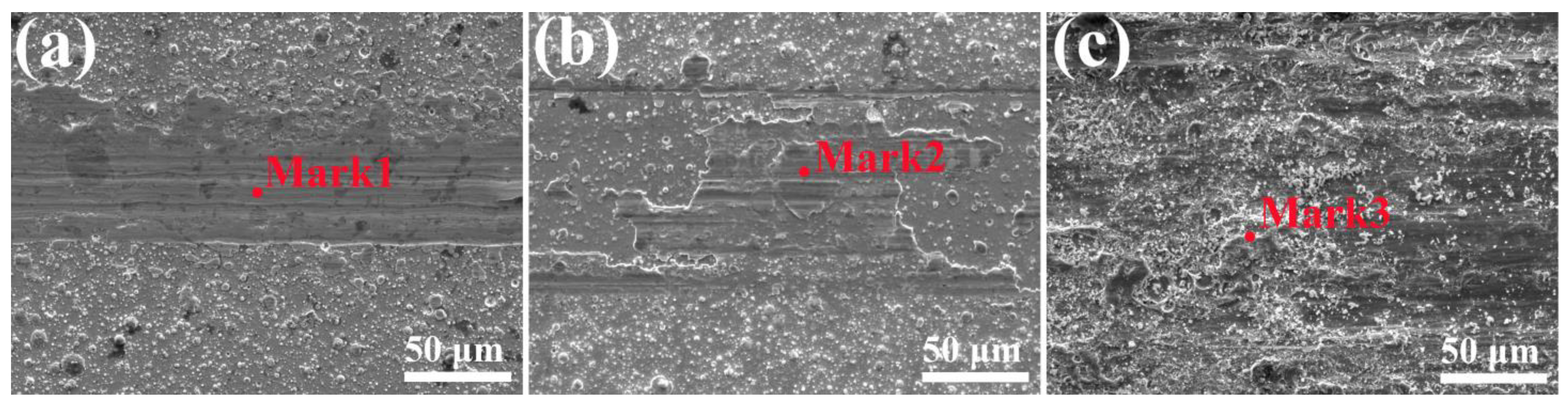
3.2.2. Tribological Performance with Electric Current

Figure 11 gives the ECR and coefficient of friction curves of Cu films deposited at different temperatures as a function of the number of sliding cycles at the electric current of 0.5 A. The ECR curves for the films deposited in the range of −55 °C to 200 °C increase gradually with the rising of sliding cycles, especially for the film deposited at RT and 50 °C; the ECR values reached up to 2.3 Ω and 2.7 Ω, respectively, after rubbing 1200 cycles. In comparison, the ECR values for the films deposited at −140 °C to −95 °C kept almost unchanged during the sliding of 1200 cycles, which was in the range of 1.5~1.7 Ω. The schedule diagram of the current circuit during the rubbing process for the Cu film is shown in Figure 12a. Under the static contact model, the contact between the films and the tribo-pair mainly occurs between the asperities from the two surfaces. During the rubbing process, the morphology of the Cu film would change significantly under the applied normal or shear force [47,48]. The film structure could play a virtual role in the evolution of the surface morphology [49]. For the Cu films with loose structure deposited at low temperatures, the easy access of the plastic deformation caused by applied force can be beneficial for increasing the real contact area between the Cu film and the tribo-pair, leading to excellent electrical conductibility. Meanwhile, the loose structure of the films is beneficial for the Cu lubricant phase transfer from the surface of substrate to the tribo-pair to form the tribo-film, forming good electrical conductivity.
As shown in Figure 11b, the coefficients of friction of the Cu films, apart from those deposited at −140 °C to −95 °C, were greatly fluctuant, even though there was no gradual increasing trend in the coefficient of friction values as compared to the non-electric current condition. The relative stable value of the coefficient friction could be attributed to the soft surface of the Cu film because the temperature of the contact area would increase under the electric current-carrying conditions [50]. The schedule diagram of the friction mechanism for the Cu film is shown in Figure 12b. The Cu tribo-film should also be softened and planarized in the contact area of the tribo-pair surface. The low and stable coefficient of friction of the Cu films deposited at −140 °C and −95 °C was 0.31, which is lower than other films. The Cu films deposited at low temperatures represent outstanding friction performance under the current of 0.5 A. Moreover, Figure S1 displays the optical images of the wear tracks of all samples after 1200 cycles at a current of 0.5 A. In addition, the comparison of the wear width among the six deposition temperatures is shown in Figure 11c, and the results indicate that the narrowest and the widest wear widths were found at −95 °C and 50 °C, respectively. The wear width of 200 °C was slightly bigger than that of −95 °C. The wide wear width may be caused by the severe adhesive wear and oxidation wear under the current of 0.5 A.
Figure 13 shows the 3D images and the cross-section profiles of the wear tracks of Cu films deposited at different temperatures under the electric current of 0.5 A. It can be found that the worn groove appears in the wear tracks of the Cu films deposited at temperatures in the range of −55 °C to 200 °C, in which the wear track depth of Cu films deposited at RT was up to 4.5 μm. Comparatively, the wear tracks of the −95 °C-Cu film and 200 °C-Cu film were almost not obvious. This indicated that the Cu films deposited at low temperatures below −95 °C had outstanding friction performances, wear resistance performances, and excellent electric conductivity under the electric current of 0.5 A.
In addition, the effect of the high current of 1.0 A on the tribological performance of Cu films deposited at different temperatures was further investigated. Figure 14a shows the evolution of the friction coefficient curves under the high current of 1.0 A. As compared with the test condition of 0.5 A, there was an obvious high friction run-in stage of the friction coefficient curves for all Cu films. All the corresponding friction coefficient values were higher than those under test conditions of 0.5 A. To further elucidate the lubrication mechanism of Cu films at the 1.0 A current-carrying condition, the wear track was observed by 3D profiler, and the 3D images and cross-section profiles are given in Figure 15. It can be found that all the films are characterized by the obvious wear tracks, in which the wear behavior of films deposited below −55 °C are relatively slighter than those deposited above RT. The electricity played a virtual role in the friction and wear behaviors of Cu films.
The typical wear tracks of Cu films were analyzed, and the SEM images and EDS ratio of the elements are given in Figure 16 and Table 3, respectively. Figure 16a,b presents the SEM images of wear tracks of films deposited at −95 °C and RT after the rubbing of 1200 cycles under the current of 0.5 A, respectively. The wear track of the film deposited at −95 °C is smooth and has a flat surface without any wear debris. For the film deposited at RT, the very wide wear track can be observed on the surface, and the film has peeled off badly. The element Cu content was 80.6 wt.% in Mark 1 on the wear track of film deposited at −95 °C, which is one order of magnitude higher than that of Mark 2 of film deposited at RT. Furthermore, Mark 1 had a much lower elemental O content than Mark 2, indicating that oxidation occurred in the Cu film deposited at RT at the 0.5 A current-carrying friction. Moreover, the wear track of the film deposited at RT under the electric current of 1.0 A has a very rough surface (Figure 16c) and fairly high element O content, which is significantly different from that under the electric current of 0.5 A and zero condition. On the one hand, it is proven that the Cu film with a loose structure deposited at the low temperature possessed the relatively excellent low friction and anti-wear performances with or without electric current. On the other hand, the high electric current can also lead to severe wear for the film. During the friction process, the stable macroscopic electric arc would be generated at the friction interface when the high current is applied. The Cu phase would melt, and a homogeneous debris layer could be formed due to the high temperature caused by the electric arc [51]. Furthermore, the Cu film deposited at RT exhibits severe oxidative wear under the current-carrying condition, especially at the high currents.
When the electric arc phenomenon occurs, the softening effect caused by the increasing of temperature at the contact area might facilitate the transfer of the Cu phase to the tribo-pair surface. The tribo-pair surfaces after the tribological test under the electric current of 1.0 A were observed by optical microscope, and the results are shown in Figure 17. All the surfaces are covered by wear scars consisting of tribo-film (bright zone) and wear debris (dark zone). Due to the high contact stress between the asperities of the rough Cu film surfaces and tribo-pairs, the outmost Cu phase can be worn and transferred to the counterpart surface to form the tribo-film. The good adhesion of the tribo-film on the tribo-pair originates from the recombination of the softened Cu phase caused by external electricity and the normal forces. Even as the Cu phase is worn out at the wear track, the transfer film would still act the role of lubricant between the counterpart and bare substrate surfaces.
In this study, the loose structures of the upper layer of Cu film rearranged on the wear tracks during the current-carrying rubbing process due to the plastic deformation caused by the contact pressure and kinetic frictional interaction, which could effectively provide synchronized deformation of the film with the ductile substrate. Meanwhile, the softened Cu phase under the electric current of 0.5 or 1.0 A can transfer to the tribo-pair surface, forming the tribo-film. In the case of the Cu-to-Cu contact surfaces, not only the excellent lubrication performance was achieved, but also the electric conductivity of the Cu phase was well-kept. However, the electric arc under the high current of 1.0 A led to oxidation of the Cu phase that caused the severe wear of Cu films. This study proposes and evaluates a new insight into how to enhance both the lubrication and electrical conductivity of the Cu films on moving components. Our further research plan is to identify how to tailor the columnar structure, grain size, and defect concentration of the loose Cu films to enhance the anti-oxidation performance of Cu-based current-carrying films.

4. Conclusions

According to the study of this article, it was found that the deposition temperatures have an important influence on the structure, friction and wear performances, and conductive performance of the Cu films. The results are as follows:
(1)
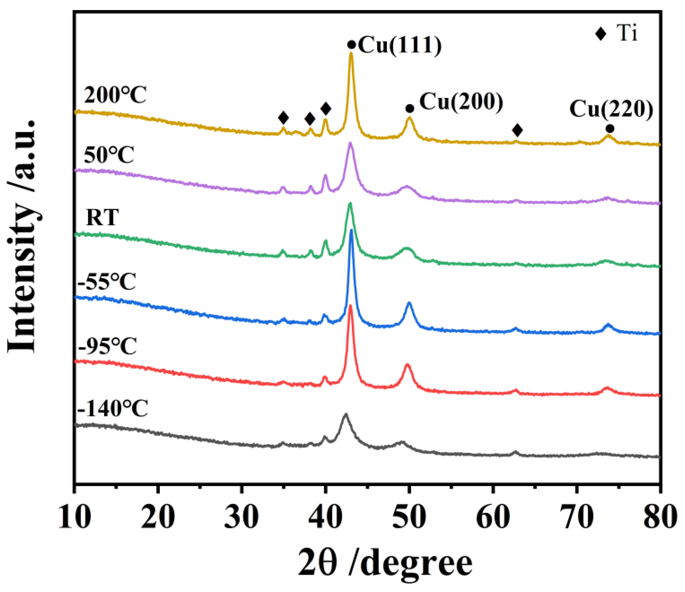
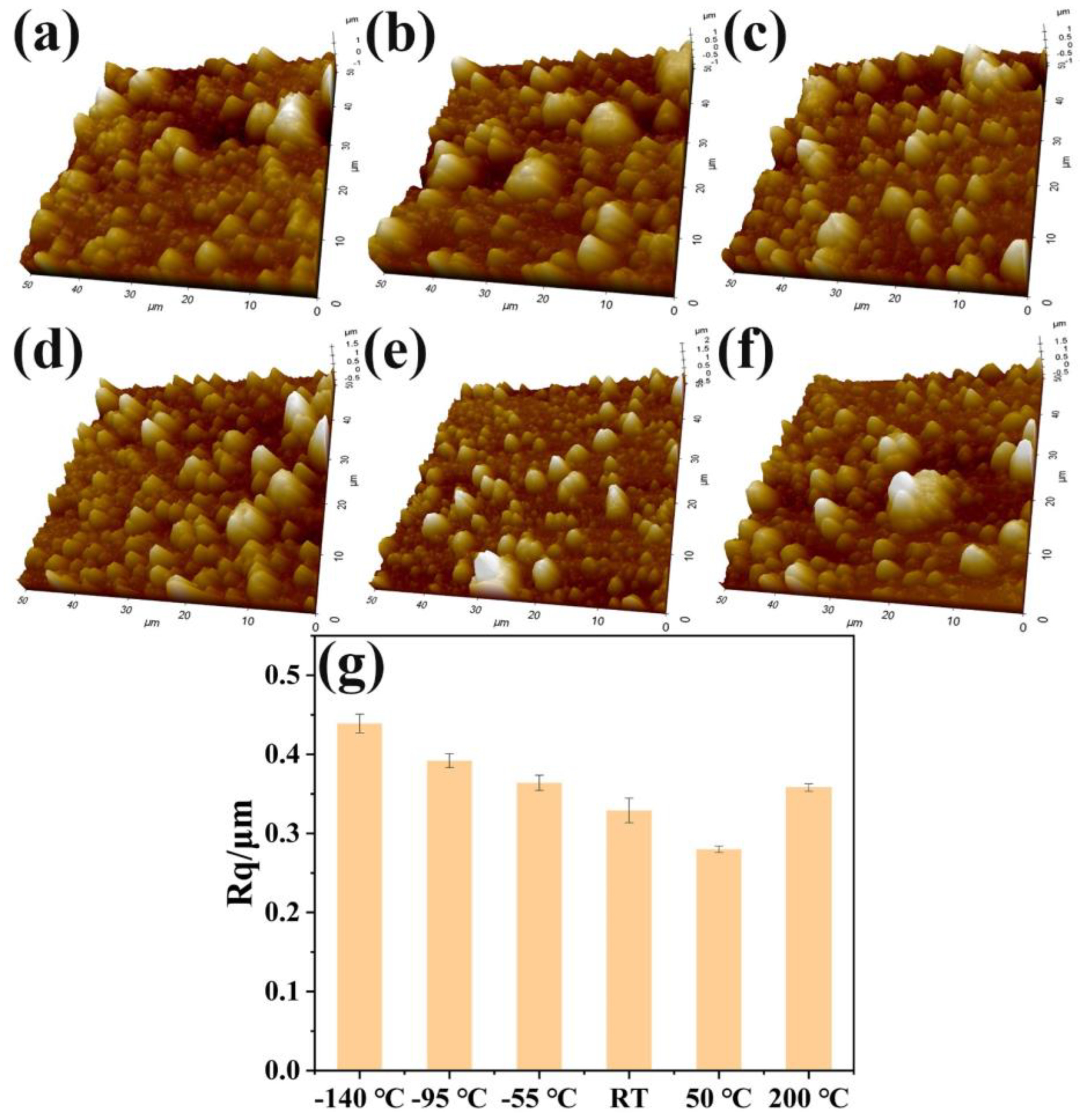
All the Cu films exhibited a strong orientation of the (111) and (200) planes, which is attributed to the lowest surface energy of the (111) plane and lowest strain energy of the (200) plane of the Cu (fcc) crystal. The Cu films deposited at low temperatures below −55 °C exhibited a typical bilayer structure. It can be attributed to the mobility and surface diffusion of the adatoms during the growth of the Cu films. When the deposition temperature increases above the RT, the bilayer structure of Cu films disappears and is replaced by the dense structure.
(2)
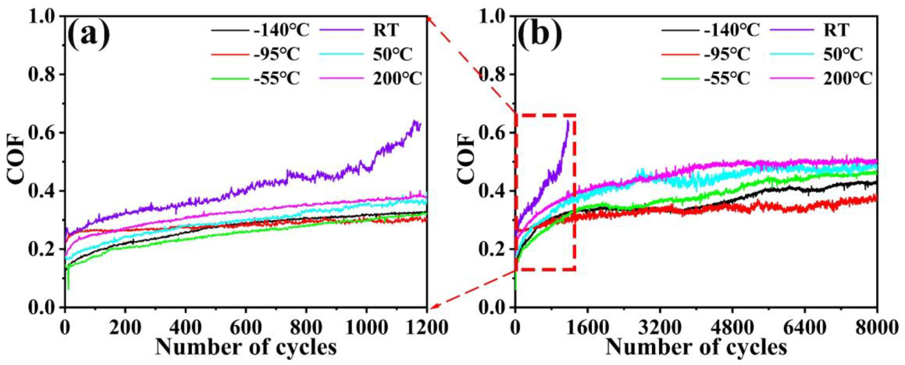
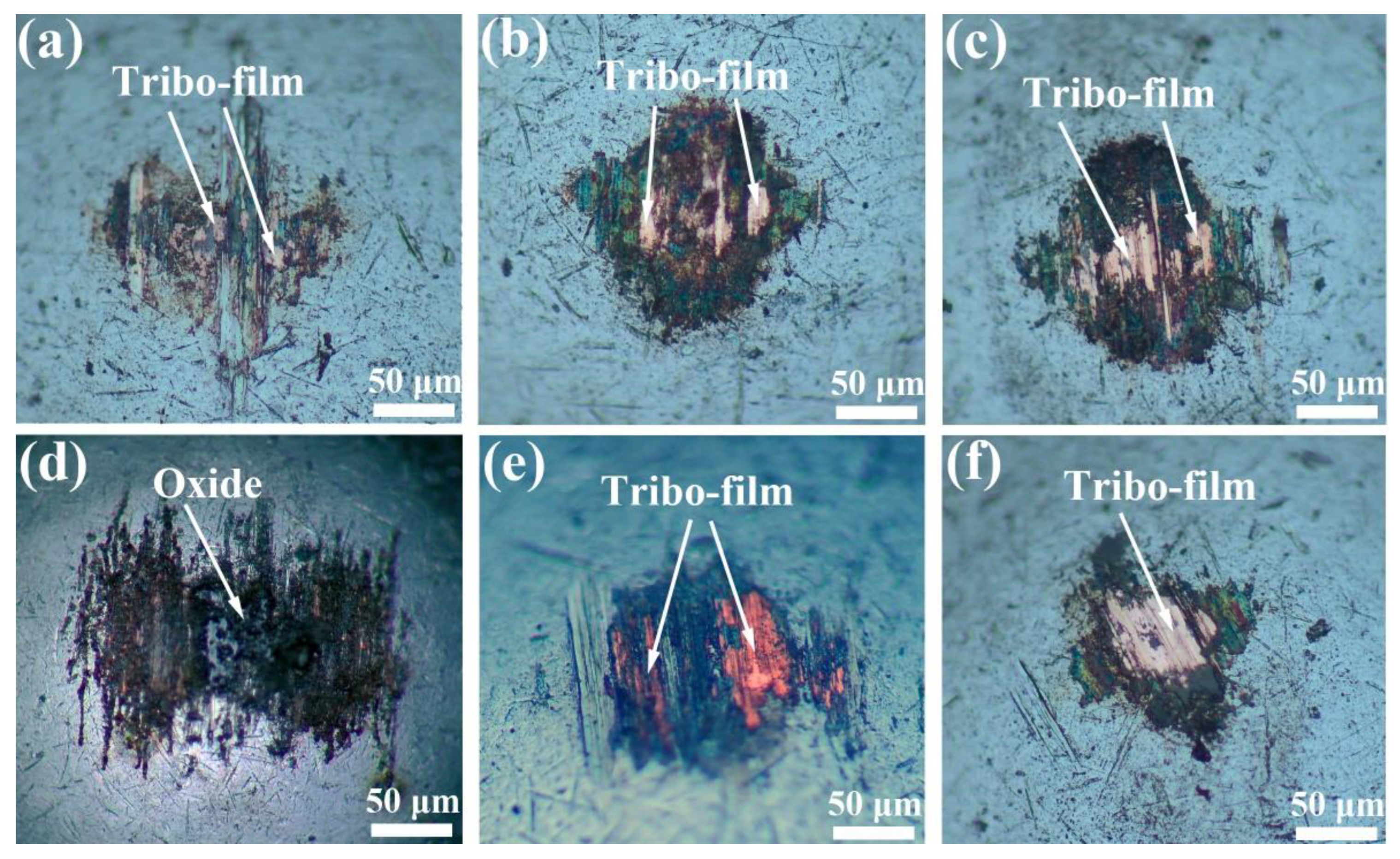
The loose Cu film deposited below −55 °C had relatively stable low friction and anti-wear performances as compared with the Cu film with a dense structure. The loose-structure of Cu film could rearrange on the wear tracks during the current-carrying friction process because the plastic deformation caused by the contact pressure and kinetic frictional interaction easily occurred, which could effectively provide synchronized deformation of the film with the ductile substrate. Furthermore, the transferred softened Cu phase on the tribo-pair surface is conducive to the tribological performance under the current-carrying conditions. Nevertheless, the electric arc can be responsible for the oxidation of Cu phase. This work shows a novel low-temperature deposition strategy of Cu films to improve the friction and wear performances under the electric current condition, and further study would focus on how to enhance its anti-oxidation.

Supplementary Materials

The following supporting information can be downloaded at: https://www.mdpi.com/article/10.3390/lubricants11010008/s1. Figure S1: Optical images of the Wear tracks after 1200 cycles under the current of 0.5 A.

Author Contributions

Conceptualization and methodology: K.L., S.X. and W.L.; software: C.W.; formal analysis and investigation: K.L., S.X. and W.L.; validation: H.Z.; writing—original draft preparation: H.Z.; writing—review and editing: K.L., S.X. and J.S. All authors have read and agreed to the published version of the manuscript.

Funding

The financial support provided by National Natural Science Foundation of China (Grants No. 52075521, U2030201 and 51875563), the fund of State Key Laboratory of Solidification Processing in NWPU (Grant No. SKLSP202002), the fund of LICP Cooperation Foundation for Young Scholars (Grant No. HZJJ22-03), and the fund of Yantai Zhongke Research Institute of Advanced Materials and Green Chemical Engineering (Grant No. AMGCE010).

Data Availability Statement

Not applicable.

Conflicts of Interest

The authors declare no conflict of interest.

Nomenclature

ECRElectrical contact resistance
RaSurface roughness
vThe surface diffusion rate
v0The frequency of atom vibration
DThe average grain diameter
D0The initial grain diameter
nThe grain growth exponent
K(T)The grain growth constant
hThe Plank constant
ΔEThe activation energy
KBThe Boltzmann constant
TTemperature
tTime

References

  1. Holmberg, K.; Erdemir, A. The impact of tribology on energy use and CO2 emission globally and in combustion engine and electric cars. Tribol. Int. 2019, 135, 389–396. [Google Scholar] [CrossRef]
  2. Gong, H.J.; Yu, C.C.; Zhang, L.; Xie, G.X.; Guo, D.; Luo, J.B. Intelligent lubricating materials: A review. Compos. Part B-Eng. 2020, 202, 108450. [Google Scholar] [CrossRef]
  3. Yang, M.S.; Liu, X.B.; Fan, J.W.; He, X.M.; Shi, S.H.; Fu, G.Y.; Wang, M.D.; Chen, S.F. Microstructure and wear behaviors of laser clad NiCr/Cr3C2-WS2 high temperature self-lubricating wear-resistant composite coating. Appl. Surf. Sci. 2012, 258, 3757–3762. [Google Scholar] [CrossRef]
  4. Lu, X.L.; Liu, X.B.; Yu, P.C.; Fu, G.Y.; Zhu, G.X.; Wang, Y.G.; Chen, Y. Effects of annealing on laser clad Ti2SC/CrS self-lubricating anti-wear composite coatings on Ti6Al4V alloy: Microstructure and tribology. Tribol. Int. 2016, 101, 356–363. [Google Scholar] [CrossRef]
  5. Das, A.K. Effect of solid lubricant addition in coating produced by laser cladding process: A review. Mater. Today. Proc. 2022, 56, 1274–1280. [Google Scholar] [CrossRef]
  6. Holmberg, K.; Matthews, A.; Ronkainen, H. Coatings tribology—Contact mechanisms and surface design. New Dir. Tribol. 1998, 251, 107–120. [Google Scholar] [CrossRef]
  7. Holmberg, K.; Ronkainen, H.; Matthews, A. Tribology of thin coatings. Ceram. Int. 2000, 26, 787–795. [Google Scholar] [CrossRef]
  8. Scharf, T.W.; Prasad, S.V. Solid lubricants: A review. J. Mater. Sci. 2013, 48, 511–531. [Google Scholar] [CrossRef]
  9. Aouadi, S.M.; Gao, H.; Martini, A.; Scharf, T.W.; Muratore, C. Lubricious oxide coatings for extreme temperature applications: A review. Surf. Coat. Technol. 2014, 257, 266–277. [Google Scholar] [CrossRef]
  10. Kumar, R.; Hussainova, I.; Rahmani, R.; Antonov, M. Solid Lubrication at High-Temperatures-A Review. Materials 2022, 15, 1695. [Google Scholar] [CrossRef]
  11. Ghotbi, M.Y.; Rahmati, Z. Nanostructured copper and copper oxide thin films fabricated by hydrothermal treatment of copper hydroxide nitrate. Mater. Des. 2015, 85, 719–723. [Google Scholar] [CrossRef]
  12. Kim, K.J.; Kim, J.H.; Kang, J.H. Structural and optical characterization of Cu3N films prepared by reactive RF magnetron sputtering. J. Cryst. Growth 2001, 222, 767–772. [Google Scholar] [CrossRef]
  13. Cale, T.S.; Merchant, T.P.; Borucki, L.J.; Labun, A.H. Topography simulation for the virtual wafer fab. Thin Solid Films 2000, 365, 152–175. [Google Scholar] [CrossRef]
  14. Vancea, J.; Hofmann, F.; Hoffmann, H. Grain size-dependent Hall coefficient in polycrystalline copper films. J. Phys.-Condens. Matter 1989, 1, 7419–7424. [Google Scholar] [CrossRef]
  15. Geetha, M.; Kumar, N.; Panda, K.; Dhara, S.; Dash, S.; Panigrahi, B.K.; Tyagi, A.K.; Jayavel, R.; Kamaraj, V. Tribological and electrical properties of nanocrystalline Cu films deposited by DC magnetron sputtering with varying temperature. Tribol. Int. 2013, 58, 79–84. [Google Scholar] [CrossRef]
  16. Weng, L.; Sun, J.; Ming, H.; Gao, X.; Xue, Q. Structure and tribological properties of Ag films deposited at low temperature. Vacuum 2007, 81, 997–1002. [Google Scholar] [CrossRef]
  17. The, W.; Koh, L.; Chen, S.; Xie, J.; Lie, C.; Fou, P. Study of microstructureand resistivity evolution for electroplated copper films at near room-temperature. Microelectron. J. 2001, 32, 579–585. [Google Scholar] [CrossRef]
  18. Li, X.; Ji, G.; Lv, H.; Min, W.; Du, Y. Microwave absorbing properties and enhanced infrared reflectance of Fe/Cu composites prepared by chemical plating. J. Magn. Magn. Mater. 2014, 355, 65–69. [Google Scholar] [CrossRef]
  19. Bai, P.; Yang, G.R.; You, L.; Lu, T.M.; Knorr, D.B. Room-temperature epitaxy of Cu on Si(111) using partially ionized beam deposition. J. Mater. Res. 1990, 5, 989–997. [Google Scholar] [CrossRef]
  20. Tillmann, W.; Dias, N.; Stangier, D.; Matveev, S.; Debus, J. Design of Cu- and Ag-containing amorphous carbon multilayers with improved tribo-mechanical properties. Mater. Lett. 2020, 284, 128905. [Google Scholar] [CrossRef]
  21. Kataria, S.; Srivastava, S.K.; Kumar, P.; Srinivas, G.; Siju; Khan, J.; Rao, D.; Barshilia, H.C. Nanocrystalline TiN coatings with improved toughness deposited by pulsing the nitrogen flow rate. Surf. Coat. Tech. 2012, 206, 4279–4286. [Google Scholar] [CrossRef]
  22. Cao, Y.; Xia, Y.; Duan, B. Microstructure evolution and anti-wear mechanism of Cu film fabricated by magnetron sputtering deposition. Mater. Lett. 2022, 315, 131941. [Google Scholar] [CrossRef]
  23. Medjani, F.; Sanjines, R.; Allidi, G.; Karimi, A. Effect of substrate temperature and bias voltage on the crystallite orientation in RF magnetron sputtered AIN thin films. Thin Solid Films 2006, 515, 260–265. [Google Scholar] [CrossRef]
  24. Kusaka, K.; Taniguchi, D.; Hanabusa, T.; Tominaga, K. Effect of sputtering gas pressure and nitrogen concentration on crystal orientation and residual stress in sputtered AlN films. Vacuum 2002, 66, 441–446. [Google Scholar] [CrossRef]
  25. Higo, M.; Fujita, K.; Tanaka, Y.; Mitsushio, M.; Yoshidome, T. Surface morphology of metal films deposited on mica at various temperatures observed by atomic force microscopy. Appl. Surf. Sci. 2006, 252, 5083–5099. [Google Scholar] [CrossRef]
  26. Boakye, F. Temperature dependence of the resistivity of amorphous Mn thin films. J. Non-Cryst. Solids 1999, 249, 189–193. [Google Scholar] [CrossRef]
  27. Kale, A.; Seal, S.; Sobczak, N.; Morgiel, J.; Sundaram, K.B. Effect of deposition temperature on the morphology, structure, surface chemistry and mechanical properties of magnetron sputtered Ti70–Al30 thin films on steel substrate. Surf. Coat. Tech. 2001, 141, 252–261. [Google Scholar] [CrossRef]
  28. Seiko, W.; Hoshi, Y.; Shimizu, H. Fe and Fe–N films sputter deposited at liquid nitrogen temperature. J. Magn. Magn. Mater. 2001, 235, 196–200. [Google Scholar] [CrossRef]
  29. Cv, T.; Carel, R. Stress and grain growth in thin films. J. Mech. Phys. Solids 1996, 44, 657–673. [Google Scholar] [CrossRef]
  30. Kumar, A.; Singh, D.; Kumar, R.; Kaur, D. Effect of crystallographic orientation of nanocrystalline TiN on structural, electrical and mechanical properties of TiN/NiTi thin films. J. Alloy. Compd. 2009, 479, 166. [Google Scholar] [CrossRef]
  31. Ma, F.; Zhang, J.M.; Xu, K.W. Surface-energy-driven abnormal grain growth in Cu and Ag films. Appl. Surf. Sci. 2005, 242, 55–61. [Google Scholar] [CrossRef]
  32. Zhang, P.; Zheng, X.; Wu, S.; Liu, J.; He, D. Kinetic Monte Carlo simulation of Cu thin film growth. Vacuum 2004, 72, 405–410. [Google Scholar] [CrossRef]
  33. Su, D.; Yu, M.; Zhang, G.; Jiang, S.; Li, M.Y. High thermal stable Au-Al bimetallic conductive thin films with a broadband transmittance between the UV and NIR regions. J. Mater. Chem. C 2020, 8, 2852–2860. [Google Scholar] [CrossRef]
  34. Su, D.; Jiang, S.L.; Yu, M.N.; Zhang, G.Z.; Liu, H.; Li, M.Y. Facile fabrication of configuration controllable self-assembled Al nanostructures as UV SERS substrates. Nanoscale 2018, 10, 22737–22744. [Google Scholar] [CrossRef] [PubMed]
  35. Morales, C.; Leinen, D.; del Campo, A.; Ares, J.R.; Sanchez, C.; Flege, J.I.; Gutierrez, A.; Prieto, P.; Soriano, L. Growth and characterization of ZnO thin films at low temperatures: From room temperature to-120 degrees C. J. Alloys Compd. 2021, 884, 161056. [Google Scholar] [CrossRef]
  36. Sivakumar, R.; Jayachandran, M.; Sanjeeviraja, C. Studies on the effect of substrate temperature on (VI-VI) textured tungsten oxide (WO3) thin films on glass, SnO2: F substrates by PVD: EBE technique for electrochromic devices. Mater. Chem. Phys. 2004, 87, 439–445. [Google Scholar] [CrossRef]
  37. Zhang, D.M.; Guan, L.; Li, Z.H.; Pan, G.J.; Sun, H.Z.; Tan, X.Y.; Li, L. Influence of kinetic energy and substrate temperature on thin film growth in pulsed laser deposition. Surf. Coat. Technol. 2006, 200, 4027–4031. [Google Scholar] [CrossRef]
  38. Zhao, J.L.; Li, X.M.; Bian, J.M.; Yu, W.D.; Zhang, C.Y. Growth of nitrogen-doped p-type ZnO films by spray pyrolysis and their electrical and optical properties. J. Cryst. Growth 2005, 280, 495–501. [Google Scholar] [CrossRef]
  39. Li, M.Y.; Zhang, Q.Z.; Pandey, P.; Sui, M.; Kim, E.S.; Lee, J. From the Au nano-clusters to the nanoparticles on 4H-SiC (0001). Sci. Rep. 2015, 5, 13954. [Google Scholar] [CrossRef] [Green Version]
  40. Liu, S.; Li, M.-Y.; Su, D.; Yu, M.; Kan, H.; Liu, H.; Wang, X.; Jiang, S. Broadband High Sensitivity ZnO Colloidal Quantum Dots/Self-assembled Au Nano-antennas Heterostructures Photodetectors. ACS Appl. Mater. Interfaces 2018, 10, 32516–32525. [Google Scholar] [CrossRef]
  41. Park, J.Y.; Dong, J.L.; Yun, Y.S.; Moon, J.H.; Lee, B.T.; Sang, S.K. Temperature-induced morphological changes of ZnO grown by metalorganic chemical vapor deposition. J. Cryst. Growth 2005, 276, 158–164. [Google Scholar] [CrossRef]
  42. Park, J.Y.; Lee, J.M.; Je, J.H.; Kim, S.S. Early stage growth behavior of ZnO nanoneedle arrays on Al2O3 (0001) by metalorganic chemical vapor deposition. J. Cryst. Growth 2005, 281, 446–451. [Google Scholar] [CrossRef]
  43. Shin, S.W.; Agawane, G.L.; Kim, I.Y.; Kwon, Y.B.; Jung, I.O.; Gang, M.G.; Moholkar, A.V.; Moon, J.H.; Kim, J.H.; Lee, J.Y. Low temperature epitaxial growth and characterization of Ga-doped ZnO thin films on Al2O3 (0001) substrates prepared with different buffer layers. Appl. Surf. Sci. 2012, 258, 5073–5079. [Google Scholar] [CrossRef]
  44. Petrov, I.; Barna, P.B.; Hultman, L.; Greene, J.E. Microstructural evolution during film growth. J. Vac. Sci. Technol. A 2003, 21, S117–S128. [Google Scholar] [CrossRef]
  45. Chan, K.Y.; Tou, T.Y.; Teo, B.S. Effects of substrate temperature on electrical and structural properties of copper thin films. Microelectron. J. 2006, 37, 930–937. [Google Scholar] [CrossRef]
  46. Xue, J.; Li, Y.; Hao, L.; Gao, L.; Chen, J. Investigation on the interfacial stability of multilayered Cu–W films at elevated deposition temperatures during co-sputtering. Vacuum 2019, 166, 162–169. [Google Scholar] [CrossRef]
  47. Zugelj, B.B.; Kalin, M. Submicron-scale experimental analyses of the multi-asperity contact behaviour of various steels, an aluminium alloy and a polymer. Tribol. Int. 2019, 141, 105955. [Google Scholar] [CrossRef]
  48. Jacobs, T.D.B.; Martini, A. Measuring and Understanding Contact Area at the Nanoscale: A Review. Appl. Mech. Rev. 2017, 69, 060802. [Google Scholar] [CrossRef] [Green Version]
  49. Pan, W.; Li, X.; Wang, X. Contact mechanics of elastic-plastic fractal surfaces and static friction analysis of asperity scale. Eng.Comput. 2020, 38, 131–150. [Google Scholar] [CrossRef]
  50. Chen, J.; Xia, Y.; Hu, Y.; Hou, B. Tribological performance and conductive capacity of Ag coating under boundary lubrication. Tribol. Int. 2017, 110, 161–172. [Google Scholar] [CrossRef]
  51. Lin, X.Z.; Zhu, M.H.; Ji-Liang, M.O.; Chen, G.X.; Jin, X.S.; Zhou, Z.R. Tribological and electric-arc behaviors of carbon/copper pair during sliding friction process with electric current applied. Trans. Nonferrous Met. Soc. China 2011, 21, 292–299. [Google Scholar] [CrossRef]
Figure 1. The system for Cu film deposition with different substrate temperatures.
Lubricants 11 00008 g001
Figure 2. Simple diagram of friction device: 1, metal ball; 2, sample; 3, carrier platform; 4, load-bearing sensor; 5, fixture; 6, reciprocating sliding table; and 7, friction force sensor.
Lubricants 11 00008 g002
Figure 3. XRD spectra of the Cu films deposited at various temperatures.
Lubricants 11 00008 g003
Figure 4. AFM images: (a) −140 °C-Cu, (b) −95 °C-Cu, (c) −55 °C-Cu, (d) RT-Cu, (e) 50 °C-Cu, and (f) 200 °C-Cu, respectively. (g) Surface roughness (Rq) of Cu films versus deposition temperature.
Lubricants 11 00008 g004
Figure 5. SEM surface images: (a) −140 °C-Cu, (b) −95 °C-Cu, (c) −55 °C-Cu, (d) RT-Cu, (e) 50 °C-Cu, and (f) 200 °C-Cu, respectively.
Lubricants 11 00008 g005
Figure 6. SEM cross-sectional images: (a) −140 °C-Cu, (b) −95 °C-Cu, (c) −55 °C -Cu, (d) RT-Cu, (e) 50 °C-Cu, and (f) 200 °C-Cu, respectively.
Lubricants 11 00008 g006
Figure 7. Schematic diagram illustrating fundamental growth processes controlling the microstructural evolution of deposited film.
Lubricants 11 00008 g007
Figure 8. Friction coefficient curves of Cu films on 304 SS substrates: (a) The initial sliding of 1200 cycles; (b) The long sliding of 8000 cycles.
Lubricants 11 00008 g008
Figure 9. 3D images and the cross-section profiles of wear tracks: (a,a1) −140 °C-Cu, (b,b1) −95 °C-Cu, (c,c1) −55 °C-Cu, (d,d1) 50 °C-Cu, and (e,e1) 200 °C-Cu, respectively.
Lubricants 11 00008 g009
Figure 10. SEM images of the wear track after 8000 cycles: (a) −140 °C-Cu, (b) −95 °C-Cu, (c) −55 °C- Cu, (d) 50 °C-Cu, and (e) 200 °C-Cu, respectively.
Lubricants 11 00008 g010
Figure 11. (a) Evolution of ECR curves of Cu films at the electric current-carrying of 0.5 A; (b) Friction coefficient curves at the electric current-carrying of 0.5 A; and (c) Wear width at the electric current-carrying of 0.5 A.
Lubricants 11 00008 g011
Figure 12. The corresponding (a) schematic diagram of the current circuit during the rubbing process and (b) schematic diagram of the wear mechanism.
Lubricants 11 00008 g012
Figure 13. Three-dimensional images and the cross-section profiles of wear tracks: (a,a1) −140 °C-Cu, (b,b1) −95 °C-Cu, (c,c1) −55°C-Cu, (d,d1) RT-Cu, (e,e1) 50 °C-Cu, and (f,f1) 200 °C-Cu, respectively, under the electric current-carrying of 0.5 A.
Lubricants 11 00008 g013
Figure 14. Friction coefficient curves of the Cu films under the electric current-carrying of 1.0 A.
Lubricants 11 00008 g014
Figure 15. Three-dimensional images and the cross-section profiles of wear tracks: (a,a1) −140 °C-Cu, (b,b1) −95 °C-Cu, (c,c1) −55 °C-Cu, (d,d1) RT-Cu, (e,e1) 50 °C-Cu, and (f,f1) 200 °C-Cu, respectively, under the electric current-carrying of 1.0 A.
Lubricants 11 00008 g015
Figure 16. SEM images of wear track: (a) −95 °C Cu at the electric current-carrying of 0.5 A, (b) RT Cu at the electric current-carrying of 0.5 A, and (c) RT Cu at the electric current-carrying of 1.0 A, respectively.
Lubricants 11 00008 g016
Figure 17. Wear scars on the 304 SS ball sliding against the Cu film: (a) −140 °C Cu, (b) −95 °C Cu, (c) −55 °C Cu, (d) RT Cu, (e) 50 °C Cu, and (f) 200 °C Cu under the electric current-carrying of 1 A.
Lubricants 11 00008 g017
Table 1. Typical deposition conditions for the Ti buffer layer.
Ar pressure0.5 Pa
Substrate bias voltage50 V
Target current80 A
Target voltage20 V
Deposition time20 min
Sputtering temperature200 °C
Table 2. Typical deposition conditions for Cu film.
Standard pressure5 × 10−3 Pa
Working pressure0.3 Pa
Target current0.5 A
Target voltage400 V
Deposition time5 min
Target distance60 mm
Ar flow rate100 sccm
Substrate temperature−140 °C, −95 °C, −55 °C,
RT, 50 °C, 200 °C
Table 3. EDS analysis of region denoted by Mark 1, 2, and 3 in Figure 16 (Wt.%.).
RegionOTiFeCu
Mark 12.2%16.0%1.2%80.6%
Mark 221.8%71.1%07.1%
Mark 342.9%30.4%26.7%0
Disclaimer/Publisher’s Note: The statements, opinions and data contained in all publications are solely those of the individual author(s) and contributor(s) and not of MDPI and/or the editor(s). MDPI and/or the editor(s) disclaim responsibility for any injury to people or property resulting from any ideas, methods, instructions or products referred to in the content.

