Article

Measurement of Film Structure Using Time-Frequency-Domain Fitting and White-Light Scanning Interferometry

State Key Laboratory of Precision Measuring Technology and Instruments, Tianjin University, Tianjin 300072, China
*
Author to whom correspondence should be addressed.
Machines 2021, 9(12), 336; https://doi.org/10.3390/machines9120336
Submission received: 16 October 2021 / Revised: 24 November 2021 / Accepted: 6 December 2021 / Published: 7 December 2021
(This article belongs to the Special Issue Precision Measurement and Machines)

Abstract

:
A new technique is proposed for measuring film structure based on the combination of time- and frequency-domain fitting and white-light scanning interferometry. The approach requires only single scanning and employs a fitting method to obtain the film thickness and the upper surface height in the frequency and time domains, respectively. The cross-correlation function is applied to obtain the initial value of the upper surface height, thereby making the fitting process more accurate. Standard films (SiO2) with different thicknesses were measured to verify the accuracy and reliability of the proposed method, and the three-dimensional topographies of the upper and lower surfaces of the films were reconstructed.

1. Introduction

Fabrication processes in the semiconductor and display industries invariably involve continuous deposition and etching to integrate thin films on silicon substrates or transparent glass, and measuring the film thickness and topography is essential for increasing yields and monitoring product quality. Spectroscopic reflectometers are used widely to measure the thickness and the refractive index of thin films by observing the intensity of reflected light [1,2,3], and ellipsometry is well-known in thin-film measurement for its high precision and accuracy [4,5,6,7]. However, those methods give only the film thickness, whereas it is also necessary to obtain the upper or lower surface height when measuring the topography. The film thickness and height can be estimated from the phase information of a white-light spectral interferometer (WSI) [8,9,10], but WSIs cannot be applied to full-field measurement and have low lateral resolution.
Instead, the surface topography can be obtained using white-light vertical scanning interferometers (VSIs) [11,12,13]. Limited by the coherence length of the light source, traditional VSI analysis methods such as coherent peak detection (CPD) algorithms can only obtain the thicknesses of relatively thick films [14]. For measuring thin films, frequency-domain analysis is usually required. The phase analysis in the frequency domain determines the film thickness through the nonlinear phase caused by the film [15,16]. This method is not reliable when the thickness is less than 100 nm, and the approach relies on the accuracy of the initial value of the fitting and the removal of the nonlinear phase of the measurement system. de Groot and de Lega proposed a VSI signal model [17], and several researchers have used it to obtain the film reflectivity and thickness from Fourier-transform information [18,19,20]. In those methods, the tested sample is compared with a reference sample to solve the film-thickness issue, but such approaches usually require the tested and reference samples to be scanned separately and the light-source intensity and experimental parameters to remain consistent in the two measurements, thereby setting higher requirements for the experimental equipment and operation [21,22,23,24].
Herein, we propose a method for measuring films in the full field of view based on single VSI scanning. The method exploits the phenomenon that the VSI signals of different film thicknesses have different amplitude shapes in the frequency domain; the thickness of the film is measured via frequency-domain amplitude fitting, and the height of the upper surface of the film is measured through the time-domain fitting of the VSI signal. In the proposed method, the tested sample requires only one vertical scan to measure the film thickness and the height of the upper surface, whereupon the three-dimensional (3D) topographies of the upper and lower surfaces of the film are reconstructed.

2. System Setup and Measurement Principle

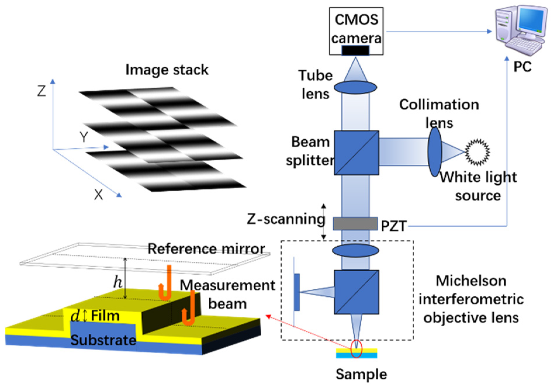
2.1. System Structure

The experimental configuration is presented in Figure 1. A Michelson-type VSI was used as the optical system. A 5× interference objective lens (CF EPI Plan TI 5×; Nikon, Tokyo, Japan) and a 1× tube lens were used to form an image on the camera, where the lateral resolution was 2.1 μm. A coaxial illumination beam from a halogen lamp was used as the light source, and the camera (acA1300-200 um CMOS; Basler, Ahrensburg, Germany) featured 1280 × 1024 pixels with a pixel size of 4.8 μm × 4.8 μm. A piezoelectric transducer (PZT) afforded precise scanning in the Z direction and featured a high-precision objective scanner (P-721; Physik Instrumente, Karsruhe, Germany). The PZT used a capacitive sensor with a stroke of 100 μm in the closed-loop mode and had a resolution of 0.7 nm, a linear error of 0.03 nm, and a repeatability of ±5 nm. The system was placed on an active vibration-isolation table to reduce the influence of external vibrations.

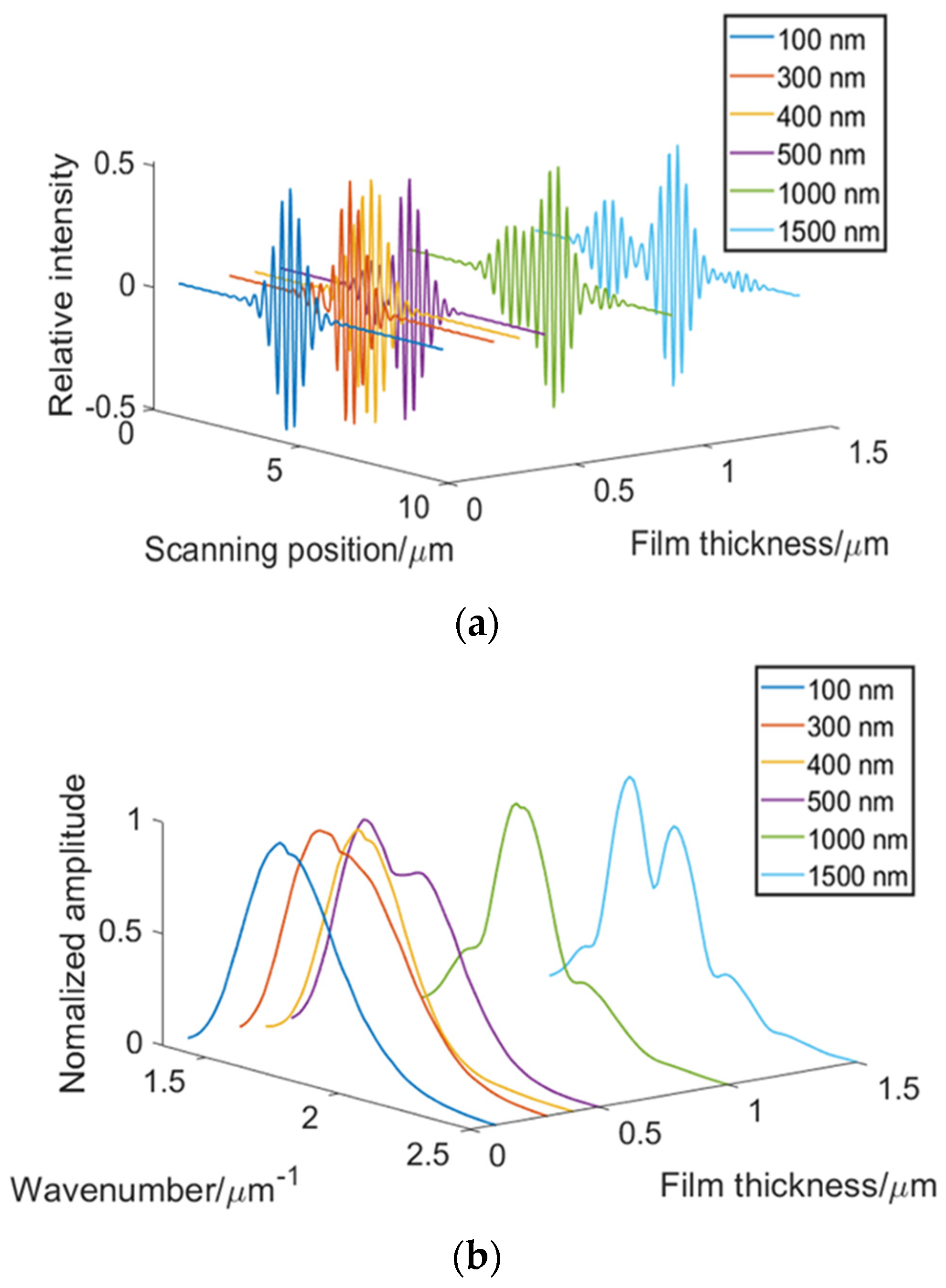
2.2. VSI Modeling for Film Samples

According to the interference theory, the intensity of the interfering light can be expressed as:
I = I r + I s + 2 I r I s   c o s   δ ,
where I r and I s are the light intensities of the reference and sample light beams, respectively, and δ is the phase difference between the two beams.
The light intensity and phase of the reflected light will change, when the sample is a thin film. The Fresnel equations are used to describe this model [25]. The total reflection coefficient R can be expressed as:
R = r 12 + r 23 e x p ( j 2 π d k N 2 c o s   θ ) r 12 + r 12 r 23 e x p ( j 2 π d k N 2 c o s   θ ) ,
where r 12 and r 23 are the Fresnel reflection coefficients of the upper and lower surfaces of the film, respectively, d is the film thickness, N 2 is the complex refractive index of the film, and θ is the incidence angle.
The square of the modulus of the total reflection coefficient R o b j = | R | 2 represents the ratio of the intensity of the reflected light to the intensity of the incident light, and the phase R represents the phase caused by the film. If the ratio of the light intensity passing through the beam splitter is m r : m s and m r + m s = 1 and if the reflectivity of the reference mirror is R r e f , then the influence of the numerical aperture of the objective lens may be ignored. If the intensity of the light reflected by the reference mirror is I r e f ( k ) , then by combining Equations (1) and (2), the VSI signal of a film with wavenumber k = 1 λ can be expressed as:
I ( k , z ) = I r e f ( k ) [ 1 + c ( k ) R o b j + 2 c ( k ) R o b j c o s ( ϕ ) ] ,
where c ( k ) = m s m r R r e f is the calibration coefficient, ϕ = 4 π k ( h z ) + R is the phase difference, z is the scanning position, and h is the height of the upper surface. The position of the reference mirror in Figure 1 is the zero point of the scanning position, and the scanning direction from bottom to top is defined as the positive direction. When measuring films thinner than 100 nm, the parameter c ( k ) must be calibrated to ensure more accurate results; we discuss this in Section 3.2.
When the signal is collected by a digital camera with a spectral response of G ( k ) , the interference signal of white light is the integral of the interference signal between wavenumbers k 1 and k 2 and can be written as:
I ( z ) = k 1 k 2 G ( k ) I ( k , z ) d k .

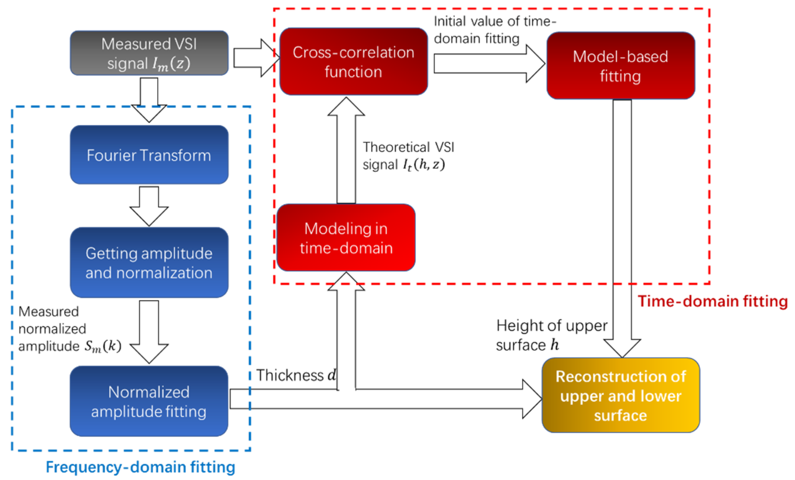
2.3. Time- and Frequency-Domain Fitting

In this section, we will combine the VSI signal model of the film sample to describe a method of film topography reconstruction based on the time- and frequency-domain fitting. The time domain here is the domain of the original VSI signal, and the frequency domain is the domain of the VSI signal after Fourier transform.
In this method, the film thickness d is calculated by frequency-domain fitting, and the height of the upper surface of the film h is obtained by time-domain fitting. The height of the lower surface can be calculated by subtracting the thickness of the film d from the height of the upper surface h . The topography of the film is reconstructed by this process. The flowchart of the proposed method is shown in Figure 2.
The time-and frequency-domain fitting and simulation will be described in detail below.

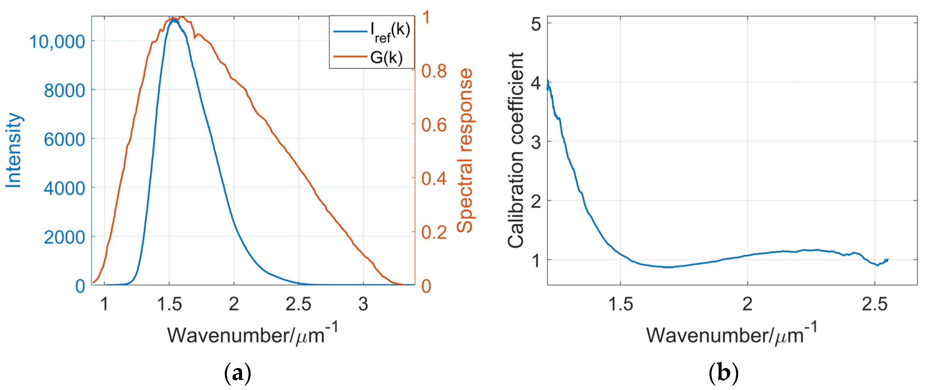
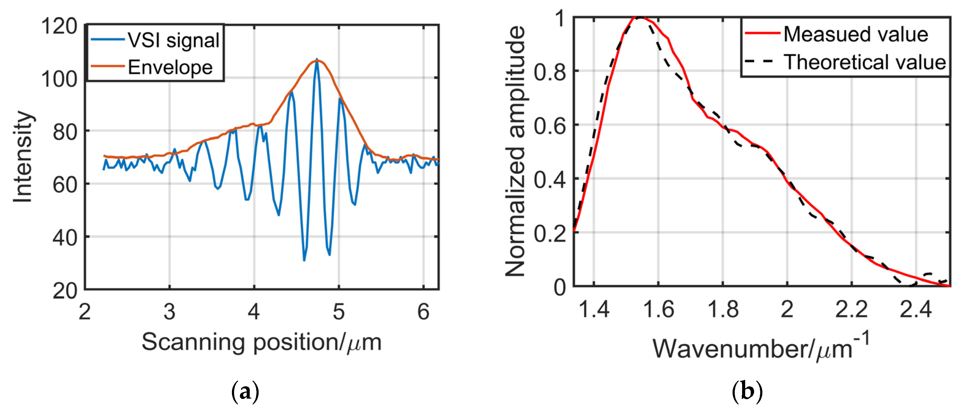
2.3.1. Principle of the Frequency-Domain Fitting

Equations (3) and (4) show that the interference signal for each wavenumber k is a DC signal G ( k ) I r e f ( k ) ( 1 + c   ( k ) R o b j ) plus a cosine signal with an amplitude of 2 G ( k ) I r e f ( k ) c ( k ) R o b j . If the interference signal I ( z ) is Fourier-transformed, then the time-domain signal is transformed into the frequency domain and is shown as:
S ( k ) = + I ( z ) e x p ( j 4 π z k ) d z .
The amplitude of the frequency domain can be regarded as the intensity of the light source modulated by the film. Therefore, the film-thickness information can be obtained through the amplitude information. Normalizing the Fourier-transform amplitude of the visible-light band can make this method insensitive to changes in the overall intensity of the spectrum of the light source, as long as the spectral shape remains constant.
The frequency-domain analysis of the interference signal was illustrated by simulation. In Figure 3a, Equation (4) was used to simulate the VSI signal of a thin SiO2 film deposited on a silicon substrate with different film thicknesses of 100, 300, 400, 500, 1000, and 1500 nm, and the scanning step was 30 nm. The white-light source was set as a Gaussian light source (full width at half maximum, 140 nm; central wavelength, 580 nm). Assuming that the light intensity ratio of the two beams which the white light source is split into by a beam splitter is 1:1, for the visible light, the reflectivity of the reference mirror can be regarded as 1. Figure 3b shows that the normalized amplitudes differed obviously with different film thicknesses.
Therefore, the Fourier-transform-normalized amplitude S m ( k ) of the measurement data can be compared with the theoretical Fourier-transform-normalized amplitude S t ( k , d ) by minimizing the parameter e ( d ) , which can be expressed as:
e ( d ) = k m i n k m a x ( S t ( k , d ) S m ( k ) ) 2 .
Given that this method is a Fourier-transform-based method, for discrete signals, the accuracy of the scanning step has an impact on the measurement results, especially for extremely thin films. The influences of the step error of the scanner on the measurements of films with different thicknesses were simulated. The simulation generated signals of five different thicknesses for SiO2, i.e., 1000, 300, 100, 80, and 50 nm with a scanning step of 30 nm. Table 1 lists the mean values and standard deviations of the film thicknesses for 10 measurements after adding Gaussian noise (zero mean and standard deviations of 1 and 5 nm) to the scanning step. Table 1 shows that when the film thickness was less than 100 nm, the error of the scanning step had a greater impact on the measurement results of the film thickness. Therefore, when measuring extremely thin films, this method requires a highly accurate scanning step.

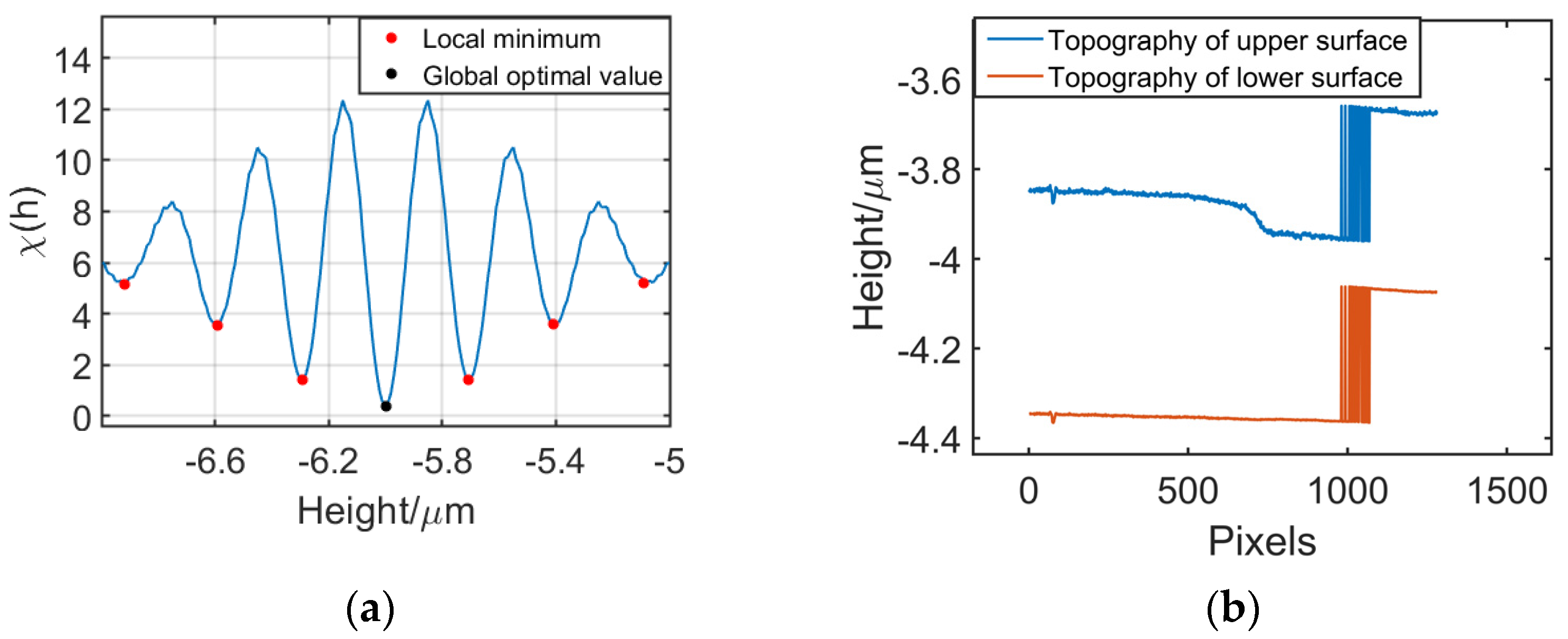
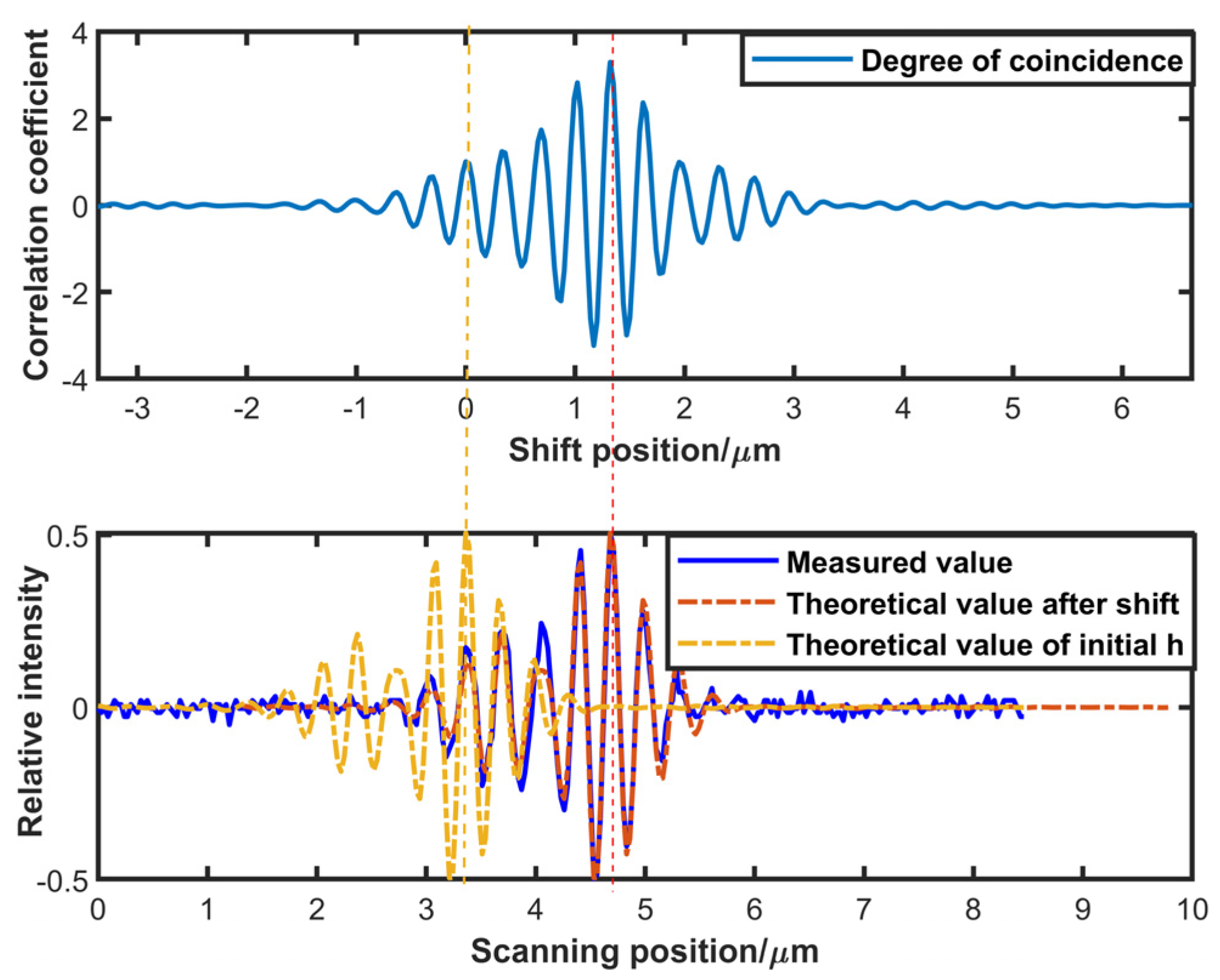
2.3.2. Principle of the Time-Domain Fitting

After determining the film thickness d, the height of the upper surface h is determined to reconstruct the surface topography of the film. Given that the VSI signal in the time domain is also a function of the upper surface height h, the nonlinear fitting of the time-domain signal can also be used to determine the upper surface height of the film, when the residual χ ( h )   is minimum, which can be described as:
χ ( h ) = z s t a r t   z e n d ( I t ( h , z ) I m ( z ) ) 2 ,
where I m ( z ) is the measured time-domain signal, and I t ( h , z ) is the theoretical time-domain signal obtained by bringing the thickness d from the frequency-domain fitting into Equation (4). We simulated the signal with an upper surface height of h = −6 μm and a film thickness of 400 nm. Figure 4a shows the residuals χ ( h ) of the time-domain fitting, and as shown in Figure 4b, there were many local minima that could cause incorrect results if the initial fitting value was not suitable.
Each h in the search range was substituted into the model to calculate the residual of the theoretical and measured values according to Equation (7). However, Equation (3) shows that the time-domain fitting is a process whereby the measured and theoretical values are shifted to the maximum degree of coincidence. Therefore, the cross-correlation function can be applied to determine the height value, which can be written as:
R ( m ) = z s t a r t z e n d I t ( z + m ) I m ( z ) .
As shown in Figure 5, when processing the experimental data, we calculated one theoretical value for the initial value of the height. Then, we shifted it and calculated the degree of coincidence (cross-correlation coefficient R ( m ) ) between the theoretical and measured values through the cross-correlation function. When the cross-correlation coefficient was maximized, the offset was added to the original initial value of the height to obtain the value of the height. Compared with Equation (7), only one theoretical value needed to be calculated, thereby accelerating the calculation. However, the accuracy of the height value obtained was limited by the scanning step. Equation (8) can be used to quickly determine an initial height value near the global optimal value, and a more accurate height value can be obtained by Equation (7).
Noises with signal-to-noise ratios (SNRs) of 35, 30, and 25 dB were added to the simulation signal (the height was −6 μm, and the thickness was 300 nm), and the results for 10 simulation measurements are given in Table 2. The SNR during the experiment was typically 30–40 dB. Table 2 shows that this method is insensitive to noise when measuring the height.
After obtaining the film thickness and the upper surface height, the height of lower surface can be calculated by subtracting the thickness of the film d from the height of the upper surface h . The upper and lower surfaces of the film can be reconstructed.

3. Experiments and Discussion

3.1. System Structure

Before measurement, the system parameters in Equations (3) and (4) must be calibrated. First, the spectrum of the light reflected from the reference mirror (corresponding to I r e f ( k ) in Equation (3)) was measured by a spectrometer (QE Pro; Ocean Optics, Dunedin, USA) when the measuring optical path is blocked, and the spectral response of the camera (corresponding to G ( k ) in Equation (4)) was obtained from the camera’s manual; these are shown in Figure 6a.
Second, the calibration coefficient c ( k ) was obtained by Equation (9) using a bare silicon sample, where I s i l i c o n is the reflection spectrum of the silicon at the measuring path when the reference optical path is blocked, and R s i l i c o n is the reflectivity of silicon, shown as following:
c ( k ) = I s i l i c o n I r e f R s i l i c o n .

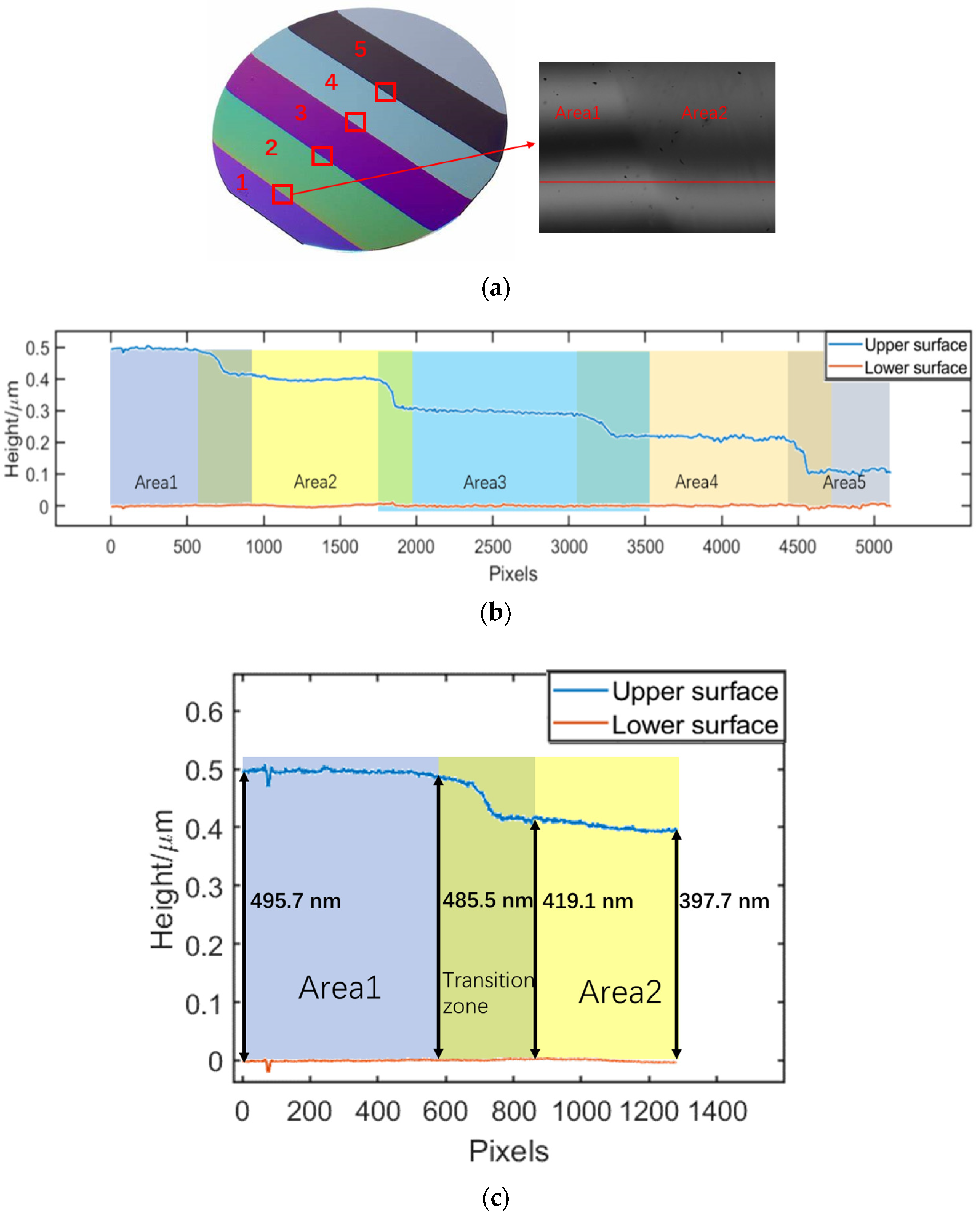
3.2. Thickness Measurement

A stepped film of SiO2 deposited on a Si substrate (from Ocean Optics) was measured to verify the frequency-domain fitting method, and there were five regions with different thicknesses numbered 1–5 on the sample (Figure 7a). Table 3 lists the calibrated thickness values, the measured average thickness values, and the standard deviations obtained by repeated measurements at pixel (640, 512) of regions 1–5 using the proposed method. The errors between the mean values of the measurement and the calibration values were below 1.9%, and the relative standard deviations were below 1.7%. Thus, the accuracy and reliability of the proposed method for measuring film thickness have been demonstrated.
Taking the measurement process at area 3 (where the calibrated film thickness was 298.65 nm) as an example, Figure 7a shows the VSI signal collected in this area. It is difficult to separate the peaks for the upper and lower surfaces using the CPD algorithms in the time domain. We collected 283 points in the time domain, and the frequency-domain resolution was improved through zero padding. In Figure 7b, the solid red line is the Fourier-transform-normalized amplitude of the VSI signal obtained from the experiment, and the wavenumber range was 1.33–2.5 µm−1 (400–750 nm). The black dashed line is the theoretical Fourier-transform-normalized amplitude, and the coefficient of correlation between the measured and theoretical values was 0.9970.
We also measured the thicknesses values of thicker films (from UniversityWafer, Inc., Boston, MI, USA). Table 4 lists the results of repeated measurements at pixel (640, 512) obtained by the normalized amplitude fitting and the CPD algorithm. Because only the refractive index at the center wavelength of the light source was used in the CPD algorithm whereas normalized amplitude fitting used the information of the entire waveband, the thickness value obtained by the proposed method was more accurate.
When the film thickness was less than 100 nm, the characteristic of the signal was very weak, and the measurement was sensitive to the calibration coefficient c ( k ) in the signal model. Table 5 lists the measurement results of five measurements at pixel (640, 512) for thinner films (from Filmetrics, Inc., San Diego, CA, USA) with and without calibration. A 5 × 5-pixel averaging filter was applied to each image to reduce the impact of noise as much as possible. In future work, the results will be improved by isolating environmental disturbances and using a more accurate scanning step during measurement.

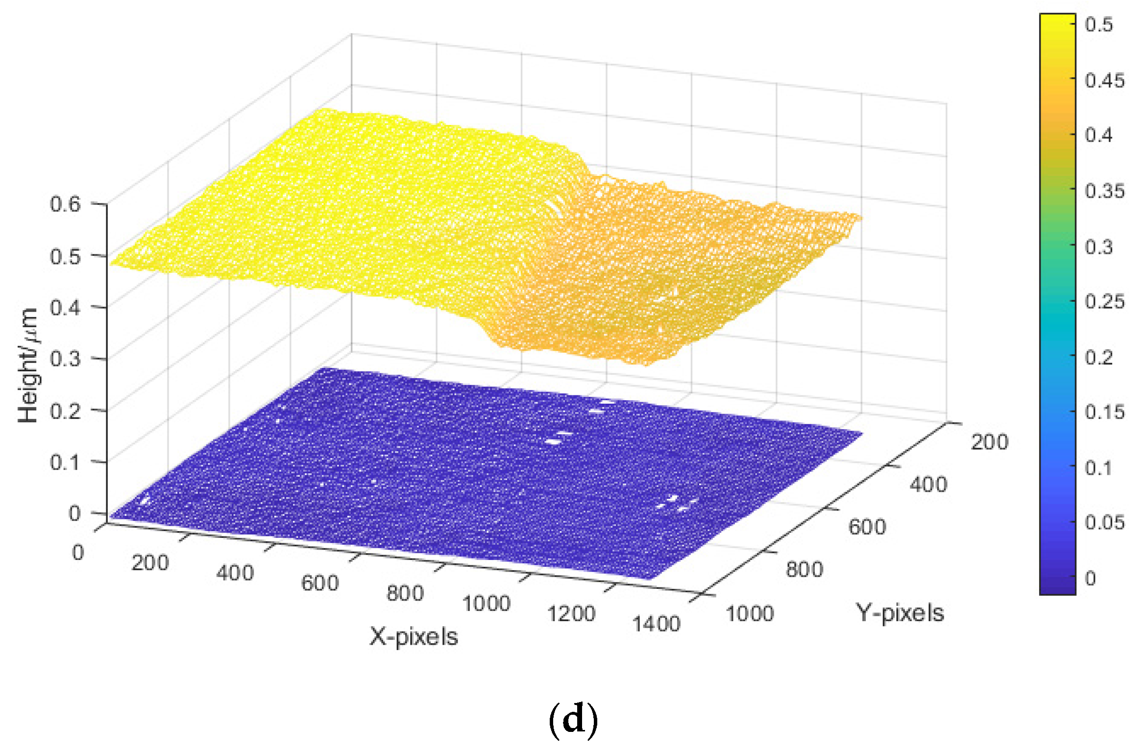
3.3. Surface Topography Reconstruction

For the stepped film, at the junctions between areas of different thicknesses, the film was not as uniform as in other areas. There was a stepped height area on the upper surface, and the lower surface was a silicon plane. Thus, we proceeded to reconstruct the upper and lower surfaces of the region of interest by the time-domain fitting method. The cross-sectional morphologies of the junctions of different thicknesses shown in the red squares in Figure 8a were spliced together in Figure 8b, and more details of the junction between areas 1 and 2 (the red line in Figure 8a) are shown in Figure 8c. Because of the high lateral resolution of the full-field-of-view measurement, we can observe the transition of the surface topography at the junction. The range of the film thickness was approximately 400–500 nm, and the maximum and minimum thicknesses of the transition zone were 485.8 and 419.1 nm, respectively. As shown in Figure 8d, pixels in lines 310–1000 were selected for 3D surface topography reconstruction. The lower surface of the reconstructed film was almost a plane, which proved the accuracy of the height obtained by the time-domain fitting.

4. Conclusions

In this study, we have proposed a film measurement method based on time- and frequency-domain fitting of a VSI model. We exploited the fact that the signal shape of the Fourier-transform-normalized amplitude in the frequency domain is determined only by the film thickness. Thus, the film thickness was obtained through nonlinear fitting, and the fitting of the time-domain signal was used to reconstruct the upper surface of the film. Standard SiO2 films of different thicknesses were measured to verify the accuracy and reliability of this measurement method, and the surface topographies of the junctions between film steps with different thicknesses were measured, thereby enabling the 3D topographies of the upper and lower surfaces to be reconstructed.

Author Contributions

Conceptualization, X.G. and T.G.; methodology, X.G.; software, X.G. and L.Y.; validation, X.G. and T.G.; formal analysis, X.G.; investigation, X.G. and T.G.; resources, T.G. and L.Y.; data curation, X.G.; writing—original draft preparation, X.G.; writing—review and editing, T.G., X.G. and L.Y.; visualization, X.G.; supervision, T.G.; project administration, T.G.; funding acquisition, T.G. All authors have read and agreed to the published version of the manuscript.

Funding

This research was funded by National Key Research and Development Program of China (grant No. 2017YFF0107001) and the 111 Project fund (grant No. B07014).

Institutional Review Board Statement

Not applicable.

Informed Consent Statement

Not applicable.

Data Availability Statement

Data are contained within the article.

Conflicts of Interest

The authors declare no conflict of interest.

References

  1. Kim, M.G.; Kim, J.Y. Measurement of two-dimensional thickness of micro-patterned thin film based on image restoration in a spectroscopic imaging reflectometer. Appl. Opt. 2018, 57, 3423–3428. [Google Scholar] [CrossRef] [PubMed]
  2. Kim, M.G. Improvement of spectral resolution in spectroscopic imaging reflectometer using rotating-type filter and tunable aperture. Meas. Sci. Technol. 2018, 10, 105001. [Google Scholar] [CrossRef]
  3. Choi, G.; Lee, Y.; Lee, S.W.; Cho, Y.; Pahk, H.J. Simple method for volumetric thickness measurement using a color camera. Appl. Opt. 2018, 57, 7550–7558. [Google Scholar] [CrossRef]
  4. Kajihara, Y.; Fukuzawa, K.; Itoh, S.; Watanabe, R.; Zhang, H. Theoretical and experimental study on two-stage-imaging microscopy using ellipsometric contrast for real-time visualization of molecularly thin films. Rev. Sci. Instrum. 2013, 84, 053704. [Google Scholar] [CrossRef] [PubMed]
  5. Aspnes, D.E. Studies of surface, thin film and interface properties by automatic spectroscopic ellipsometry. J. Vac. Sci. Technol. 1981, 18, 289–295. [Google Scholar] [CrossRef]
  6. Lee, S.W.; Choi, G.; Lee, S.Y.; Cho, Y.; Pahk, H.J. Coaxial spectroscopic imaging ellipsometry for volumetric thickness measurement. Appl. Opt. 2021, 60, 67–74. [Google Scholar] [CrossRef] [PubMed]
  7. Ohlídal, I.; Vohánka, J.; Buršíková, V.; Franta, D.; Čermák, M. Spectroscopic ellipsometry of inhomogeneous thin films exhibiting thickness non-uniformity and transition layers. Opt. Express 2020, 28, 160–174. [Google Scholar] [CrossRef] [PubMed]
  8. Ghim, Y.S.; Rhee, H.G.; Yang, H.S.; Lee, Y.W. Thin-film thickness profile measurement using a Mirau-type low-coherence interferometer. Meas. Sci. Technol. 2013, 24, 075002. [Google Scholar] [CrossRef]
  9. Guo, T.; Chen, Z.; Li, M.; Wu, J.; Fu, X.; Hu, X. Film thickness measurement based on nonlinear phase analysis using a Linnik microscopic white-light spectral interferometer. Appl. Opt. 2018, 57, 2955–2961. [Google Scholar] [CrossRef] [PubMed]
  10. Guo, T.; Zhao, G.; Tang, D.; Weng, Q.; Sun, C.; Gao, F.; Jiang, X. High-accuracy simultaneous measurement of surface profile and film thickness using line-field white-light dispersive interferometer. Opt. Laser Eng. 2021, 137, 106388. [Google Scholar] [CrossRef]
  11. Lee, B.S.; Strand, T.C. Profilometry with a coherence scanning microscope. Appl. Opt. 1990, 29, 3784–3788. [Google Scholar] [CrossRef] [PubMed]
  12. Dresel, T.; Häusler, G.; Venzke, H. Three-dimensional sensing of rough surfaces by coherence radar. Appl. Opt. 1992, 31, 919–925. [Google Scholar] [CrossRef]
  13. De Groot, P.; Deck, L. Three-dimensional imaging by sub-Nyquist sampling of white-light interferograms. Opt. Lett. 1993, 18, 1462–1464. [Google Scholar] [CrossRef] [Green Version]
  14. Ma, L.; Guo, T.; Yuan, F.; Zhao, J.; Fu, X.; Hu, X. Thick film geometric parameters measurement by white light interferometry. In Proceedings of the SPIE Asia Communications and Photonics, Shanghai, China, 19 October 2009. [Google Scholar] [CrossRef]
  15. Kim, S.W.; Kim, G.H. Thickness-profile measurement of transparent thin-film layers by white-light scanning interferometry. Appl. Opt. 1999, 38, 5968–5973. [Google Scholar] [CrossRef] [PubMed]
  16. Chen, K.; Lei, F.; Itoh, M. Efficient phase matching algorithm for measurements of ultrathin indium tin oxide film thickness in white light interferometry. Opt. Rev. 2017, 24, 121–127. [Google Scholar] [CrossRef]
  17. De Groot, P.; de Lega, X.C. Signal modeling for low-coherence height-scanning interference microscopy. Appl. Opt. 2004, 43, 4821–4830. [Google Scholar] [CrossRef] [PubMed]
  18. Kim, J.Y.; Kim, S.; Kim, M.G.; Pahk, H.J. Generating a True Color Image with Data from Scanning White-Light Interferometry by Using a Fourier Transform. Curr. Opt. Photon. 2019, 3, 408–414. [Google Scholar]
  19. Daniel, M. The distorted helix: Thin film extraction from scanning white light interferometry. In Proceedings of the SPIE Integrated Optics, Silicon Photonics, and Photonic Integrated Circuits, Strasbourg, France, 3–7 April 2006. [Google Scholar] [CrossRef]
  20. Maniscalco, B.; Kaminski, P.M.; Walls, J.M. Thin film thickness measurements using Scanning White Light Interferometry. Thin Solid Films 2014, 550, 10–16. [Google Scholar] [CrossRef] [Green Version]
  21. Claveau, R.; Montgomery, P.; Flury, M. Coherence scanning interferometry allows accurate characterization of micrometric spherical particles contained in complex media. Ultramicroscopy 2020, 208, 112859. [Google Scholar] [CrossRef] [PubMed]
  22. Claveau, R.; Montgomery, P.C.; Flury, M.; Montaner, D. Local reflectance spectra measurements of surfaces using coherence scanning interferometry. In Proceedings of the SPIE Photonics Europe, Brussels, Belgium, 4–7 April 2016. [Google Scholar] [CrossRef]
  23. Marbach, S.; Claveau, R.; Wang, F.; Schiffler, J.; Montgomery, P.; Flury, M. Wide-field parallel mapping of local spectral and topographic information with white light interference microscopy. Opt. Lett. 2021, 46, 809–812. [Google Scholar] [CrossRef] [PubMed]
  24. Li, M.; Wan, D.; Lee, C. Application of white-light scanning interferometer on transparent thin-film measurement. Appl. Opt. 2012, 51, 8579–8586. [Google Scholar] [CrossRef] [PubMed]
  25. Kim, J.; Kim, K.; Pahk, H.J. Thickness measurement of a transparent thin film using phase change in white-light phase-shift interferometry. Curr. Opt. Photonics 2017, 1, 505–513. [Google Scholar]
Figure 1. White-light interference microscopy system based on a Michelson interferometer.
Machines 09 00336 g001
Figure 2. Measurement process for the proposed method.
Machines 09 00336 g002
Figure 3. (a) Vertical scanning interferometer (VSI) signals. (b) Fourier-transform-normalized amplitudes of SiO2 films with different thicknesses.
Machines 09 00336 g003
Figure 4. (a) Local minima near the global optimal value in the time-domain fitting. (b) Incorrect results caused by optimization to local minima.
Machines 09 00336 g004
Figure 5. Finding the appropriate initial value through the cross-correlation function.
Machines 09 00336 g005
Figure 6. (a) Spectrum of the light reflected from the reference mirror (blue) and spectral response of the camera (orange). (b) Calibration coefficient.
Machines 09 00336 g006
Figure 7. (a) VSI signal in area 3 in the time domain. (b) Measured (solid red line) and theoretical (dashed black line) Fourier-transform-normalized amplitudes of the VSI signal in area 3.
Machines 09 00336 g007
Figure 8. (a) Image of junction between areas 1 and 2. (b) Cross-sectional morphologies of junctions of different thicknesses. (c) Upper and lower surface topographies of the junction of areas 1 and 2 in row 510. (d) Surface topographies of pixels in lines 310–1000 of the junction of areas 1 and 2.
Machines 09 00336 g008aMachines 09 00336 g008b
Table 1. Influences of the scanning step error on the measurements of films with different thicknesses.
Simulation Thickness
(nm)
1 nm5 nm
Mean Value
(nm)
Standard Deviation
(nm)
Mean Value (nm)Standard Deviation
(nm)
10001000.00.4999.80.9
300300.00.2300.21.4
10099.70.4100.81.8
8078.31.576.77.1
5050.14.354.68.3
Table 2. Influences of different degrees of noise on the height of the upper surface.
SNR (dB)Mean Value (μm)Standard Deviation (μm)
35−6.00000.0004
30−6.00000.0010
25−5.99990.0013
Table 3. Measurement results for the stepped samples.
Area NumberCalibration Thickness
(nm)
Mean Value
(nm)
Standard Deviation
(nm)
1500.9499.61.9
2396.3395.01.5
3298.7296.72.1
4203.7207.13.8
5108.4108.41.9
Table 4. Measurement results for thicker films.
Reference Thickness
(nm) 1
Normalized Amplitude FittingCPD Algorithm
Mean Value
(nm)
Standard Deviation
(nm)
Mean Value
(nm)
Standard Deviation
(nm)
1881.001880.72.21884.73.2
4992.104999.21.85002.41.3
1 Values measured by the F20-EXR reflectometer of Filmetrics, Inc.
Table 5. Measurement results for thinner films.
Reference Thickness
(nm) 1
Without CalibrationWith Calibration
Mean Value
(nm)
Mean Value
(nm)
Standard Deviation
(nm)
24.2991.721.61.6
47.9683.551.22.0
1 Values provided by Filmetrics, Inc.
Publisher’s Note: MDPI stays neutral with regard to jurisdictional claims in published maps and institutional affiliations.

