Article

Compensation Method for Correcting the Topography Convolution of the 3D AFM Profile Image of a Diffraction Grating

Mechanics and Acoustics Department, National Institute of Metrology, Beijing 102200, China
*
Author to whom correspondence should be addressed.
Machines 2024, 12(2), 126; https://doi.org/10.3390/machines12020126
Submission received: 11 January 2024 / Revised: 7 February 2024 / Accepted: 9 February 2024 / Published: 10 February 2024
(This article belongs to the Topic Advanced Manufacturing and Surface Technology)

Abstract

:
Any 3D AFM image is a convolution of the geometry of the AFM tip and the profile of the scanned sample, especially when the dimensions of the scanned sample are comparable to those of the AFM tip shape. The precise profile of the scanned sample can be extracted from the 3D AFM image if the geometry of the AFM tip is known. Therefore, in order to separate the geometry of the AFM probe tip from the 3D AFM image of a diffraction grating with a rectangular profile and to correct for the topographic convolutions induced by the AFM probe tip, a method is used to quantitatively evaluate the geometry of the AFM probe tip, including the tip radius and the included angle. A model for reconstructing the measured AFM image is proposed to correct topography convolutions caused by the AFM tip shape when scanning a diffraction grating with rectangular profiles. A series of experiments were performed to verify the effectiveness of the proposed AFM tip geometry evaluation method, and comparison experiments were conducted to demonstrate the feasibility and reliability of the proposed reconstruction model.

1. Introduction

Reliable topographic profile characterization of diffraction gratings is essential in many fields, such as semiconductors [1], materials and metrology [2,3,4]. There are several methods for topographic characterization of diffraction gratings. Optical sensors can provide non-contact detection of the grating topography [5,6]. However, the lower resolution in the horizontal direction limits the measurement accuracy of the topographic characterization of diffraction gratings, especially for the grating with vertical sidewalls. Scanning electron microscopes (SEMs), which have the advantages of nanometer spatial resolution and large depth of field, represent an effective approach to the straightforward determination of the in-plane dimensions of gratings from the top view [7]. However, in order to use the SEM to determine the other dimensions of the gratings, such as heights and sidewall angles, the sample should be coated, and the focused ion beam method should be applied [8], which is time-consuming and complicated. In comparison with optical sensors and SEMs, atomic force microscopes (AFMs) have nanoscale in-plane resolution and sub-angstrom vertical resolution [9,10]. An AFM, which has a 3D metrology capability, can be used to carry out a non-destructive topographic characterization of the diffraction gratings. However, 3D AFM images are recognized as the convolutions of the geometry of the AFM probe tip and the actual profile of the grating [11]. The geometry of the AFM probe tip, including the tip radius and included angle, significantly affects the measurement accuracy of the 3D AFM image, especially when the dimensions of the scanned grating are comparable to the size of the AFM probe tip [12].
Many methods have been proposed to reduce the geometry of the topography convolutions induced by the AFM tip and to improve the measurement accuracy of the AFM. One method, blind reconstruction algorithms [13], has been successfully developed to deconvolve the 3D topographic images of the sample and the AFM tip. This method allows the prior measurement of the actual structure of the sample, and the shape of the AFM tip is not necessary in compensating the effect of the geometry of the AFM tip on the measured 3D image [14]. However, it is difficult to guarantee the effectiveness and accuracy of this method because the convergence of the algorithms is highly dependent on the determination of the input values. For example, the Goldilocks threshold value can have a significant impact on the final reconstructed profile in the practical application of the blind reconstruction algorithms, but there are no clear guidelines for the selection of the optimal value [14]. A critical dimension AFM (CD-AFM) probe tip [15] and a carbon nanotube (CNT-AFM) probe tip [16] have been developed as alternative techniques to reduce the topography convolutions in the horizontal direction [17,18]. The CD-AFM and CNT-AFM probe tips have a vertical shape, unlike the conventional AFM probe, which has a triangular pyramid structure. These tips were designed to overcome the limitations of the conventional AFM when measuring narrow and deep trenches. They are commonly used to determine the angle, height and line edge roughness of micro/nanostructures [19]. However, both types of AFM probes only have the capability to mitigate the drawbacks caused by the included angle of the traditional AFM probe tip. Despite this, the topography convolution induced by the AFM tip radius is still evident in the recorded 3D profile of gratings [20]. In addition, the high cost of both types of AFM probes makes them unsuitable for academic laboratories in mainstream universities [15,16]. Another technique to reduce distortion in AFM measurements is to apply arithmetic operations based on the geometric relationship between the sample and the AFM probe tip [21,22]. These equations can be derived effortlessly when working with gratings that have a clear structure. The actual surface profile of the grating can be reconstructed by combining the measured profile data of the grating with the equations. The precision of the reconstructed 3D profile image of the grating is contingent on the accuracy of the method used to assess the geometry of the AFM probe tip that is employed during the AFM measurement [23]. Therefore, choosing an appropriate approach to evaluate the geometry of the AFM probe tip, encompassing the tip radius and included angle, can significantly improve the accuracy of reconstructing the 3D image of the specimen.
There are several techniques that can assess the geometry of the AFM probe tip, including measuring the included angle and tip radius of the AFM probe. A common approach is to visually inspect the AFM tip geometry using a high-resolution SEM or TEM [24,25,26]. However, contamination of the AFM probe tip surface by deposited plasma in the case of the SEM and the limited range for measuring thickness when using the TEM restrict the usefulness of these techniques in the measurement of an AFM probe tip with a pyramidal structure. In addition, without proper alignment, SEMs and TEMs cannot measure the same 2D projection of the AFM tip that was utilized in the AFM measurement [26]. Accurately characterizing the topography of the AFM probe tip can be achieved by scanning a reference artifact with a well-known nanostructure [12,27]. Typically, a reference artifact with a line space structure and steep sidewalls in the cross-section is fabricated for this purpose. The discrepancy between the profiles of the reference artifact and the AFM image being measured is used to assess the geometry of the AFM probe tip. This technique performs admirably when assessing the included angle of the AFM probe but is inadequate for determining tip radii under 30 nm [27]. Therefore, the practical application of this method is limited by the high precision and complex procedure required to fabricate a reference artefact. An edge reversal method has been proposed to improve the accuracy of AFM tip radius evaluation to overcome the limitation of measuring tip radii larger than 30 nm [28]. The edge reversal method has effectively compensated for the influence of the AFM tip radius on the 3D tool edge profile of a single-point diamond tool [29]. Compared to other tip radius measurement methods, the advantage of this method is that the tip radius of the AFM probe can be accurately evaluated without considering the influence of the convolution. However, the combination of the tip radius and the included angle of an AFM probe can significantly affect the 3D AFM image of a diffraction grating with vertical sidewalls [17,20]. Therefore, the geometry of the AFM probe tip can be accurately determined by combining the advantages of two techniques, scanning a reference artefact to measure the included angle and using the edge reversal method to measure the tip radius.
This paper proposes a correction method aimed at eliminating geometric distortions resulting from the geometry of the AFM probe tip when measuring a diffraction grating with vertical sidewalls. The topography distortion of the diffraction grating is corrected by accurately evaluating the geometry of the AFM probe tip using an edge reversal method and scanning a line space structure. Furthermore, a reconstruction model is proposed to correct the influence of the tip radius and included angle of the AFM probe in accurately measuring a diffraction grating with a rectangular profile. The proposed method and model can decrease the errors in the reconstruction of the profile image of the diffraction grating compared with other methods. A series of experiments were conducted to demonstrate the feasibility and reliability of the proposed method and model.

2. Measurement Principle

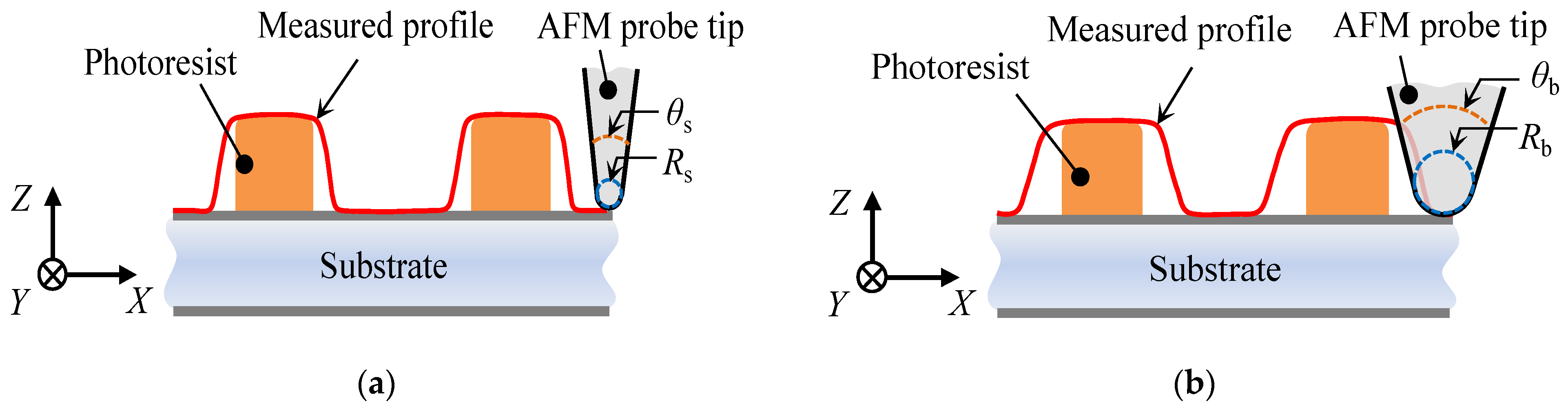
2.1. Principle for AFM Measurement of a Diffraction Grating with a Rectangular Profile

Figure 1 displays an illustration of a diffraction grating which was scanned using an AFM in the contact mode. A diffraction grating with a rectangular profile could be produced by combining the exposure and etching processes [7]. The resulting sidewalls are nearly perpendicular to the substrate’s surface, and the corner rounding in the intersection between the top surface and sidewalls is typically evaluated to be around several to ten nanometers [20]. Schematic diagrams of AFM measurements of a diffraction grating using different types of AFM probe tips can be seen in Figure 1a,b. The accuracy of diffraction grating measurements is significantly influenced by the tip shape of the AFM probe, including the tip radius and included angle, since the measured 3D AFM image is treated as a convolution of the diffraction grating surface and the AFM tip shape, according to [14]. Hence, it is crucial to reconstruct the 3D profile of a diffraction grating without considering the tip shape of the AFM probe to improve the accuracy of AFM measurements.
A grid with a corner-rounding radius of Rcorner and tilt angle α of sidewalls was extracted from the entire diffraction grating for further research. An AFM probe with a tip radius of Rtip and an included angle of θ (θ1 + θ2) was employed to scan the surface of the extracted grid. It was assumed that the AFM probe tip has a spherical shape, which can fit most AFM cantilevers. Figure 2 illustrates the geometric relationship between the measured and actual profiles of the grid in the cross-section. The measured profile of the grid in the cross-section is considered to be the convolution of the AFM tip shape and the actual profile of the measured surface due to the finite tip shape of the AFM probe. The tilt angles ε1 and ε2 of the measured profile on the sidewalls matched the corresponding tilt angles θ1 and θ2 of the AFM tip shape. This convolution of the geometries between the AFM tip shape and the actual profile of the grid results in the AFM image measurements of the right and left side of the grid in regions C1C3′ and C4C6′ corresponding to the actual profile in regions C1C3 and C4C6. The coordinates of point A have been adjusted from (x1, z1) to (x1′, z1) due to the convolution effect of Rtip. Consequently, the actual curve C1C2 in region C1C3 of the grid has been replaced by the measured curve C1C2′. Similarly, the coordinates of point B and the right sidewall (Line C2C3) of the grating in region C1C3 have been altered to (x2′, z2) and Line C2′C3′ in the AFM image, respectively, owing to the convolution effect of the tip radius (Rtip) and the included angle (θ) of the AFM probe tip. Based on the geometric relationship in the convolution area on the right side, it is feasible to formulate a reconstruction model that counteracts the impact of the AFM tip shape by using the following equation:
x i = x i 2 + z i + R t i p 2 R t i p 2 z i 2 x i C 1 C 2 x i tan π 2 θ 1 4 · R t i p + z i · tan θ 1 tan α 1 x i C 2 C 3
where (xi, zi) represents the coordinates of points in the region C1C3 and (xi′, zi) represents the corresponding coordinates of points in the region C1C3′. θ1 and α1 represent the inclined angle of the AFM tip shape on the left side and the tilt angle of the actual profile image on the right sidewall, respectively.
Similarly, the reconstruction model on the left side can be established using the same methodology and can be articulated as follows:
x j = x j 2 + z j + R t i p 2 R t i p 2 z j 2 x j C 4 C 5 x j + tan π 2 θ 2 4 · R t i p + z j tan θ 2 tan α 2 x j C 5 C 6
where (xj, zj) represents the coordinates of points in the region C4C5 and (xj′, zj) represents the corresponding coordinates of points in the region C4C5′. θ2 and α2 represent the inclined angle of the AFM tip shape on the right side and the tilt angle of the actual profile image on the left sidewall, respectively. The derivations of the reconstruction model can be found in Appendix A.
As explained above, the accuracy of the AFM measurement is significantly affected by the geometry of the AFM probe tip, including its tip radius and included angle. As a result, it is crucial to quantitatively estimate the tip radius and included angle of the AFM probe to eliminate the convolution effect in the AFM image. It is possible to evaluate the included angle of the AFM probe by scanning a line pattern structure [27]. However, accurately evaluating the tip radius of the AFM probe, which typically ranges in the nanometer scale, poses a challenge using conventional methods. Therefore, an edge reversal method is proposed to accurately assure the tip radius of the AFM probe in this paper [28].

2.2. Method for Evaluating the Geometry of an AFM Probe Tip

As explained in Section 2.1, it is not possible to accurately evaluate the geometry of an AFM probe tip by only scanning a reference artefact with steep sidewalls, as the radius of the AFM tip is too small for accurate measurement using this method. Hence, the assessment of an AFM probe tip’s geometry is divided into two parts. Firstly, the included angle θ of the AFM probe is assessed through the measurement of an artifact with a known topography. Secondly, the tip radius Rtip of the AFM probe is assessed using the edge reversal method.
Figure 2 illustrates that the convolution effect of the AFM probe causes the radius Rmea of the corner rounding to exceed the radius Rcorner of the artifact. Moreover, the edge slopes ε1 and ε2 of the measured profiles deviate from the actual edge slopes α1 and α2 of the standard artifact. Denoting the inclined angles of the left and right surfaces of the AFM probe as θ1 and θ2, respectively, the following equation is satisfied:
θ = θ 1 + θ 2 = ε 1 + ε 2
since ε1 > α1 and ε2 > α2, the included angle θ of the AFM probe can be determined by extracting ε1 and ε2 from the measured profile.
Quantitatively evaluating the AFM tip radius Rtip, which typically has a nominal value of several nanometers, poses a challenge compared to the measurement method for θ. The proposed solution to this issue is the edge reversal method [28,30]. The proposed method is designed in such a way that the AFM image of an object has an edge whose apex radius is comparable to the AFM tip radius and that of the indentation mark generated by using the edge of the object. Through the arithmetic operation with the obtained AFM images, the AFM tip radius can be evaluated quantitatively while separating the influence of the apex radius of the edge of the object.
Figure 3a,b show the schematic of the principle of the edge reversal method in the measurement of the indentation mark and the diamond tool (a single-point diamond tool was selected as the object of this study), respectively. The AFM tip radius can be evaluated with Equation (4) if the effect of elastic recovery on the indentation mark can be ignored [31,32]:
R t i p = R t o o l _ m R m a r k _ m 2
where Rtool_m and Rmark_m represent the measured apex radius of the indentation mark and measured cutting edge radius of the diamond tool, respectively. A description of the edge reversal method in detail can be found in the relevant papers [28,33]. As described above, the procedure of evaluating the tip shape of the AFM probe is complex and takes a lot of time in a single measurement. Simplification of this method will be researched in the future.

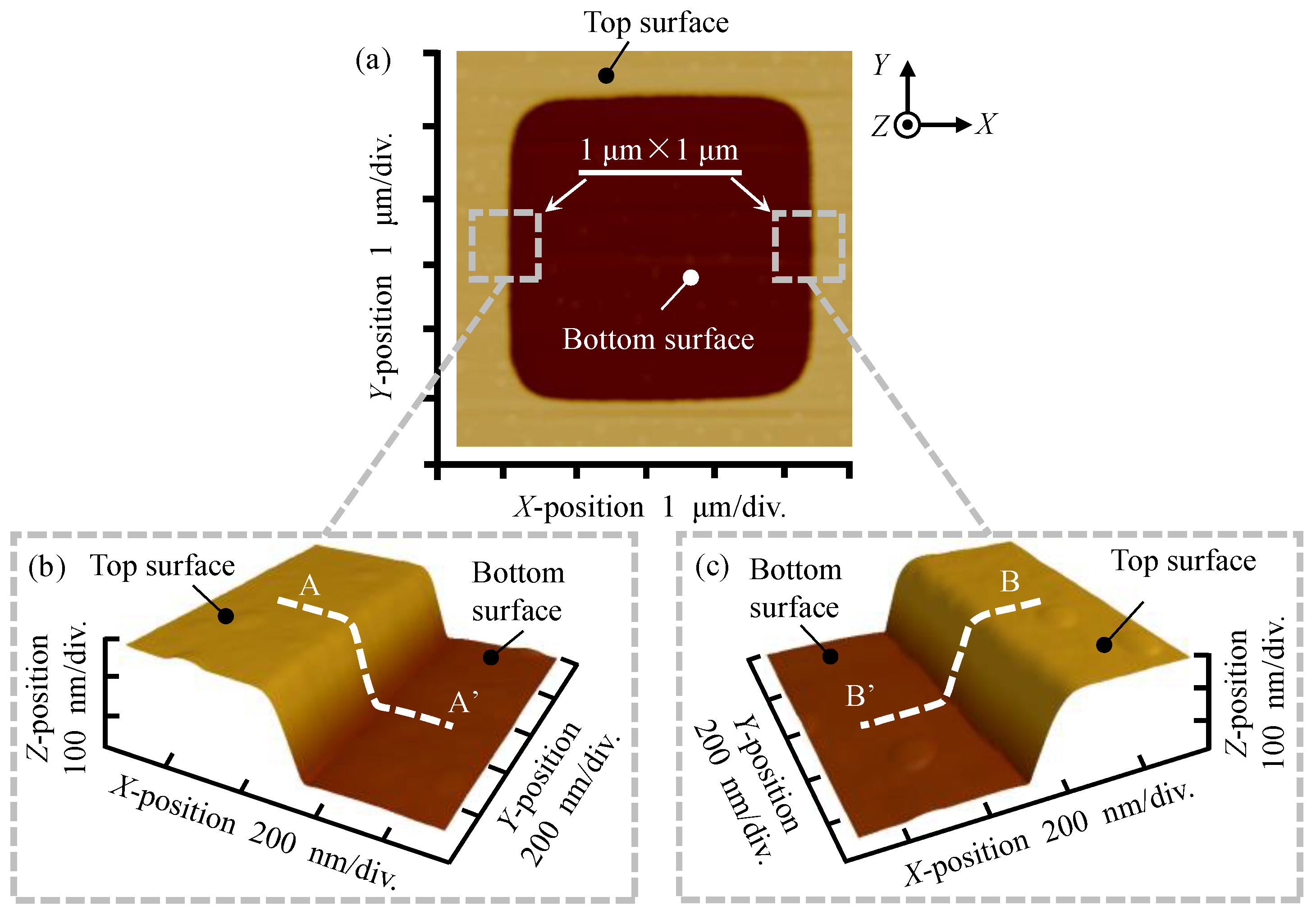
3. Experimental Results and Discussion

A series of experiments was carried out to verify the effectiveness of the proposed methods. A commercial two-dimensional (2D) diffraction grating (7110-00, Vecco, New York, NY, USA), which was fabricated using photolithography technology and has a nominal step height of 200 nm and pitch of 10 μm, was selected as the sample in this study. The SEM image of the diffraction grating is shown in Figure 4. The AFM image of the diffraction grating in the X-direction was reconstructed after obtaining the θ and Rtip of the AFM probe.

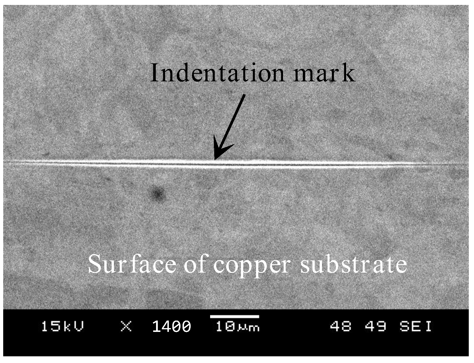
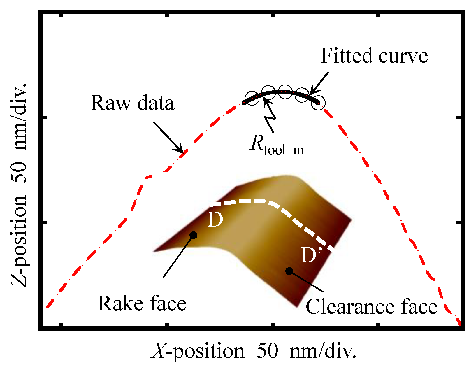
3.1. Evaluation of the Included Angle of the AFM Probe

The diffraction grating was also regarded as an artifact to evaluate the included angle θ of the AFM probe tip, since its sidewalls are almost perpendicular to the substrate. An AFM cantilever (OMCL-AC240TS, Olympus, Tokyo, Japan) with a nominal included angle of 36° and a nominal tip radius of 7 nm was employed to measure the topography of the diffraction grating on a commercial AFM instrument (Innova, Bruker, Billerica, MA, USA). The alignment between the diffraction grating and the AFM probe was meticulously carried out using an optical microscope to guarantee that the scan trace of the AFM probe was perpendicular to the sidewall of the diffraction grating in the X-direction, making it possible to accurately evaluate the included angle of the AFM probe. The scanning area was set to 10 μm × 10 μm with a scanning rate of 4 μm/s. Both the X- and Y-directions had 1024 scanning lines.
The measured AFM image of the diffraction grating is shown in Figure 5a. The enlarged 3D AFM images with an area of 1 μm × 1 μm on the left and the right sides are shown in Figure 5b,c, respectively. The sectional profiles on A-A′ and B-B′ extracted from the left and right sides of the 3D AFM image to estimate the included angle are shown in Figure 6a,b, respectively. The sidewalls on the left and right side show a slight slope, which is due to the geometry of the AFM probe. Tilt angles (ε1 and ε2) were obtained by fitting points in the sidewalls of the sectional profile using the least squares method. The values obtained for ε1 and ε2 of the diffraction grating were 19.02° and 18.45°, respectively. Substituting these values into Equation (3), the included angle θ of the AFM probe tip used during the measurement was calculated to be 37.47°. The estimated value was very close to the nominal value of 36° given by the manufacturer, which effectively demonstrated the estimation of θ for the AFM tip. Moreover, the measured corner radii on the left (Rmea_L) and right (Rmea_R) sides were found to be 54.24 nm and 78.37 nm, respectively.

3.2. Evaluation of the Tip Radius of the AFM Probe

Prior to using the AFM to measure the topography of the indentation mark and the diamond tool, an ultra-precision nanoindentation instrument was designed to accurately replicate the geometry of the cutting edge of a diamond tool with a nominal nose radius of 1 mm onto a soft copper substrate by indenting the copper substrate with the diamond tool [30]. The quality of the replicated indentation mark can be affected by the surface roughness of the workpiece. To minimize this influence, a workpiece with an RMS roughness of 2.43 nm was used in the experiments. Figure 7 shows the SEM image of the indentation mark. The results obtained by molecular dynamics (MD) simulations indicated that elastic recovery of the indentation mark can be ignored when the indentation depth is greater than 200 nm. The principle of the ultra-precision nanoindentation instrument and the procedure for creating the indentation mark can be found in references [30,33] and will not be repeated in this paper for the sake of brevity.
The AFM cantilever previously utilized for measuring the diffraction grating as described in Section 3.1 was also employed to measure the 3D profiles of the indentation mark and diamond tool. The indentation mark was initially scanned at a rate of 0.8 μm/s with a scanning area of 2 μm (X) × 2 μm (Y). The number of scanning lines was set to 1024 in both the X- and Y-directions. Figure 8 shows the 3D AFM image and the cross-sectional profile extracted from the AFM image of the replicated artifact with an area of 0.4 μm × 0.4 μm. The apex radius of the indentation mark was obtained by fitting the points in the apex of the cross-sectional profile of the indentation mark using the least squares method. The radius of the fitted arc Rmark_m, which is represented by a black solid line with circle markers in Figure 8, is approximately 17.08 nm.
The diamond tool was mounted on a tool holder and positioned on the Z-scanner of the AFM instrument. The bisector of the included angle of the diamond tool, between its rake face and clearance face, was aligned parallel to the Z-direction of the AFM. Subsequently, the diamond tool was scanned with the same AFM tip, using the same parameters as in the measurement of the indentation mark, including the scan rate, the scan area and the number of data points in the X- and Y-directions.
Figure 9 shows the 3D AFM image and cross-sectional profile extracted from the AFM image of the diamond tool, covering an area of 0.4 μm × 0.4 μm. A discernible edge separates the rake face and the clearance face, which can be useful for determining Rtool_m. The radius of the fitted arc, Rtool_m, indicating the apex radius of the cutting edge, was calculated to be approximately 32.19 nm using the least squares method. Therefore, Rtip was evaluated to be approximately 7.55 nm by substituting the evaluated Rmark_m and Rtool_m into Equation (4). The evaluated Rtip corresponded well to the nominal Rtip of 7 nm.
The experimental results above demonstrate that accurate characterization of the geometry of the tip radius and included angle of the AFM probe tip on-machine can be achieved through the edge reversal method and scanning of a line pattern structure, respectively. Please note that the measured parameters of the selected AFM cantilever with a triangular pyramid structure can only reflect the outline of the AFM tip shape in contact with the sample surface during the measurement. There will be a slight difference in the AFM profile images of the scanned sample if the alignment between the AFM cantilever and sample is altered prior to the AFM measurement.

3.3. Reconstruction of 3D AFM Image of the Diffraction Grating

As mentioned above, the geometry of the AFM probe tip, including Rtip and θ, can significantly influence the measurement accuracy of the grating of an AFM. After Rtip and θ were obtained, the topography convolutions induced by the AFM probe tip in the 3D topographic characterization of the diffraction grating were corrected using the proposed reconstruction model.
Figure 10a,b depict the reconstructed 3D AFM images of the diffraction grating on the right and left sides, respectively, corresponding to the 3D AFM images exhibited in Figure 5b,c. Both the top and bottom surfaces of the reconstructed 3D image can be clearly seen from Figure 10a,b. A significant decrease in the inclined angle of the sidewall can be observed when compared to Figure 5b,c. This is because the lateral resolution of the white light interferometer used to measure the actual surface profile of the diffraction is too large, reaching several hundred nanometers and exceeding the requirement of several nanometers in lateral resolution to measure the sidewall and corner rounding in the X-axis direction. Currently, there is no effective method in our laboratory that can measure the actual profile image of the diffraction grating. A comparison between the reconstructed and actual profile images of the grating based on a designed standard artefact will be carried out in the future.
The cross-sectional profiles extracted from Figure 10 are shown in Figure 11. It is apparent from Figure 11 that both sidewalls became vertical, and the corner radii decreased. The reconstructed corner radius (Rrec_L) on the left side was found to be 46.70 nm, while that on the right side (Rrec_R) was 70.86 nm. The differences of the reconstructed and the measured corner radii on both left and right sides were calculated to be 7.54 nm and 7.51 nm, respectively. These values were almost the same as those of the measured tip radius of the AFM probe. The tilt angles of the sidewalls on the left and right sides were both reconstructed to be zero, which corresponded well with the assumed tilt angle of the sidewalls in this experiment. The sectional profiles without reconstruction were additionally plotted in Figure 11 for comparison. It is evident that the influence of the tip radius (Rtip) and included angle (θ) of the AFM cantilever was successfully removed, thus demonstrating the feasibility of the proposed reconstruction model. Please note that the actual tilt angle of the sidewall can be evaluated using a CD-AFM or CNT-AFM. However, the purpose of this research is to verify the feasibility of the proposed reconstruction method for compensating the profile convolutions induced by the tip shape of the AFM probe in the measurement of a diffraction grating. Therefore, we assume that the sidewall is perpendicular to the substrate before reconstruction.
Figure 12 presents the corner radius values of the reconstructed AFM image of the diffraction grating in ten distinct sections. It can be seen that the corrected corner radii were smaller than the measured corner radii. The differences between the measured and the corrected corner radii on the left and right sides were evaluated to be 7.544 nm with a standard deviation of 0.018 nm and 7.534 nm with a standard deviation of 0.013 nm, respectively. The obtained values were close to that of the AFM tip radius of 7.55 nm, which was determined through the edge reversal method. The proposed reconstruction method compensated for twenty cross-sections in the 3D image. It was able to accurately reconstruct the tilt angle and corner radius in each cross-section. Therefore, the repeatability of the proposed reconstruction method can be confirmed with the above results.

4. Conclusions

A method of reconstruction has been proposed with the objective of removing the impact of the geometry convolution of the AFM probe tip on the scanned AFM image of a rectangular diffraction grating. The geometry of the AFM probe tip has been assessed through the edge reversal method and a commercial diffraction grating, resulting in a tip radius of 7.55 nm and an included angle of 37.47 degrees. The measured results corresponded well with the nominal geometry of the AFM probe tip provided by the manufacturer. The diffraction grating was also used as a scanned sample, and its 3D AFM image was reconstructed using the proposed model. The corner radii at the left and right sides (Rmea_L and Rmea_R, respectively) of the diffraction grating were assessed to be 54.24 nm and 78.37 nm before reconstruction. A tilt angle was observed in the measured sidewall of the diffraction grating. Following the reconstruction process, the values for Rrec_L and Rrec_R were adjusted to 46.70 nm and 70.86 nm, respectively, while the tilt angles were determined to be zero. This provides evidence for the validity of the proposed reconstruction model. Experimental results have confirmed that the influence of the geometry of the AFM probe tip on the 3D AFM image of the diffraction grating can be successfully eliminated using the proposed reconstruction method.

Author Contributions

Conceptualization, Methodology, Validation, Visualization and Writing: K.Z.; Supervision and Review: Y.B.; Supervision and Review: Z.Z. All authors have read and agreed to the published version of the manuscript.

Funding

This work is supported by the Japanese Government Scholarship (MEXT), the China Scholarship Council (CSC), the Fundamental Research Fund of National Institute of Metrology, China (Grant No. AKYCX2302), China National Key Research and Development Plan (Grant No. 2021YFF0603803) and the National Natural Science Foundation of China (Grant No. 52175527).

Data Availability Statement

Data and optimization codes can be shared upon request.

Acknowledgments

We thank Wei Gao (Tohoku University) for kindly supporting the related experiments, Yuki Shimizu (Hokkaido University) for general discussions related to visualization and Yindi Cai (Dalian University of Technology) for careful advice on the manuscript.

Conflicts of Interest

The authors declare no conflicts of interest.

Appendix A

An AFM probe with a tip radius of Rtip and an included angle of θ (θ1 + θ2) is utilized to scan the surface of the diffraction grating. As shown in Figure A1, due to the finite tip shape of the AFM probe, the measured profile image of the diffraction grating in the cross-section is considered as the convolution of the tip shape of the AFM probe and the actual profile of the measured surface. The measured profile image in the convolution region from C1 to C3 can be classified into two sections based on the geometrical relationship. In the curve region between C1 and C2, the measured profile image is only affected by the tip radius of the AFM probe. The coordinates of point A1 on the actual surface of the diffraction grating are denoted as (x1, z) while the coordinates of point A2 in the measured profile image are denoted as (x1′, z1). According to the geometrical relationship between the actual and the measured profiles, the following equations can be derived:
x 1 = R c o r n e r 2 z 2
R m e a = R c o r n e r + R t i p = x 1 2 + ( z + R t i p ) 2
The X-coordinates of point A1 can be expressed as follows by combining the above equations:
x i = x i 2 + z i + R t i p 2 R t i p 2 z i 2 x i C 1 C 2
In the straight-line region from C2 to C3, the measured profile is affected by the tip radius and the included angle of the AFM probe. The coordinates of point B1 on the actual surface of the diffraction grating are denoted as (x2, z) while the coordinates of point B3 in the measured profile image are denoted as (x2′, z1). According to the geometrical relationship between the actual and the measured profiles, the following equations can be derived:
x 2 = x 2 tan π 2 θ 1 4 · R t i p
x 2 = x 2 z · ( tan θ 1 tan α 1 )
The X-coordinates of point B1 can be expressed as follows by combining the above equations:
x i = x i tan π 2 θ 1 4 · R t i p + z i tan θ 1 tan α 1 x i C 2 C 3
where θ1 and α1 represent the inclined angle of the AFM tip shape on the left side and the tilt angle of the actual profile image on the right sidewall, respectively.
Figure A1. The geometrical relationship between the measured and the actual profiles of the diffraction grating scanned by an AFM probe tip.
Machines 12 00126 g0a1

References

  1. Yan, J.-N.; Chang, C.-W.; Lee, Y.-C. A metal-embedded photo-mask for contact photolithography with application on patterned sapphire substrate. Microelectron. Eng. 2014, 122, 20–24. [Google Scholar] [CrossRef]
  2. Gao, W. Precision Nanometrology–Sensors and Measuring Systems for Nanomanufacturing; Springer: London, UK, 2010. [Google Scholar]
  3. Li, X.; Gao, W.; Muto, H.; Shimizu, Y.; Ito, S.; Dian, S. A six-degree-of-freedom surface encoder for precision positioning of a planar motion stage. Precis. Eng. 2013, 37, 771–781. [Google Scholar] [CrossRef]
  4. Gao, W.; Haitjema, H.; Fang, F.; Leach, R.; Cheung, C.; Savio, E.; Linares, J. On-machine and in-process surface metrology for precision manufacturing. CIRP Ann. 2019, 68, 843–866. [Google Scholar] [CrossRef]
  5. Quan, L.; Shimizu, Y.; Xiong, X.; Matsukuma, H.; Gao, W. A new method for evaluation of the pitch deviation of a linear scale grating by an optical angle sensor. Precis. Eng. 2021, 67, 1–13. [Google Scholar] [CrossRef]
  6. Shimizu, Y.; Uehara, K.; Matsukuma, H.; Gao, W. Evaluation of the grating period based on laser diffraction by using a mode-locked femtosecond laser beam. J. Adv. Mech. Des. Syst. Manuf. 2018, 12, JAMDSM0097. [Google Scholar] [CrossRef]
  7. Yu, Z.; Chen, L.; Wu, W.; Ge, H.; Chou, S.Y. Fabrication of nanoscale gratings with reduced line edge roughness using nanoimprint lithography. J. Vac. Sci. Technol. B Microelectron. Nanometer Struct. Process. Meas. Phenom. 2003, 21, 2089–2092. [Google Scholar] [CrossRef]
  8. Shin, D.W.; Quan, L.; Shimizu, Y.; Matsukuma, H.; Cai, Y.; Manske, E.; Gao, W. In-Situ Evaluation of the Pitch of a Reflective-Type Scale Grating by Using a Mode-Locked Femtosecond Laser. Appl. Sci. 2021, 11, 8028. [Google Scholar] [CrossRef]
  9. Dai, G.; Koenders, L.; Pohlenz, F.; Dziomba, T.; Danzebrink, H.-U. Accurate and traceable calibration of one-dimensional gratings. Meas. Sci. Technol. 2005, 16, 1241–1249. [Google Scholar] [CrossRef]
  10. Dai, G.; Pohlenz, F.; Dziomba, T.; Xu, M.; Diener, A.; Koenders, L.; Danzebrink, H.-U. Accurate and traceable calibration of two-dimensional gratings. Meas. Sci. Technol. 2007, 18, 415–421. [Google Scholar] [CrossRef]
  11. Gao, W.; Asai, T.; Arai, Y. Precision and fast measurement of 3D cutting edge profiles of single point diamond micro-tools. CIRP Ann.-Manuf. Technol. 2009, 58, 451–454. [Google Scholar] [CrossRef]
  12. Itoh, H.; Fujimoto, T.; Ichimura, S. Tip characterizer for atomic force microscopy. Rev. Sci. Instrum. 2006, 77, 103704. [Google Scholar] [CrossRef]
  13. Villarrubia, J. Algorithms for scanned probe microscope image simulation, surface reconstruction, and tip estimation. J. Res. Natl. Inst. Stand. Technol. 1997, 102, 425–454. [Google Scholar] [CrossRef]
  14. Dongmo, L.; Villarrubia, J.; Jones, S.; Renegar, T.; Postek, M.; Song, J. Experimental test of blind tip reconstruction for scanning probe microscopy. Ultramicroscopy 2000, 85, 141–153. [Google Scholar] [CrossRef]
  15. Orji, N.G.; Dixson, R.G. Higher order tip effects in traceable CD-AFM-based linewidth measurements. Meas. Sci. Technol. 2007, 18, 448–455. [Google Scholar] [CrossRef]
  16. Nguyen, C.V.; Ye, Q.; Meyyappan, M. Carbon nanotube tips for scanning probe microscopy: Fabrication and high aspect ratio nanometrology. Meas. Sci. Technol. 2005, 16, 2138–2146. [Google Scholar] [CrossRef]
  17. Dai, H.; Hafner, J.H.; Rinzler, A.G.; Colbert, D.T.; Smalley, R.E. Nanotubes as nanoprobes in scanning probe microscopy. Nature 1996, 384, 147–150. [Google Scholar] [CrossRef]
  18. Martin, Y.; Wickramasinghe, H.K. Method for imaging sidewalls by atomic force microscopy. Appl. Phys. Lett. 1994, 64, 2498–2500. [Google Scholar] [CrossRef]
  19. Dahlen, G.; Osborn, M.; Liu, H.-C.; Jain, R.; Foreman, W.; Osborne, J.R. Critical dimension AFM tip characterization and image reconstruction applied to the 45-nm node. In Proceedings of the SPIE 31st International Symposium on Advanced Lithography, San Jose, CA, USA, 19–24 February 2006; Volume 6152, pp. 945–955. [Google Scholar]
  20. Hussain, D.; Ahmad, K.; Song, J.; Xie, H. Advances in the atomic force microscopy for critical dimension metrology. Meas. Sci. Technol. 2016, 28, 012001. [Google Scholar] [CrossRef]
  21. Bykov, V.; Novikov, Y.; Rakov, A.; Shikin, S. Defining the parameters of a cantilever tip AFM by reference structure. Ultramicroscopy 2003, 96, 175–180. [Google Scholar] [CrossRef]
  22. Vesenka, J.; Miller, R.; Henderson, E. Three-dimensional probe reconstruction for atomic force microscopy. Rev. Sci. Instrum. 1994, 65, 2249–2251. [Google Scholar] [CrossRef]
  23. Yue, X.; Lei, D.; Cui, H.; Zhang, X.; Xu, M.; Kong, L. An integrated method for measurement of diamond tools based on AFM. Precis. Eng. 2017, 50, 132–141. [Google Scholar] [CrossRef]
  24. Liu, J.; Notbohm, J.K.; Carpick, R.W.; Turner, K.T. Method for Characterizing Nanoscale Wear of Atomic Force Microscope Tips. ACS Nano 2010, 4, 3763–3772. [Google Scholar] [CrossRef] [PubMed]
  25. Chen, L.; Cheung, C.L.; Ashby, P.D.; Lieber, C.M. Single-Walled Carbon Nanotube AFM Probes: Optimal Imaging Resolution of Nanoclusters and Biomolecules in Ambient and Fluid Environments. Nano Lett. 2004, 4, 1725–1731. [Google Scholar] [CrossRef]
  26. Chen, Z.; Luo, J.; Doudevski, I.; Erten, S.; Kim, S.H. Atomic Force Microscopy (AFM) Analysis of an Object Larger and Sharper than the AFM Tip. Microsc. Microanal. 2019, 25, 1106–1111. [Google Scholar] [CrossRef]
  27. Morgenroth, W.; Meyer, H.; Sulzbach, T.; Brendel, B.; Hübner, U.; Mirandé, W. Downwards to metrology in nanoscale: Determination of the AFM tip shape with well-known sharp-edged calibration structures. Appl. Phys. A Mater. Sci. Process. 2003, 76, 913–917. [Google Scholar] [CrossRef]
  28. Chen, Y.-L.; Cai, Y.; Xu, M.; Shimizu, Y.; Ito, S.; Gao, W. An edge reversal method for precision measurement of cutting edge radius of single point diamond tools. Precis. Eng. 2017, 50, 380–387. [Google Scholar] [CrossRef]
  29. Zhang, K.; Shimizu, Y.; Matsukuma, H.; Cai, Y.; Gao, W. An application of the edge reversal method for accurate reconstruction of the three-dimensional profile of a single-point diamond tool obtained by an atomic force microscope. Int. J. Adv. Manuf. Technol. 2021, 117, 2883–2893. [Google Scholar] [CrossRef]
  30. Cai, Y.; Chen, Y.-L.; Xu, M.; Shimizu, Y.; Ito, S.; Matsukuma, H.; Gao, W. An ultra-precision tool nanoindentation instrument for replication of single point diamond tool cutting edges. Meas. Sci. Technol. 2018, 29, 054004. [Google Scholar] [CrossRef]
  31. Cai, Y.; Chen, Y.-L.; Shimizu, Y.; Ito, S.; Gao, W. Molecular dynamics simulation of elastic–plastic deformation associated with tool–workpiece contact in force sensor–integrated fast tool servo. Proc. Inst. Mech. Eng. Part B J. Eng. Manuf. 2018, 232, 1893–1902. [Google Scholar] [CrossRef]
  32. Cai, Y.; Chen, Y.-L.; Shimizu, Y.; Ito, S.; Gao, W.; Zhang, L. Molecular dynamics simulation of subnanometric tool-workpiece contact on a force sensor-integrated fast tool servo for ultra-precision microcutting. Appl. Surf. Sci. 2016, 369, 354–365. [Google Scholar] [CrossRef]
  33. Zhang, K.; Cai, Y.; Shimizu, Y.; Matsukuma, H.; Gao, W. High-Precision Cutting Edge Radius Measurement of Single Point Diamond Tools Using an Atomic Force Microscope and a Reverse Cutting Edge Artifact. Appl. Sci. 2020, 10, 4799. [Google Scholar] [CrossRef]
Figure 1. AFM measurement of a diffraction grating with rectangular profiles. (a) The trajectory of the tip apex of the AFM probe with high resolution (utilization of an AFM probe with a tip radius of Rs and an included angle of θs); (b) the trajectory of the tip apex of the AFM probe with low resolution (utilization of an AFM probe with a tip radius of Rb and an included angle of θb, where Rb > Rs and θb > θs).
Machines 12 00126 g001
Figure 2. The schematic of the geometrical relationship between the measured profile image and the real surface of a grid.
Machines 12 00126 g002
Figure 3. Principle of the edge reversal method for evaluating the tip radius of an AFM probe. (a) Trajectory of the AFM tip apex in the measurement of the indentation mark in the cross-section; (b) trajectory of the AFM tip apex in the measurement of the diamond tool in the cross-section.
Machines 12 00126 g003
Figure 4. Top view of the SEM image of a commercial diffraction grating.
Machines 12 00126 g004
Figure 5. A 3D AFM image of the diffraction grating. (a) Top view; (b) enlarged 3D AFM image on the left side and (c) enlarged 3D AFM image on the right side.
Machines 12 00126 g005
Figure 6. Sectional profiles of the 3D AFM image: (a) A-A′ on the left side and (b) B-B′ on the right side.
Machines 12 00126 g006
Figure 7. SEM image of the indentation mark replicated using the designed nanoindentation instrument.
Machines 12 00126 g007
Figure 8. The apex radius (Rmark_m) achieved from section C-C′ of the AFM topography of the indentation mark.
Machines 12 00126 g008
Figure 9. The apex radius (Rtool_m) achieved from section D-D′ of the AFM topography of the diamond tool.
Machines 12 00126 g009
Figure 10. Reconstructed 3D AFM image of the diffraction grating on (a) the left side and (b) the right side.
Machines 12 00126 g010
Figure 11. Reconstructed sectional profiles of the diffraction grating on (a) the left side and (b) the right side.
Machines 12 00126 g011
Figure 12. Summarization of the corner radii of (a) the left side and (b) the right side of the reconstructed AFM image of the diffraction grating in ten different sections.
Machines 12 00126 g012
Disclaimer/Publisher’s Note: The statements, opinions and data contained in all publications are solely those of the individual author(s) and contributor(s) and not of MDPI and/or the editor(s). MDPI and/or the editor(s) disclaim responsibility for any injury to people or property resulting from any ideas, methods, instructions or products referred to in the content.

