Article

A Systematic Analysis of Printed Circuit Boards Bending during In-Circuit Tests

1
MEtRICs Research Centre, Guimarães, School of Engineering, University of Minho, 4800-058 Guimarães, Portugal
2
InsideLimits, Rua do Rodelo, 4400-569 Canidelo, Portugal
3
CMAT Research Centre, School of Sciences, University of Minho, 4800-058 Guimarães, Portugal
*
Author to whom correspondence should be addressed.
Machines 2022, 10(2), 135; https://doi.org/10.3390/machines10020135
Submission received: 31 December 2021 / Revised: 3 February 2022 / Accepted: 8 February 2022 / Published: 13 February 2022
(This article belongs to the Special Issue Feature Papers to Celebrate the First Impact Factor of Machines)

Abstract

:
When performing In-Circuit Tests (ICTs) of Printed Circuit Boards (PCBs), there are certain phenomena related with strain analysis that must be known in order to obtain stronger and more accurate testing results. During testing, PCBs are often subjected to mechanical bending efforts that induce excessive strain. This study focuses on the building of a Finite Elements Analysis (FEA) methodology that prevents excessive bending strain in critical points of a PCB during an ICT. To validate this methodology, a set of experimental tests, matched with a set of FEA, were carried out. Thus, companies, before the development of an ICT machine (fixture), will be able to use this FEA methodology to predict whether the maximum strain of a PCB under study, when subjected to its ICT, will damage it, thus reducing unnecessary production costs. A guideline was thus designed to enable the creation of the most representative Finite Elements Model (FEM) for any PCB, based on its amount and direction of copper traces.

1. Introduction

During the whole PCB production process, electronic devices are subjected to several external interferences that can cause excessive bending, damaging them. Several studies related to PCB bending have been carried out, trying to predict PCB behaviour during several phases of the production process, as well as when they are subjected to external efforts in their final usage.
One of the most common quality control processes PCBs are subjected to at the end of the production chain are the ICTs. During these tests, PCBs are positioned in a bed of nails and, by mean of pressers, are pressed against the bed. The pressers’ locations are achieved without carrying out any previous study, based only on the expertise of the ICT fixtures designers. This expertise-based process often leads to high bending efforts that induce an excessive strain on the PCB, damaging them, and causing failure in proper operation of the PCB [1].
Several studies have been performed to analyse mechanically the bending effects on PCBs. The greatest number of works have resorted to three- and four-point bending tests, and are addressed to the packages’ solder joints reliability and their main failure mechanisms [2,3,4,5,6,7,8,9,10,11]. There are also studies using drop-impact tests to understand the PCBs’ dynamic bending effects on solder joint behaviour [12,13]. Furthermore, there are some analyses regarding the effects of thermal bending on solder joints [14,15,16]. However, there is a lack of specific work and research on PCB bending during ICTs.
Therefore, this project is intended to build a guideline that allows to create the best FEM (the simplest and, at the same time, the most accurate) for any type of PCB, depending on their geometric and mechanical characteristics. This is an advantageous tool to ICT producing companies because before assembly of any ICT fixture and its pressers, it is possible to create an FEM to predict the strains each PCB would be subjected to during an ICT. It then allows the ICT fixture-designing teams to predict whether the strains at the critical points will be greater than the maximum allowable value and, if necessary, to change the pressers’ location in order to minimize strains. It is important to mention that this study focus on bare board ICTs if it does not deal with PCBAs, and that it can be used for Flying Probe ICTs since the load applied by the probe is known. In addition, it might be addressed to other applications during the PCB production process, as long as the PCBs are subjected to mechanical bending efforts due to supports and contact points.
In order to achieve the proposed goals, this paper is organized as follows: Section 1 introduces the root causes and the motivations for this paper, fitting the project into the current fierce evolution and competition in the mechatronics industry. A brief introduction of what an ICT is and its main limitations are provided. Thereafter, a study of the relevant state of the art is briefly exposed. Finally, the goals of the paper are presented and why this paper could be a great asset to the mechatronics industry, specially to the ICTs industry, is justified.
Section 2 presents the adopted materials and methods used to carry on with the project. First, the experimental setup is shown and explained. The machine that will emulate the conditions of an ICT machine, as well as its main components and operation mode, and the data acquisition devices and method, are shown. Further, based on studies already carried out by several authors, the way the FEA are going to be applied to the present study case are also presented. More concretely, the pre-processing phase and the used parameters are announced.
In Section 3, the results obtained in the previous chapter, from both experimental tests and numerical simulations, are provided.
The results’ analysis and discussion are provided in Section 4. The results from the experimental tests are assumed as the target results and, for that reason, the data resulting from the numerical simulations are compared with the experimental results. These results, regarding physical and mechanical representativeness, are discussed.
Finally, in Section 5, the conclusions are exposed. Based on these conclusions, as initially proposed, a methodology that prevents excessive bending strain is presented.

2. Materials and Methods

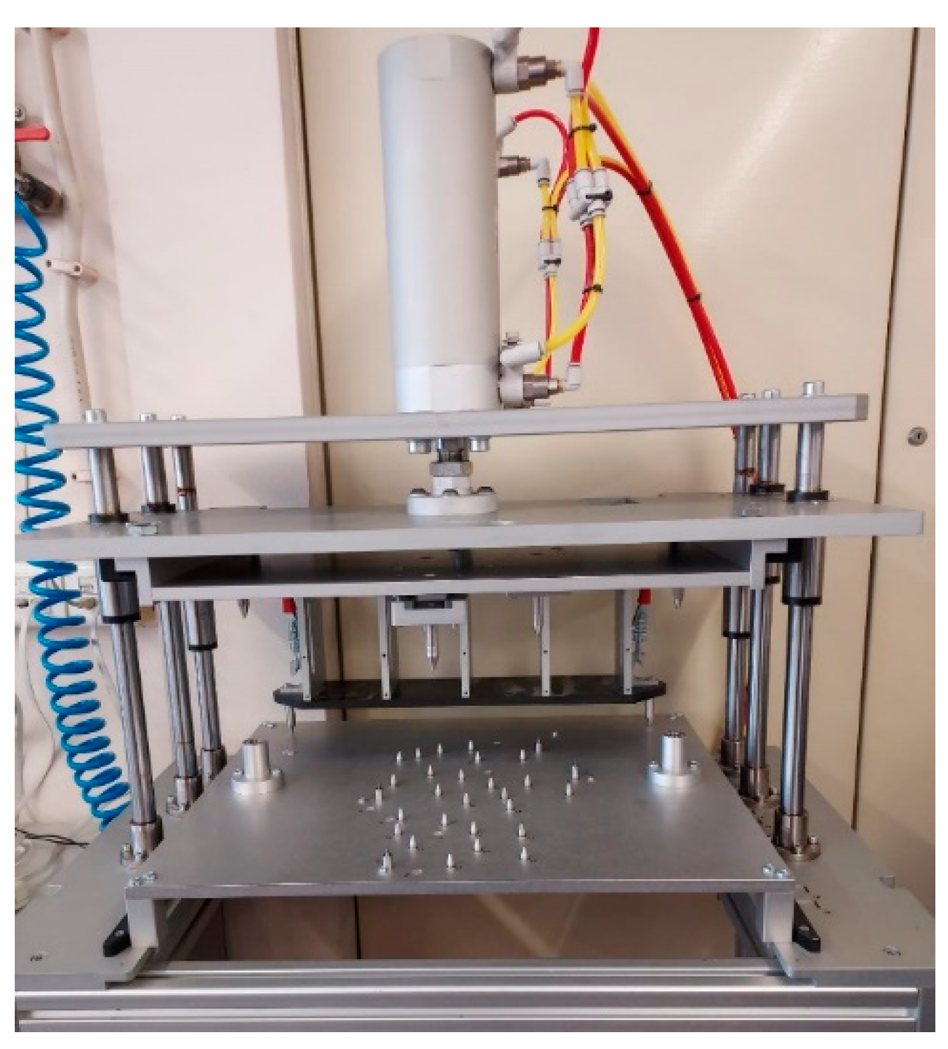
2.1. Experimental Setup

To emulate the conditions of an ICT machine, a set of experimental tests were performed in an adapted machine, presented in Figure 1.
The machine comprised of a pneumatic cylinder and bottom and upper plates. To apply force, the upper plate moves downward and meets the bottom plate, guiding each other with the help of a guiding system.
The PCB is placed on top of support pins that imitate needles and it is guided into the experimental machine using guiding pins with tight tolerance. In the guiding pins, the PCB is restricted in the Z axis (Figure 2).
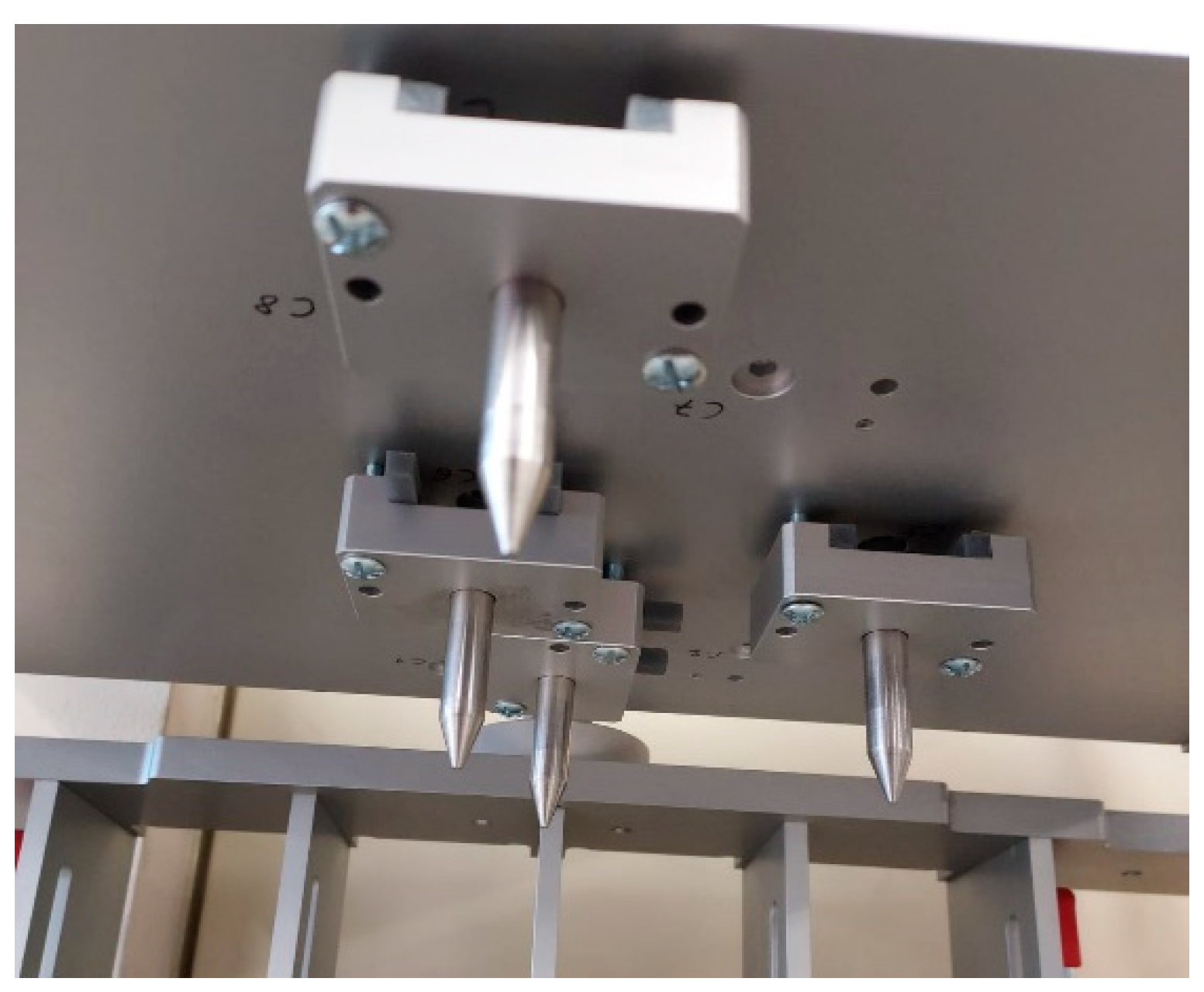
To apply load, pressers (as shown in Figure 3) were used. The geometry of the pressers is as it occurs in a real ICT.
For each presser, a load cell is associated to precisely quantify the force on every used presser.
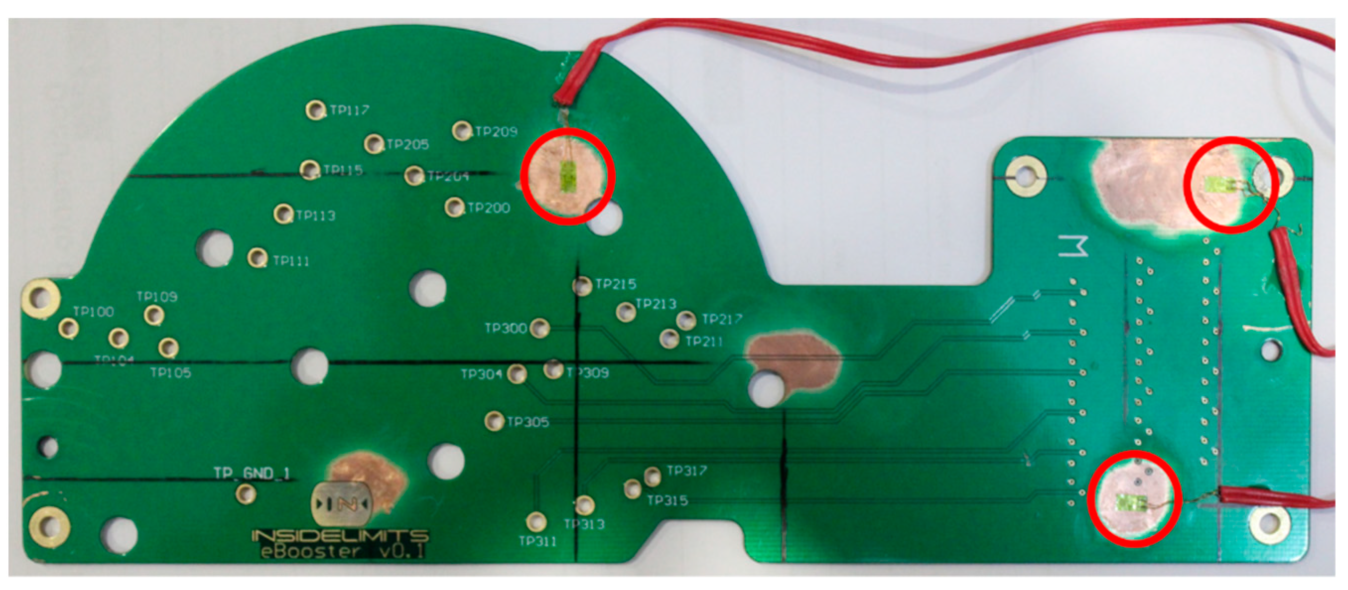
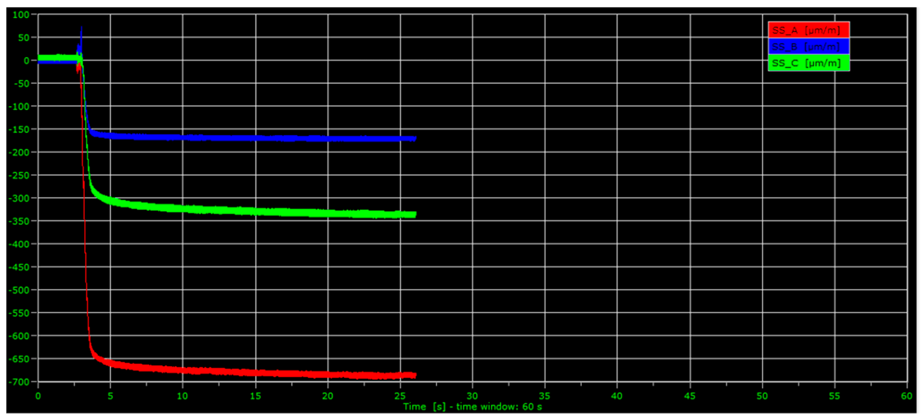
To measure the strain data for each experimental test, strain gages were used. This is the most practical way to find the strains without affecting the response of the measured part [4,6,7,8,10,14,17,
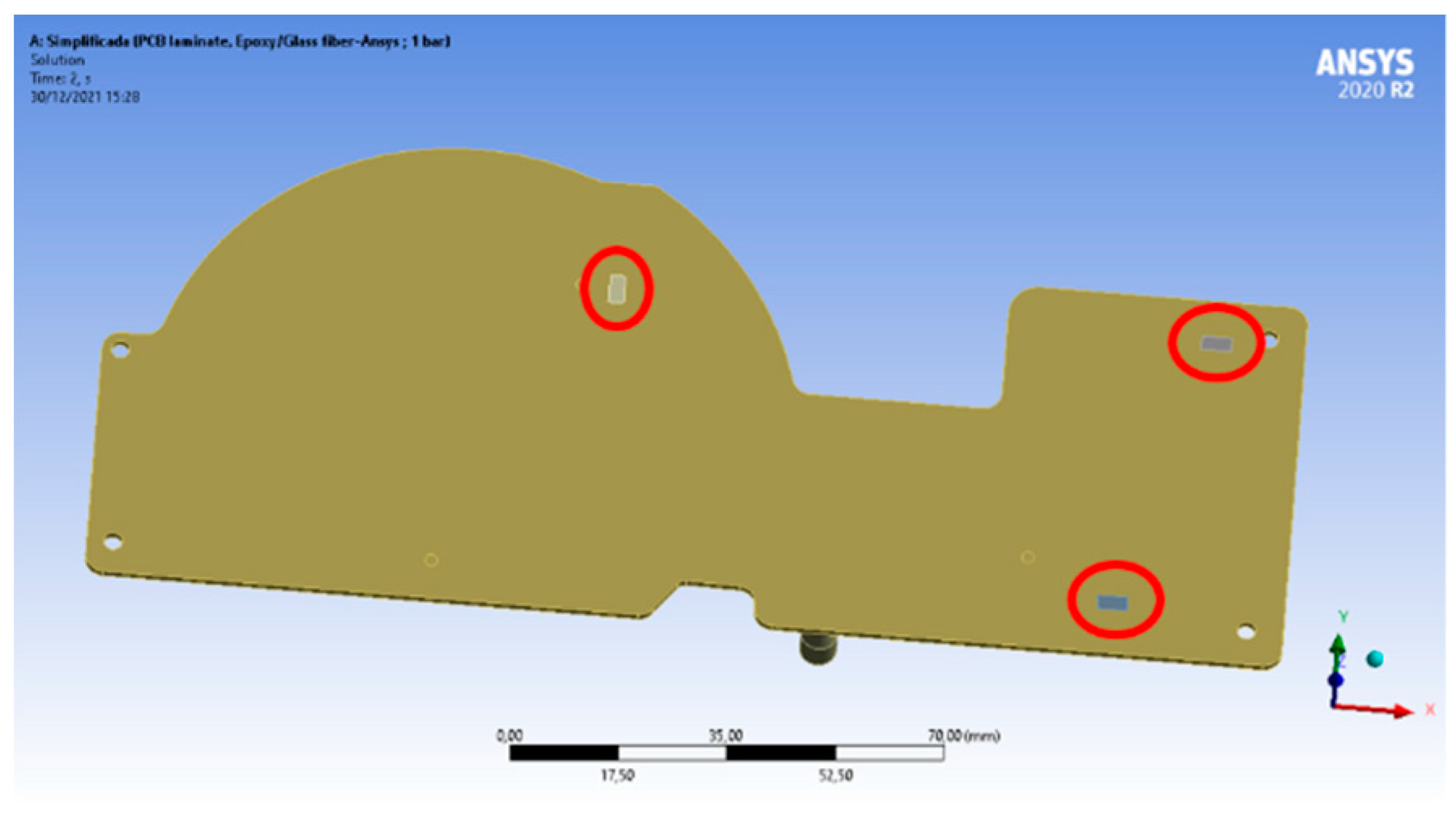
18]. Three uniaxial strain gages (KFGS-1-120-C1-23) were applied in strategic positions of the PCB (Figure 4). The strain gages are connected to the signal amplifier HBM QuantumX MX1615B which, in turn, are connected to a PC where the data is displayed.
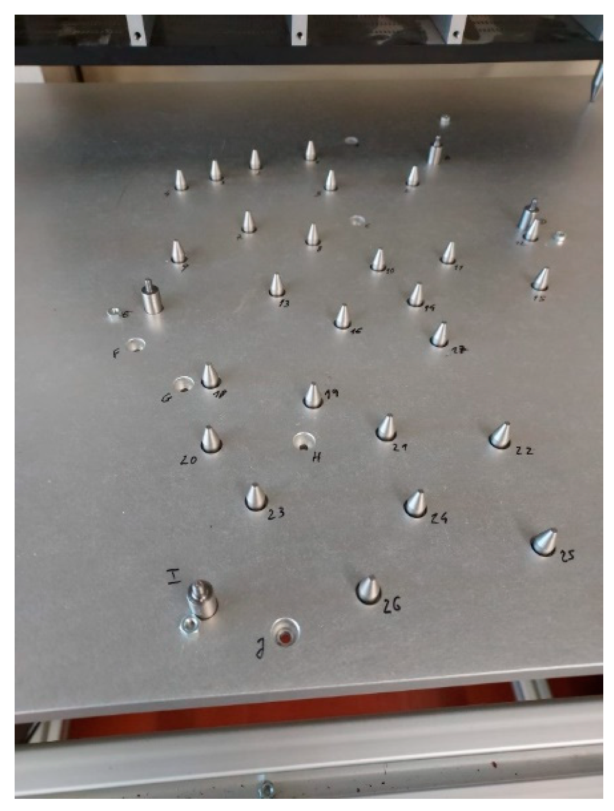
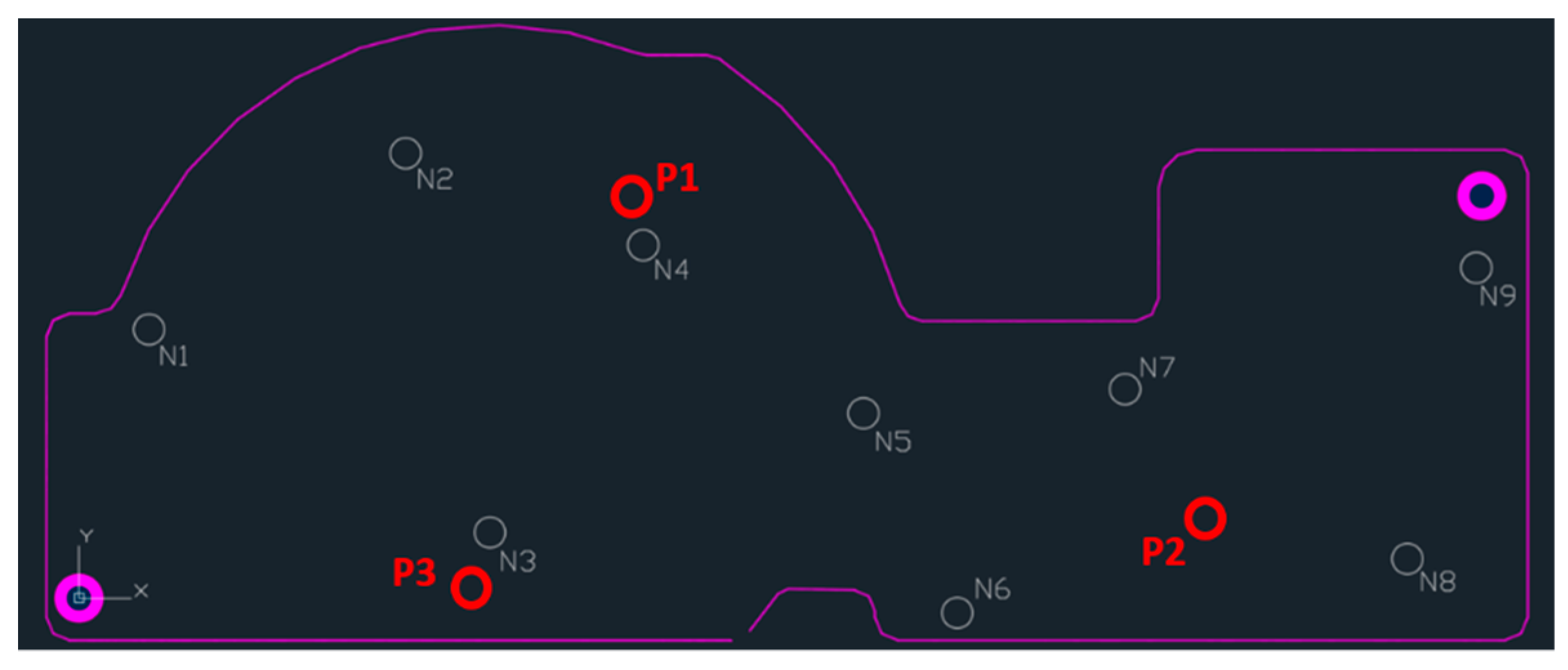
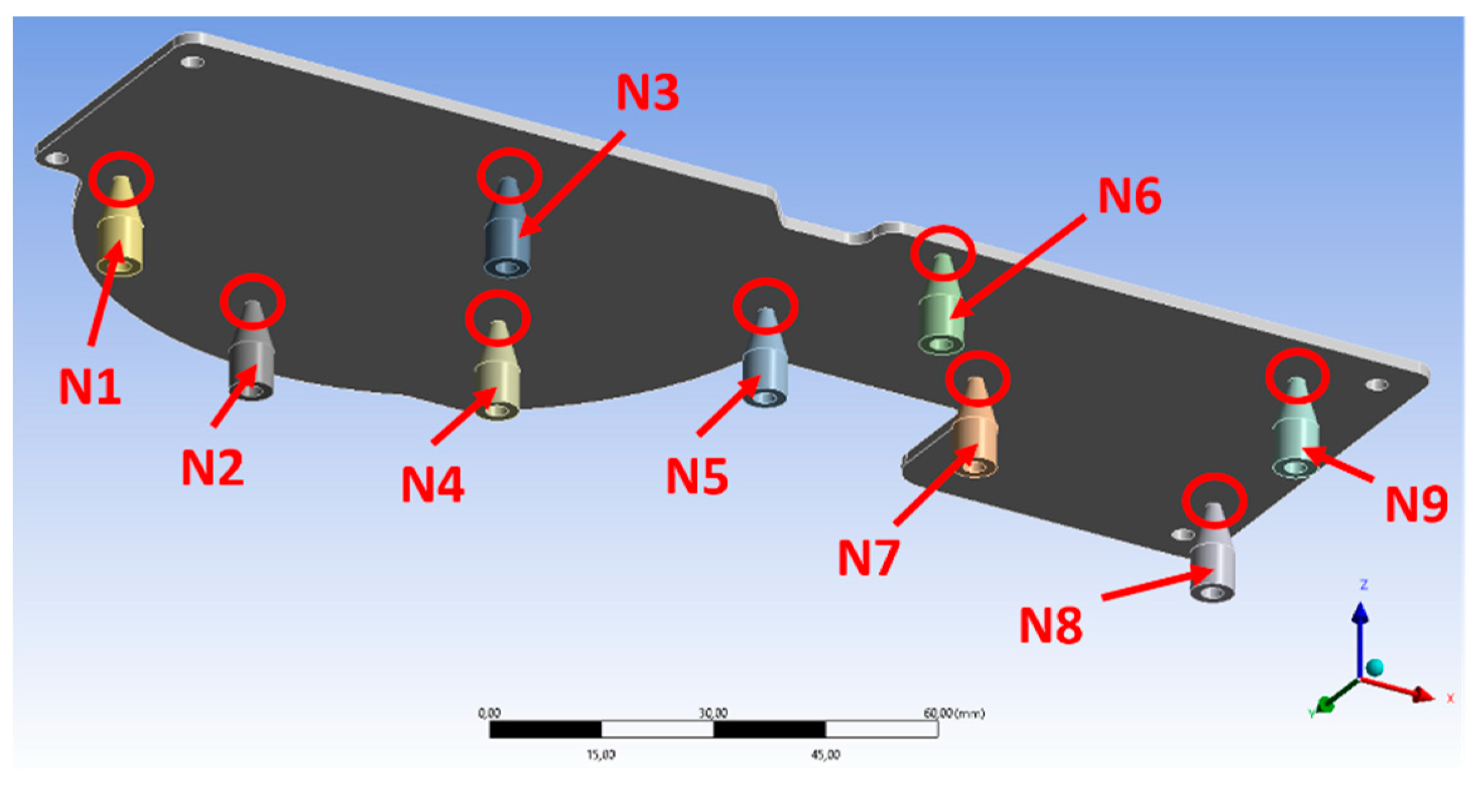
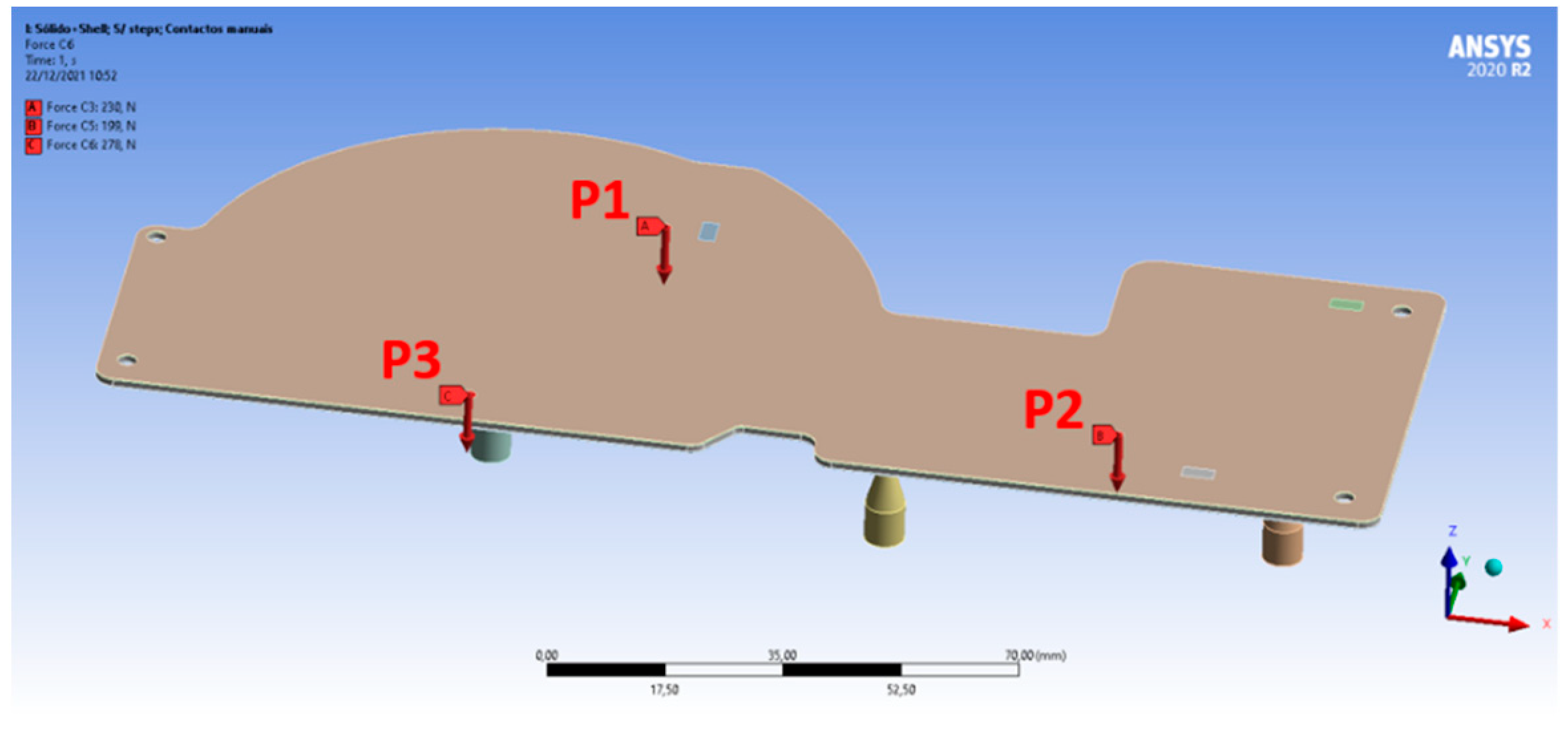
During the experimental tests, the PCB was supported by nine needles and pressed by three pressers. The relative locations of these components are shown in Figure 5 (the letter N identifies the needles and the letter P identifies the pressers).
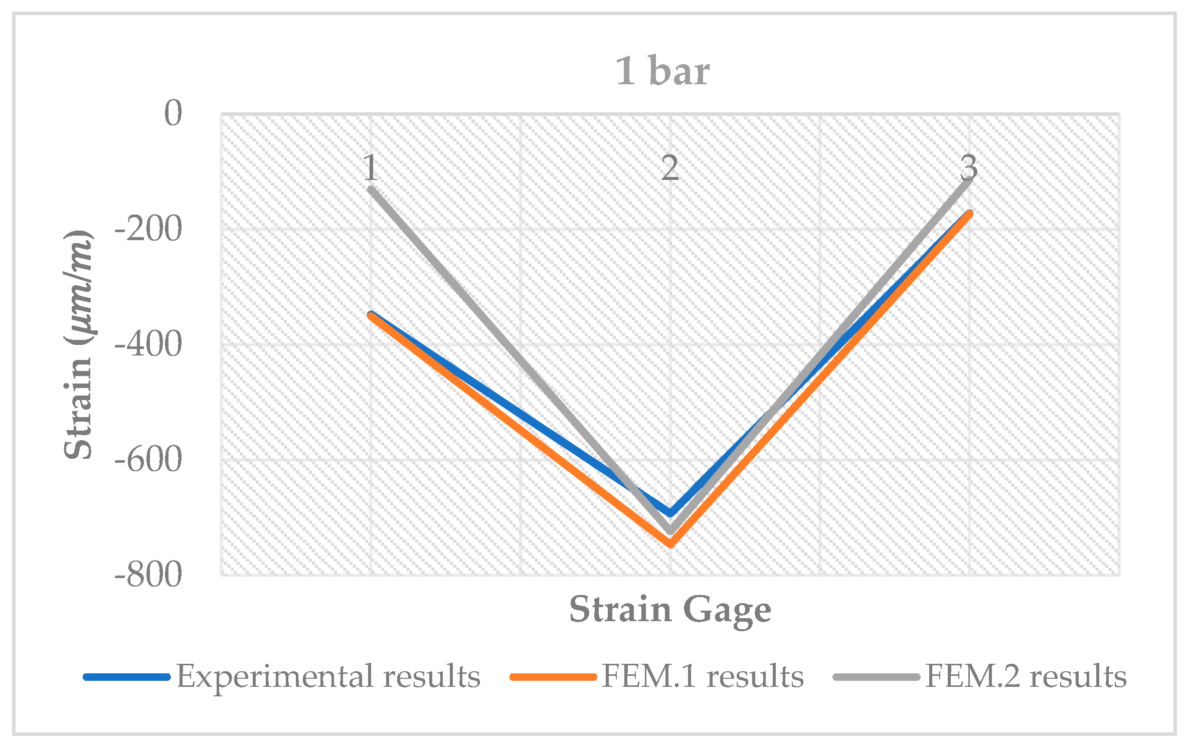
As explained, the force produced by each presser during the experimental tests were measured by load cells. Tests were performed with two different pressures, applied by a pneumatic cylinder: 1 bar and 1.5 bar. Based on the nomenclature in the Figure 5, and arising from each pressure, the forces associated to each of the three pressers are in the Table 1.
These positions were chosen to represent different amounts of copper in the PCB, in different directions. This way, it is possible to obtain different configurations concerning the amount of copper.
Since PCBs have different layers, it is necessary to take into account the amounts of copper on each layer.
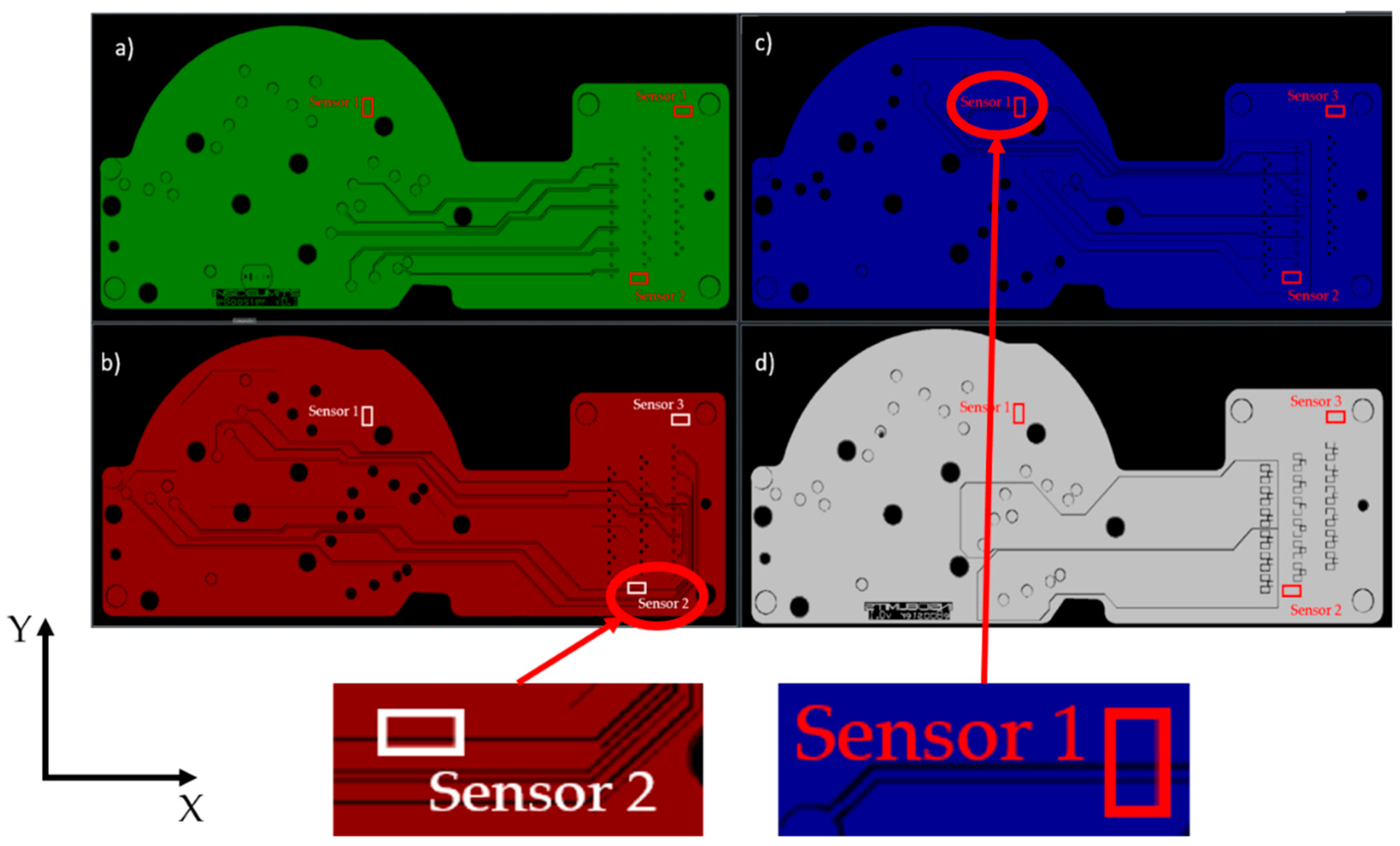
The positions of the three strain gage sensors are presented in Figure 6: (a) 1st copper layer; (b) 2nd copper layer; (c) 3rd copper layer; (d) 4th copper layer.
According to the referential in Figure 6, sensor 1 measures the strain in the Y direction and sensors 2 and 3 measure the strain in the X direction. It is possible to observe that sensor 1 is located above a region of the PCB where there are copper traces perpendicular to the sensor measurement direction in the third layer. Sensor 2 is in a location where it found a copper trace—in the second layer, with the same direction of the sensor measurement direction. Sensor 3 is above a region where there are no copper traces. Thus, it was possible to cover the different basic configurations of copper amounts in a PCB.

2.2. Finite Elements Analysis

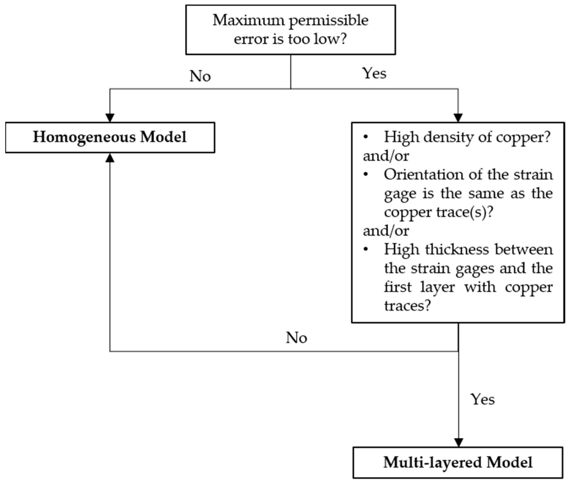
A PCB is a complex device with specific and complex mechanical properties, which vary due to several factors, such as the number of layers, the thickness, the type of fiber of the composite material that attaches the copper traces, the fiber density, and the weavy-style (number of bundles in fill-and-warp directions) [3,19,20]. All these variables need to be taken into account when creating an FEM of a PCB, regardless of the type of study that is being conducted. There are many authors modelling PCBs as a full single material body [2,5,6,7,8,10,12,13,17,18,20,21]; however, to obtain more accurate results, some researchers have opted to create multi-layered models considering the layers of the PCBs [3,11,19,20,22].
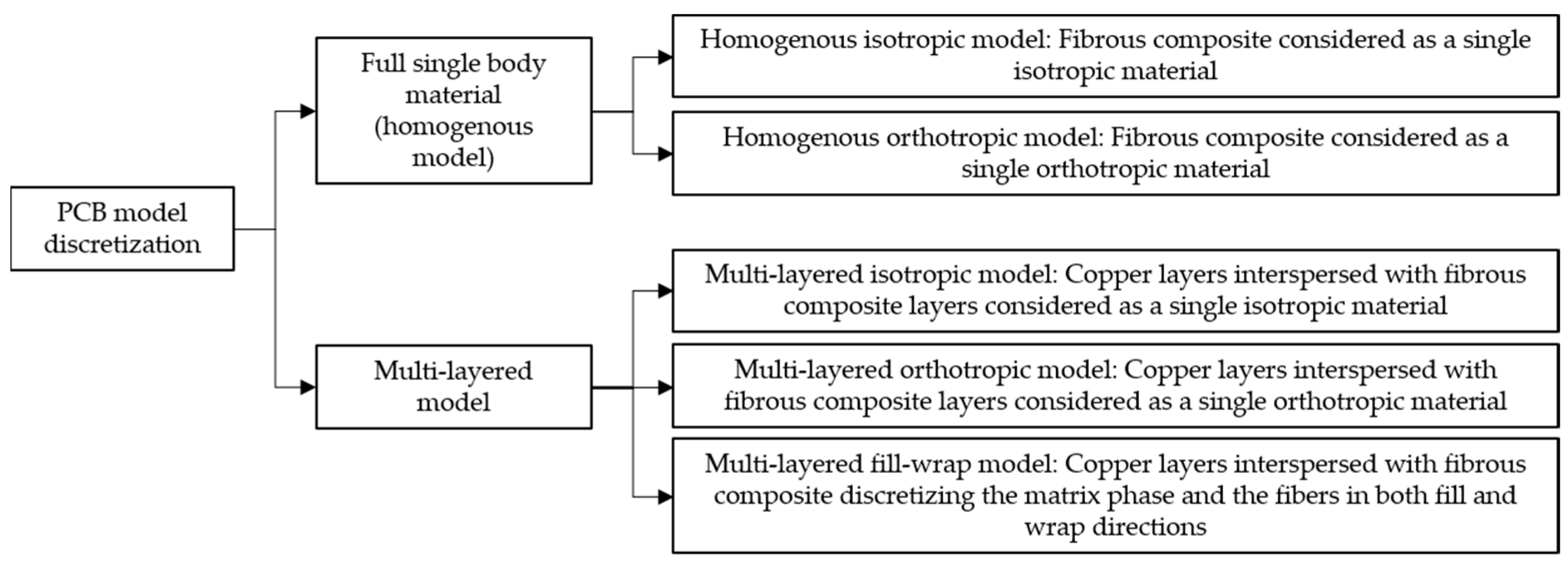
When running PCB numerical simulations, when considering it as a full single material body, it is assumed that the PCBs are a whole body made of a fibrous composite (matrix phase/reinforcement phase plus fiber phase). Under these conditions, the PCB material properties could be considered either isotropic or orthotropic. In full body isotropic models, the PCBs are considered as an elastic–plastic material, defined by a stress–strain curve resultant from tensile tests, and their behaviour follows the von Mises criteria:
G = E 2 ( 1 + v )
where G represents the Shear Modulus, E is the Young Modulus, and v represents the Poisson’s Ratio. In the full body orthotropic model, the fiber phase is neglected and this way, the PCBs are modelled as degenerated bi-phase models, acquiring an orthotropic behaviour [20].
On the other hand, when discretizing the layers of the PCBs, there could be layers made of an electrically conductive material (copper is the most widely used), interspersed with fibrous composite layers. Similarly, fibrous composite layers might be considered either isotropic or as orthotropic. Further, a multi-layered PCB model has been also developed, which divides fibrous composite layers into two sub-layers, with each layer discretizing the fill and wrap fiber directions. The fibers are involved and impregnated in the matrix phase (FR-4 epoxy resin is most widely used for this application) [20].
Figure 7 shows the most common ways to model a PCB.
Y. Wan et al. [20] carried out a study on the mechanical behaviour of a PCB when subjected to a drop impact experimental test. It undoubtedly showed that the multi-layered fill-wrap model allows for the most accurate and realistic FE analysis. However, the computational requirements and the time required to run the simulations are extremely high. It also stated, as expected, that the isotropic model is the worst representation of reality if the results collected from the drop-impact experimental test are the most disparate.
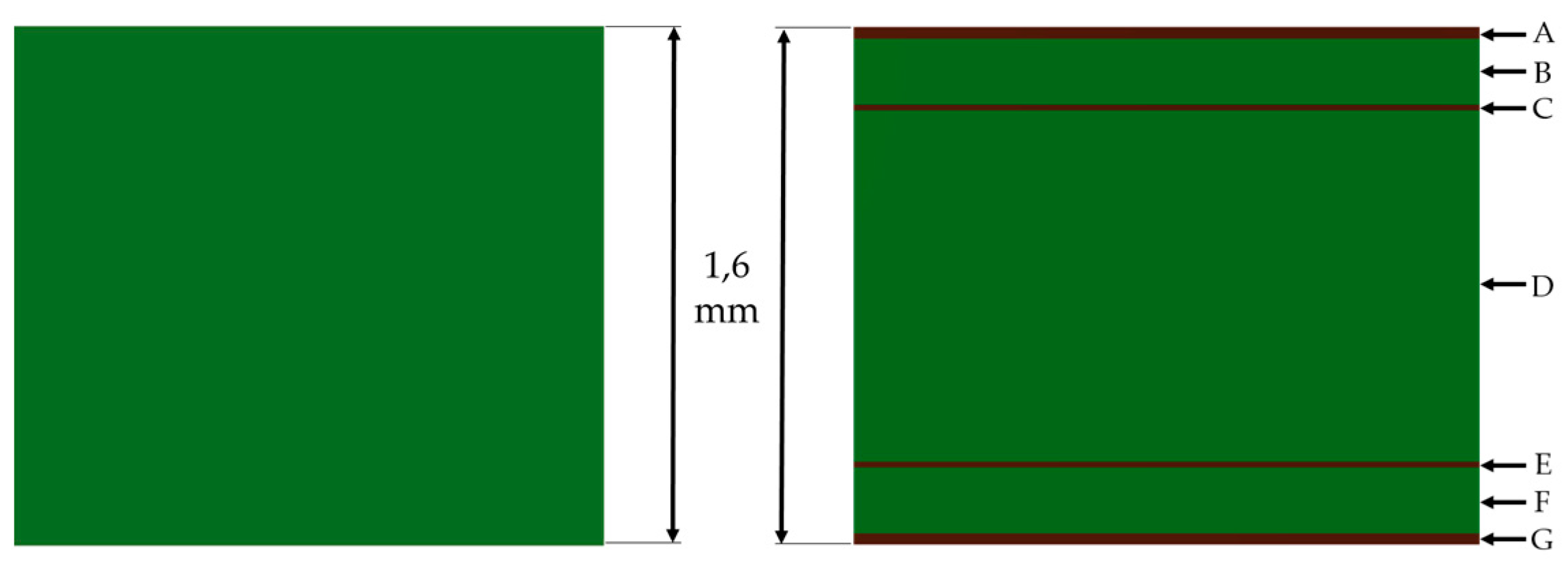
The present work tried to find out the best FEM to simulate PCB behaviour during ICTs. It used a 1.6 mm thick, multi-layered PCB (four copper layers) named eBooster.
Figure 8 shows the schematic sectional view of eBooster when considering both homogeneous and multi-layered models.
Layer thickness and materials of multi-layer PCBs models are presented in Table 2.
Once the PCB was made using an orthotropic fibrous composite reinforcement (woven E-glass FR-4 epoxy resin), the following two FEM were created:
  • FEM.1: Homogenous orthotropic model with solid element meshing
  • FEM.2: Multi-layered orthotropic model with solid element meshing representing the fibrous composite layers and with shell element meshing representing the copper layers
The mechanical properties of each material of the PCB are tabulated in Table 3.
In order to match the simulation approach with the experimental setup—as described in Section 2.2—the software Ansys was used. Apart from FEM, the boundary conditions that rule all the FEA were the same. The PCB was supported by needles and loaded by pressers, and the material assigned to the needles was structural steel in order to represent the reality created in the experimental setup. The contacts between the needles and the PCB were defined as rough with the formulation adjust to touch. This type of contact allows gaps or penetration between the contact and target surfaces, once the FEM surfaces are mathematically approximated. In Figure 9, the needles and their contacts with the PCB are shown. In Figure 10, the locations where the three pressers load the PCB are represented. Naturally, those locations were based on the pressers’ locations in the experimental tests.
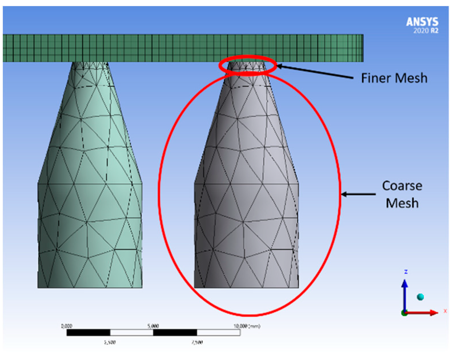
Fine mesh face sizings were applied to the needles’ faces that were in contact with the PCB. Once these contacts were defined as rough with the formulation adjust to touch, this face sizing is a crucial step, since it will prevent excessive penetration between the needles’ elements and the PCB elements.
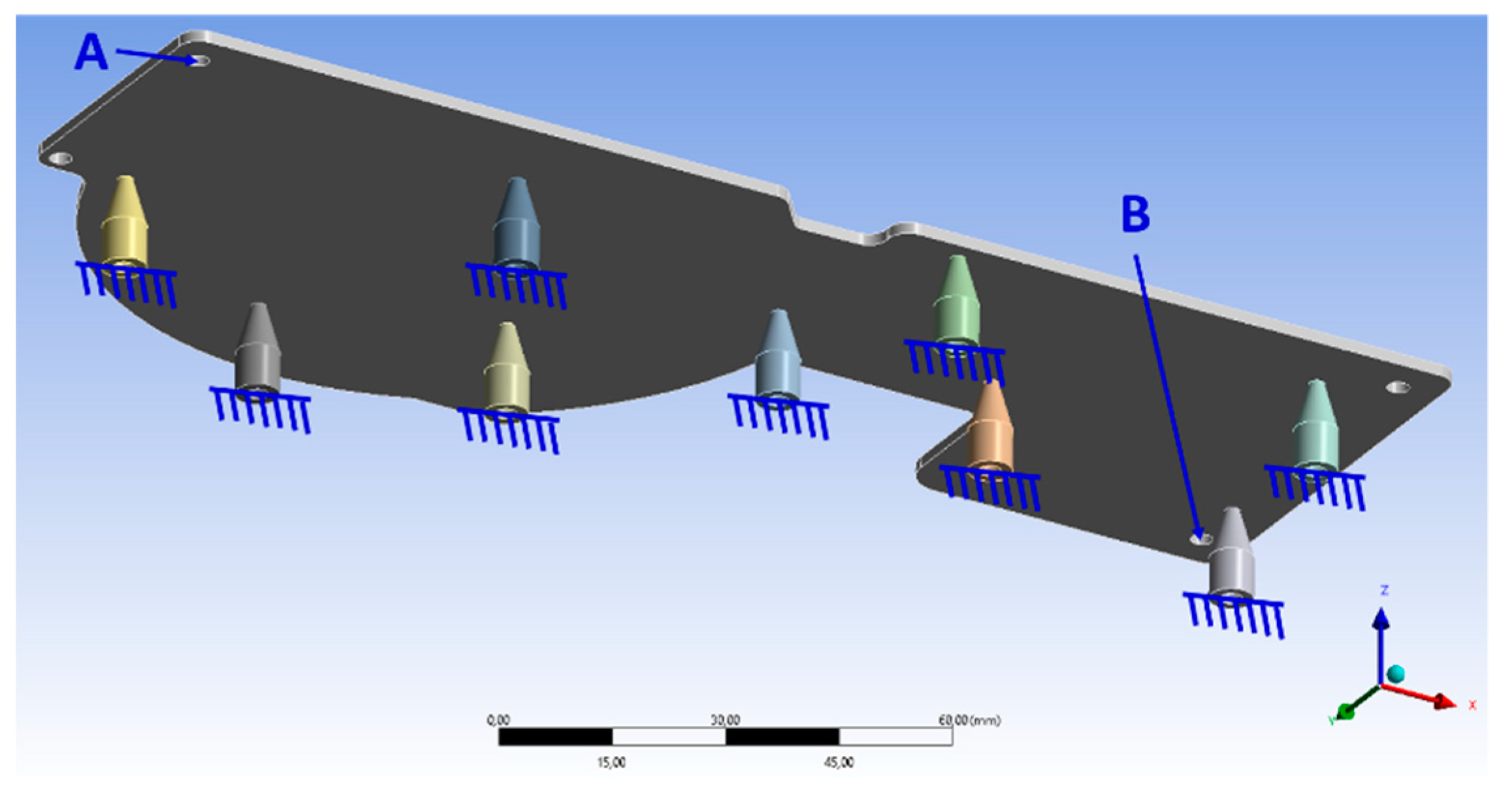
The interior walls of the guiding holes (denoted as A and B in Figure 11), where the fixing pins are inserted to fix the PCB, were constrained as fixed. This means the holes are prevented from any kind of motion. Further, the needles were considered as grounded in order to restrain their movement in the Z-axis (Figure 11).
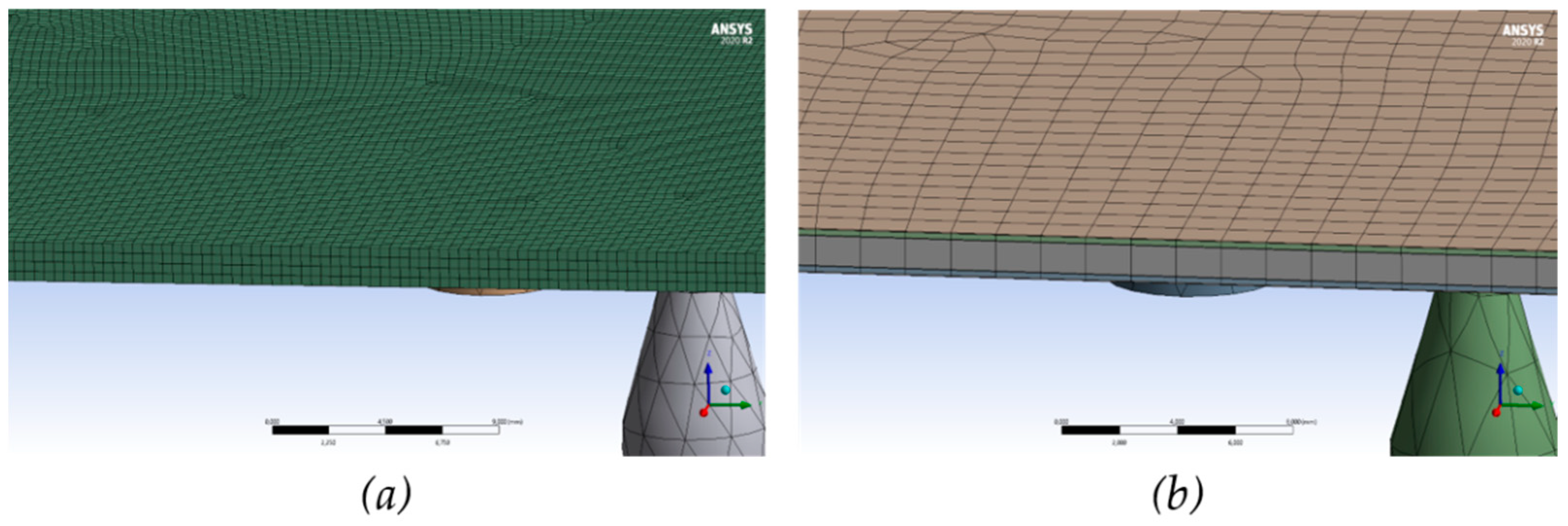
In FEM.1, a multizone method was applied to the PCB, and it was defined with hexahedral elements which fit within the PCB geometry, allowing to obtain excellent mesh metrics properties. Once the needles are out of the interest region, they are meshed with a default coarse mesh (automatic method) to reduce computational analysis complexity. However, fine mesh face sizing was applied to the needles’ faces that were in contact with the PCB (Figure 12). In FEM.2, the copper layers were meshed with shell elements and the fibrous composite layers were meshed with solid elements. To fit within the thinner copper layers, the quadrilateral method was used. A multizone method with hexahedral elements was used on the solid elements layers. Part of the meshes of both FEM can be seen in Figure 13.
In order to match the experimental setup, the three strain gages were modelled in corresponding locations and orientations as rectangular prisms, with negligible thickness, and meshed with a single shell element (Figure 14).
Since each strain gage is a single element, during the pre-processing phase, it was ordered to the Ansys to return the element mean strain for each of the three created strain gages. The measurement orientation of each strain gage was selected in accordance with the experimental test setup.
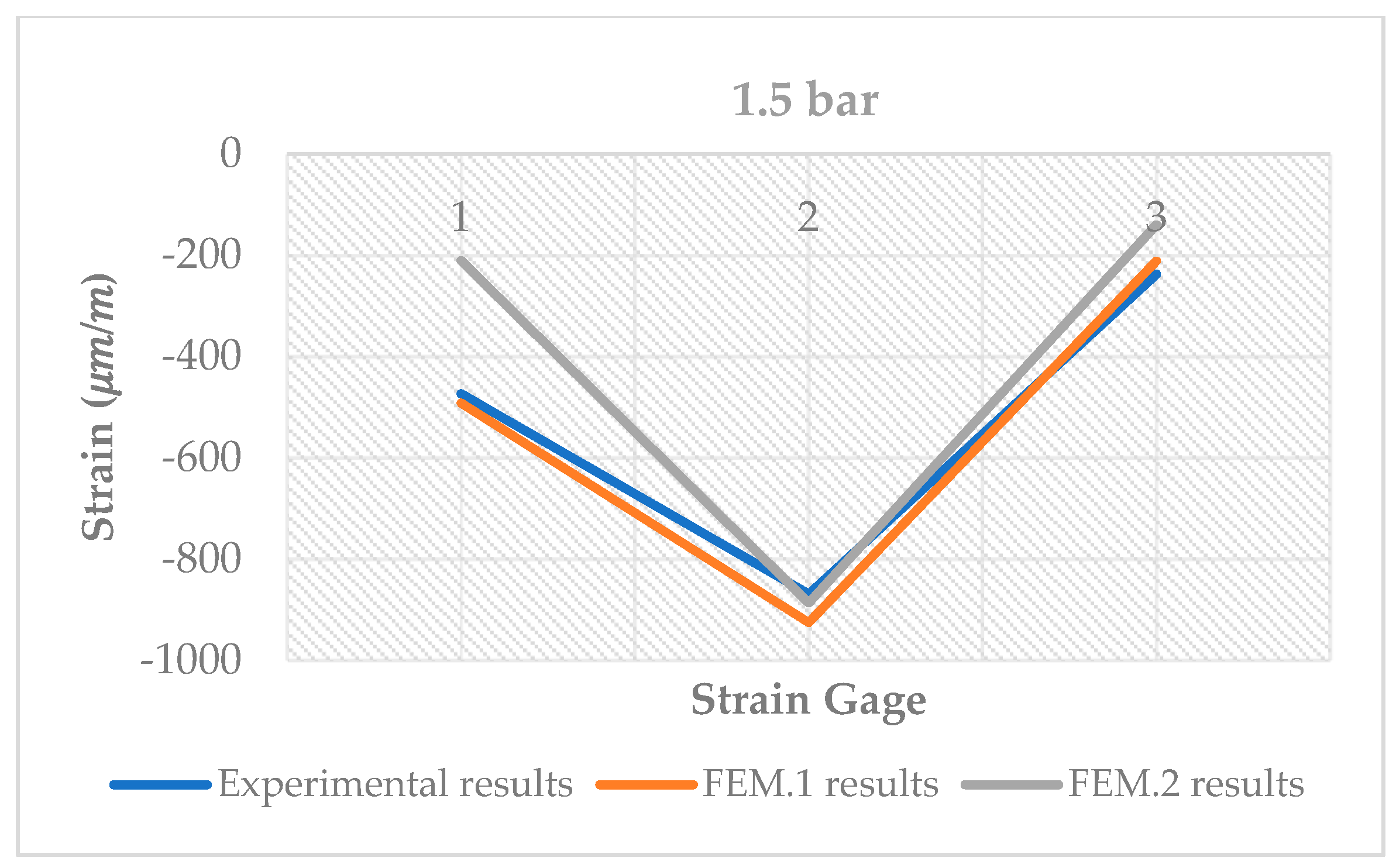
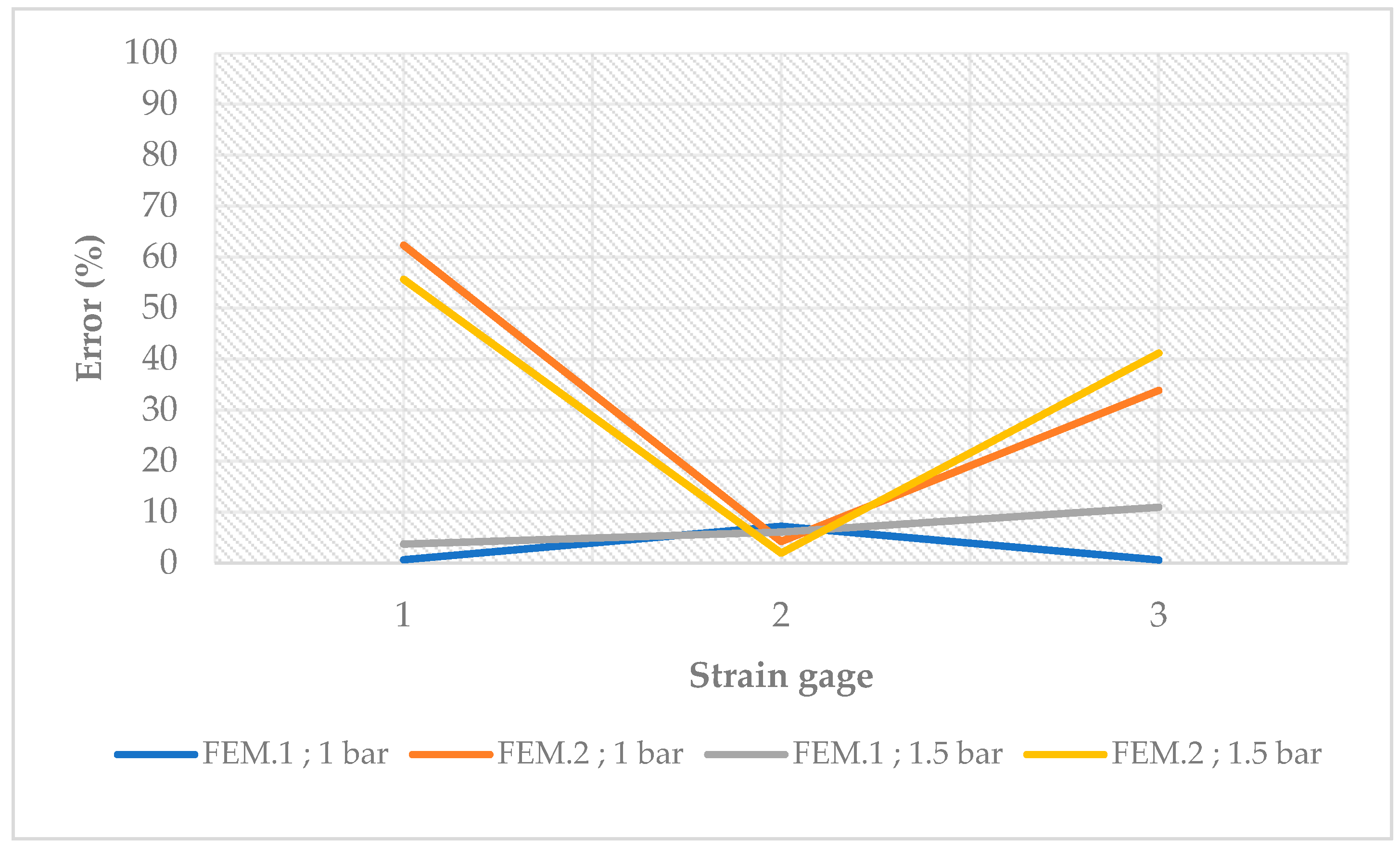
Thus, Finite Element Analysis for each of the two FEM was performed, applying forces performed by the three pressers. The forces measured during the experimental tests were followed, namely, those that resulted from the pneumatic pressures of 1 bar and 1.5 bar.

3. Results

The results from the experimental test and Finite Element analyses are exposed in this chapter in order to provide an overview of the accuracy of the results themselves. The experimental results and the results from the Finite Element Analysis of the two FEM are presented.

3.1. Experimental Results

As stated in Section 2.1, a PCB was experimentally tested in bending efforts and strains were measured in three distinct areas by mean of three different strain gages. In addition, as referred to in Section 2.1, a set of experimental tests were conducted that allowed to acquire strain data, graphically and numerically.
For instance, the graphics obtained from one of the experimental tests (1 bar) are shown in Figure 15. The green, red, and blue lines correspond to the data recorded by strain gages 1, 2, and 3, respectively.
Table 4 presents the strains measured (averaged) by the three strain gages, from all the experimental tests, for both 1 and 1.5 bar.

3.2. Finite Element Analysis

As per the process described in Section 2.2, FEA of both FEM.1 and FEM.2 were performed.
Table 5 and Table 6 present the obtained strains by each of the three strain gages, for both 1 and 1.5 bar pressures, when running simulations with FEM.1 and FEM.2, respectively.
The time required for the numerical simulation of the FEM.1 and FEM.2 models are stated in Table 7. It is important to note that the PC used was an HP OMEN Serie 15-en0000 with 16 Gb RAM and an AMD Ryzen 7 4800H processor. In addition, Table 7 shows the number of nodes and elements of each of the meshes of FEM.1 and FEM.2. The required time refers to the FEA, considering a pressure of 1.5 bar.
The numerical analysis with FEM.2 took more time than FEM.1, despite the higher number of nodes and elements in the latter. This is due to the higher complexity of FEM.2, as this model, being multi-layered, entails more contact definition, namely, between layers.
Figure 16 allows to graphically compare the experimental results with the FEA results when the PCB is subjected to resultant forces from 1 bar of pressure. Figure 17 provides the results when 1.5 bar of pressure is used.
It is possible to conclude that, regardless of the pressure, when compared to the experimental results, the FEM.1 model provides accurate results for all the three strain gages. The FEM.2 presents a more accurate strain value regarding strain gage 2. For a better insight into these strain values, the errors between the experimental and FEA results (based on the experimental results) were calculated, disclosed in Table 8 and Figure 18.
It is clear that the strain values of strain gage 2, regardless of the adopted pressure as well as the FEM, is the most accurate strain gage and with the most stable values. In addition, it can be observed that the error associated with the measurements of strain gages 1 and 3 increases exponentially when using a pressure of 1.5 bar. Ever so slightly, it is the other way around with the error associated with strain gage 2.

4. Discussion

Even when not considering the PCB as a multi-layer body in model FEM.1, the strain values, resulting from the numerical simulations, seem to be really accurate. This stems from the PCB’s low copper density. The FEM.1 model, which is not modeled with copper layers, represents reality well. This is the conclusion when observing the strain values from the experimental setup, side-by-side with the results obtained from the numerical simulations using FEM.1. These values are displayed in the following two tables (Table 9 and Table 10) considering the tests using 1 bar and 1.5 bar, respectively.
It is observed that at pressure of 1.5 bar, the error tends to increase, as was expected.
Table 11 and Table 12 provide a comparison between the experimental and numerical analysis results for the FEM.2 model.
Unlike the FEM.1 model, it was observed that, when using FEM.2, there is no universal behavior of strain values increment when the applied force is increased. It is possible to conclude that the error associated with strain gages 1 and 2 decreases with the force increment and, conversely, with strain gage 3, the error value increases. As shown in Section 2.1., strain gages 1 and 2 are in zones above copper traces. It accomplishes the expected: models having copper layers provide better strain results in zones where PCBs have copper traces, when compared to homogeneous models. However, it is observable that only the strain values obtained by FEA for strain gage 2 are notably close to the strain values measured in the experimental tests (errors of 4.23% and 1.95% in Table 11 and Table 12, respectively).
The strain values obtained from numerical simulation of the FEM.2 model, with strain gage 1, are not close to the values experimentally obtained with strain gage 2. This might be because strain gage 1 was above a copper trace only in the third copper layer, as described in Section 2.1 (Figure 6). In other words, in the real PCB, there was a thickness of 1.3175 mm separating strain gage 1 from the copper trace (Table 2), unlike what is verified in the FEM.2 model, where the two superior copper layers of the PCB are represented. In addition to the thickness between the strain gages and the first layer with copper traces, the copper traces’ orientation might also be a factor to consider because, in contrast to what is verified in strain gage 1, strain gage 2 shares the same orientation as the copper trace underneath it and presents better results.
When comparing the results of the two models—FEM.1 and FEM.2—to the experimental results, it is undoubtedly seen that FEM.1 has a higher level of accuracy with regard to strain gages 1 and 3. On the other hand, FEM.2 generates slightly more accurate results for strain gage 2 if, in the real PCB, the thickness separating the strain gage from the second layer is small (0.235 mm; Table 2).

5. Conclusions

A homogeneous model of a PCB is a good approach to reality, provided that the maximum permissible error is very low. It might be necessary to use a multi-layer model, depending on the morphology of the PCB under study.
It is also concluded that regarding PCBs, or PCBs zones, with a low copper trace density, homogenous numeric models realistically simulate the PCBs. In zones where there are copper traces in the same orientation as the strain gages, multi-layers models allow to obtain results that are more accurate. Further, in zones where the copper traces are not too “deep” in the PCB, these same copper traces affect the numerical results. Therefore, in these cases, multi-layers numeric models should be used.
Based on this information, the following methodology was built for systematic analysis of PCB bending simulations during ICTs (Figure 19).
However, to consolidate this methodology and for future research, a wider variety of PCBs should be tested in order to define how the FEA of a multi-layered FEM behaves.
It is also necessary to test more PCBs with different copper amounts to create value ranges of copper trace density, which define low or high copper density. With this, the team expects to move from the qualitative approach presented here to a quantitative approach. In addition, it is necessary to confirm the influence of copper trace orientation and thickness separating the copper traces and the strain gages.

Author Contributions

Conceptualization, R.O. and L.F.; methodology, R.O. and L.F.; software, R.O. and D.C.; validation, R.O., L.F. and D.C.; formal analysis, A.M.G., T.M. and J.M.; investigation, R.O. and L.F.; resources, J.V. and J.M.; data curation, R.O.; writing—original draft preparation, R.O.; writing—review and editing, L.F., J.M., A.M.G. and T.M.; visualization, R.O. and L.F.; supervision, J.M. and J.V.; project administration, J.M. and J.V.; funding acquisition, J.M. and J.V. All authors have read and agreed to the published version of the manuscript.

Funding

This work is co-funded by the European Regional Development Fund (ERDF) through the North Regional Operational Program (NORTE 2020) of the Portugal 2020 Program (Project No. 43922, with acronym “iFixturing”; Funding Reference NORTE-01-0247-FEDER-043922).

Informed Consent Statement

Not applicable.

Acknowledgments

The authors thank Portuguese North Regional Operational Program (NORTE 2020), InsideLimits company, and MEtRICs Research Center for all support provided.

Conflicts of Interest

The authors declare no conflict of interest. The funders had no role in the design of the study; in the collection, analyses, or interpretation of data; in the writing of the manuscript, or in the decision to publish the results.

References

  1. Freitas, L.; Oliveira, R.; Malheiro, T.; Gonçalves, A.M.; Vicente, J.; Monteiro, P.; Ribeiro, P. Conceptual Design of a Positioning System for Systematic Production of Needle Beds. In Lecture Notes in Mechanical Engineering, Proceedings of the Innovations in Mechatronics Engineering; Machado, J., Soares, F., Trojanowska, J., Yildirim, S., Eds.; Springer International Publishing: Cham, Switzerland, 2022; pp. 221–235. [Google Scholar]
  2. Marsavina, L.; Falk, A.; Pop, O. Analysis of Printed Circuit Boards Strains Using Finite Element Analysis and Digital Image Correlation. Frat. Integrità Strutt. 2019, 14, 541–551. [Google Scholar] [CrossRef]
  3. Li, L.; Kim, S.M.; Song, S.H.; Ku, T.W.; Song, W.J.; Kim, J.; Chong, M.K.; Park, J.W.; Kang, B.S. Finite Element Modeling and Simulation for Bending Analysis of Multi-Layer Printed Circuit Boards Using Woven Fiber Composite. J. Mater. Process. Technol. 2008, 201, 746–750. [Google Scholar] [CrossRef]
  4. Ma, H.; Liu, K.-C.; Lee, T.-K.; Kim, D.H. Effects of PCB Design Variations on Bend and ATC Performance of Lead-Free Solder Joints. In Proceedings of the 2010 Proceedings 60th Electronic Components and Technology Conference (ECTC), Las Vegas, NV, USA, 1–4 June 2010; IEEE: Las Vegas, NV, USA, 2010; pp. 1512–1517. [Google Scholar]
  5. Wang, J.; He, P.; Xiao, F. The Effect of Residual Stress on the Flexing Strength of PCB Assembly. In Proceedings of the Proceedings of the Sixth IEEE CPMT Conference on High Density Microsystem Design and Packaging and Component Failure Analysis (HDP ’04), Shanghai, China, 3 July 2004; IEEE: Shanghai, China, 2004; pp. 146–150. [Google Scholar]
  6. Harada, K.; Baba, S.; Wu, Q.; Matsushima, H.; Matsunaga, T.; Ucgai, Y.; Kimura, M. Analysis of Solder Joint Fracture under Mechanical Bending Test. In Proceedings of the 53rd Electronic Components and Technology Conference, New Orleans, LA, USA, 27–30 May 2003; IEEE: New Orleans, LA, USA, 2003; pp. 1731–1737. [Google Scholar]
  7. Chengalva, M.K.; Jeter, N.; Baxter, S.C. Effect of Circuit Board Flexure on Flip Chips before Underfill. In Proceedings of the 2000 Proceedings. 50th Electronic Components and Technology Conference (Cat. No.00CH37070), Las Vegas, NV, USA, 21–24 May 2000; IEEE: Las Vegas, NV, USA, 2000; pp. 657–665. [Google Scholar]
  8. Geng, P.; Chen, P.; Ling, Y. Effect of Strain Rate on Solder Joint Failure under Mechanical Load. In Proceedings of the 52nd Electronic Components and Technology Conference 2002. (Cat. No.02CH37345), San Diego, CA, USA, 28–31 May 2002; IEEE: San Diego, CA, USA, 2002; pp. 974–978. [Google Scholar]
  9. Patwardhan, V.; Chin, D.; Wong, S.; Rey, E.; Kelkar, N.; Nguyen, L. Flexural Testing of Board Mounted Wafer Level Packages for Handheld Devices. In Proceedings of the Proceedings Electronic Components and Technology, 2005. ECTC ’05, Lake Buena Vista, FL, USA, 31 May–3 June 2005; IEEE: Lake Buena Vista, FL, USA, 2005; Volume 2, pp. 557–561. [Google Scholar]
  10. Hsieh, G.; Mcallister, A. Flip Chip Ball Grid Array Component Testing under Board Flexure. In Proceedings of the Proceedings Electronic Components and Technology, 2005. ECTC ’05, Lake Buena Vista, FL, USA, 31 May–3 June 2005; IEEE: Lake Buena Vista, FL, USA, 2005; Volume 2, pp. 937–944. [Google Scholar]
  11. Seah, S.K.W.; Lim, C.T.; Tan, V.B.C.; Quah, S.E. Study of Microvia Failure under PCB Flexing Loads. In Proceedings of the 53rd Electronic Components and Technology Conference, New Orleans, LA, USA, 27–30 May 2003; IEEE: New Orleans, LA, USA, 2003; pp. 95–99. [Google Scholar]
  12. Jie, G.; Lim, C.T.; Tay, A.A.O. Modeling of Solder Joint Failure Due to PCB Bending during Drop Impact. In Proceedings of the Proceedings of 6th Electronics Packaging Technology Conference (EPTC 2004) (IEEE Cat. No.04EX971), Singapore, 8–10 December 2004; IEEE: Singapore, 2004; pp. 678–683. [Google Scholar]
  13. Wang, S.; Chen, Y.; Zheng, L.; Chen, Y.; Zhang, H.; Gong, L.; Chen, B.; He, W. Dropping Simulation of Printed Circuit Board with BGA Soldering Assembly for Optical Module Application. In Proceedings of the 2016 International Conference on Modeling, Simulation and Optimization Technologies and Applications (MSOTA2016), Xiamen, China, 18–19 December 2016; Atlantis Press: Xiamen, China. [Google Scholar]
  14. Yamaji, Y.; Suzuki, T.; Yamasaki, H.; Ohishi, T.; Chikawa, Y.; Kako, N. New Evaluation Method of CSPs Board Level Reliability Using Strain Gauge. In Proceedings of the 2000 Proceedings. 50th Electronic Components and Technology Conference (Cat. No.00CH37070), Las Vegas, NV, USA, 21–24 May 2000; IEEE: Las Vegas, NV, USA, 2000; pp. 1398–1404. [Google Scholar]
  15. Arzhanov, B.; Correia, A.; Delgado, P.; Meireles, J. Thermal Evaluation of Printed Circuit Board Design Options and Voids in Solder Interface by a Simulation Tool. Int. J. Mech. Mechatron. Eng. 2016, 10, 494–505. [Google Scholar]
  16. Arzhanov, B.; Correia, A.; Delgado, P.; Meireles, J. Monitorization of Junction Temperature Using a Thermal-Test-Device. Int. J. Mech. Mechatron. Eng. 2016, 10, 521–531. [Google Scholar]
  17. Long, L.; Li, G.; Liao, X.; Xie, B.; Shi, X. Dynamic Bending Test and Simulation of PBGA Packages. In Proceedings of the 2011 12th International Conference on Electronic Packaging Technology and High Density Packaging, Shanghai, China, 8–11 August 2011; IEEE: Shanghai, China, 2011; pp. 1–5. [Google Scholar]
  18. Yu, D.; Kwak, J.B.; Park, S.; Lee, J. Dynamic Responses of PCB under Product-Level Free Drop Impact. Microelectron. Reliab. 2010, 50, 1028–1038. [Google Scholar] [CrossRef]
  19. Liu, K.; Lu, C.; Tai, N.-H.; Yeh, M.-K. Stress Analysis of Printed Circuit Board with Different Thickness and Composite Materials Under Shock Loading. Comput. Model. Eng. Sci. 2020, 122, 661–674. [Google Scholar] [CrossRef]
  20. Wang, Y.; Low, K.H.; Pang, H.L.J.; Hoon, K.H.; Che, F.X.; Yong, Y.S. Modeling and Simulation for a Drop-Impact Analysis of Multi-Layered Printed Circuit Boards. Microelectron. Reliab. 2006, 46, 558–573. [Google Scholar] [CrossRef]
  21. Fan, X.; Pei, M.; Bhatti, P.K. Effect of Finite Element Modeling Techniques on Solder Joint Fatigue Life Prediction of Flip-Chip BGA Packages. In Proceedings of the 56th Electronic Components and Technology Conference 2006, San Diego, CA, USA, 30 May–2 June 2006; IEEE: San Diego, CA, USA, 2006; pp. 972–980. [Google Scholar]
  22. Kim, D.-H.; Joo, S.-J.; Kwak, D.-O.; Kim, H.-S. Warpage Simulation of a Multilayer Printed Circuit Board and Microelectronic Package Using the Anisotropic Viscoelastic Shell Modeling Technique That Considers the Initial Warpage. IEEE Trans. Compon. Packag. Manuf. Technol. 2016, 6, 1667–1676. [Google Scholar] [CrossRef]
Figure 1. Adapted Machine for the Experimental Setup.
Machines 10 00135 g001
Figure 2. Support and guiding pins.
Machines 10 00135 g002
Figure 3. Pressers.
Figure 3. Pressers.
Machines 10 00135 g003
Figure 4. PCB under study with the three strain gages attached.
Machines 10 00135 g004
Figure 5. Relative locations of the needles and pressers.
Machines 10 00135 g005
Figure 6. Strain gage sensors’ positions in relation to PCB layers: (a) 1st layer; (b) 2nd layer; (c) 3rd layer; (d) 4th layer.
Machines 10 00135 g006
Figure 7. Five usual ways of modelling PCBs.
Machines 10 00135 g007
Figure 8. Schematic sectional view of the PCB eBooster: (a) Homogeneous model; (b) multi-layer model.
Machines 10 00135 g008
Figure 9. Needles’ notation and their contact zones with PCBs.
Machines 10 00135 g009
Figure 10. Pressers’ load locations.
Machines 10 00135 g010
Figure 11. Illustration of the grounded needles and the fixed guiding holes.
Machines 10 00135 g011
Figure 12. Needles’ mesh zones.
Machines 10 00135 g012
Figure 13. Illustration of the mesh of both analysed FEM: (a) FEM.1; (b) FEM.2.
Machines 10 00135 g013
Figure 14. Strain gages modelation.
Machines 10 00135 g014
Figure 15. Data acquired by three strain gages during one of the experimental test (1 bar).
Machines 10 00135 g015
Figure 16. Experimental results vs FEA results (1 bar).
Machines 10 00135 g016
Figure 17. Experimental results vs FEA results (1.5 bar).
Machines 10 00135 g017
Figure 18. Percentual error of the FEA results, compared to the experimental results.
Machines 10 00135 g018
Figure 19. Methodology for systematic analysis of PCB bending simulation during ICTs.
Machines 10 00135 g019
Table 1. Force applied by each presser during the experimental tests.
PressurePresser P1Presser P2Presser P3
1 bar163 N162 N184 N
1.5 bar230 N199 N278 N
Table 2. Layer Thickness and Materials.
LayersPCB eBooster
Thickness (mm)Material
A0.0350Copper
B0.2000Fibrous composite
C0.0175Copper
D1.0650Fibrous Composite
E0.0175Copper
F0.2000Fibrous Composite
G0.0350Copper
Table 3. Mechanical properties of fibrous composite reinforcement and copper.
PropertiesFibrous Composite
(Woven E-Glass FR-4 Epoxy Resin)
Copper
Young Modulus (MPa) E x 24.000110.000
E y 23.000
E z 15.000
Shear Modulus (MPa) G x y 9.200
G y z 8.40040.953
G x z 6.600
Poisson’s Ratio v x y 0.11
v y z 0.090.343
v x z 0.14
Table 4. Experimental strains measured.
1 bar1.5 bar
Strain gage 1−348 µm/m−473 µm/m
Strain gage 2−693 µm/m−869 µm/m
Strain gage 3−172 µm/m−237 µm/m
Table 5. Strain results from FEA of FEM.1.
1 bar1.5 bar
Strain gage 1−350.35 µm/m−491.21 µm/m
Strain gage 2−746.72 µm/m−925.15 µm/m
Strain gage 3−173.01 µm/m−211.05 µm/m
Table 6. Strain results from FEA of FEM.2.
1 bar1.5 bar
Strain gage 1−131.16 µm/m−209.83 µm/m
Strain gage 2−723.58 µm/m−886.25 µm/m
Strain gage 3−113.75 µm/m−139.45 µm/m
Table 7. Required time and number of nodes and elements.
TimeNodesElements
FEM.132 min1.544.313327.644
FEM.21 h 55 min456.860127.728
Table 8. Percentual error of the FEA results, compared to the experimental results.
1 bar1.5 bar
FEM.1FEM.2FEM.1FEM.2
Strain gage 10.67%62.31%3.71%55.64%
Strain gage 27.19%4.23%6.07%1.95%
Strain gage 30.58%33.87%10.95%41.16%
Table 9. Comparison of strain values in the experimental and numerical analyses of the FEM.1 model (1 bar).
1 bar
Experimental ResultsFEM.1Error
Strain gage 1−348 µm/m−350.35 µm/m0.67%
Strain gage 2−693 µm/m−746.72 µm/m7.19%
Strain gage 3−172 µm/m−173.01 µm/m0.58%
Table 10. Comparison of strain values in the experimental and numerical analyses of the FEM.1 model (1. 5 bar).
1.5 bar
Experimental ResultsFEM.1Error
Strain gage 1−473 µm/m−491.21 µm/m3.71%
Strain gage 2−869 µm/m−925.15 µm/m6.07%
Strain gage 3−237 µm/m−211.05 µm/m10.95%
Table 11. Comparison of strain values in the experimental and numerical analyses for the FEM.2 model (1 bar).
1 bar
Experimental ResultsFEM.2Error
Strain gage 1−348 µm/m−131.16 µm/m62.31%
Strain gage 2−693 µm/m−723.58 µm/m4.23%
Strain gage 3−172 µm/m−113.75 µm/m33.87%
Table 12. Comparison of strain values in the experimental and numerical analyses for the FEM.2 model (1.5 bar).
1.5 bar
Experimental ResultsFEM.2Error
Strain gage 1−348 µm/m−209.83 µm/m55.64%
Strain gage 2−693 µm/m−886.25 µm/m1.95%
Strain gage 3−172 µm/m−139.45 µm/m41.16%
Publisher’s Note: MDPI stays neutral with regard to jurisdictional claims in published maps and institutional affiliations.

