Article

Reliable Design and Control Implementation of Parallel DC/DC Converter for High Power Charging System

Unmanned System Research Institute, Northwestern Polytechnical University, Xi’an 710072, China
*
Author to whom correspondence should be addressed.
Machines 2022, 10(12), 1162; https://doi.org/10.3390/machines10121162
Submission received: 2 November 2022 / Revised: 27 November 2022 / Accepted: 30 November 2022 / Published: 4 December 2022
(This article belongs to the Topic Energy Equipment and Condition Monitoring)

Abstract

:
With the current popularity of Electric Vehicles (EV), especially in some critical EV applications such as hospital EV fleets, the demand for continuous and reliable power supply is increasing. However, most of the charging stations are powered in a centralized way, which causes transistors and other components to be subjected to high voltage and current stresses that reduce reliability, and a single point of failure can cause the entire system to fail. Therefore, a significant effort is made in this paper to improve the reliability of the charging system. In terms of charging system structure design, a distributed charging structure with fault tolerance is designed and a mathematical model to evaluate the reliability of the structure is proposed. In terms of control, a current sharing control algorithm is designed that can achieve fault tolerance. To further improve the reliability of the system, a thermal sharing control method based on current sharing technology is also designed. This method can improve the reliability of the charging system by distributing the load more rationally according to the differences in component performance and operating environment; FPGA-based control techniques are provided, and innovative ideas of pipeline control and details of mathematical reasoning for key IP cores are presented. Experiments show that N + 1 redundancy fault tolerance can be achieved in both current sharing and thermal sharing modes. In the current sharing experiment, when module 3 failed, the total current only fluctuated 800 mA within 500 ms, which is satisfactory. In the thermal sharing experiment, after module 3 failed, modules 1, 2, and 4 adjusted the current reasonably under the correction of the thermal sharing loop, and the total current remained stable throughout the process. The experimental results prove that the charging system structure design and control method proposed in this paper are feasible and excellent.

1. Introduction

Currently, EV adoption is expanding at a rapid pace. The International Energy Agency (IEA) estimates that by 2030, the global four-wheeled electric vehicle fleet will reach approximately 140 million, while electric vehicle sales will reach 25 million units per year [1]. High power switching power supplies are commonly used in charging stations. The continuous and reliable power supply of the charging system can be of great importance to ensure the safe and efficient working of electric vehicles. It is worth mentioning that continuous supply of some critical EV loads (such as hospital EV fleet) is very important as failure in doing so may cause catastrophic consequences. Therefore, Reliability is an important performance metric that should be carefully considered during the design and manufacture of charging systems [2]. Reliability is defined as the probability that a product will perform its designated function under specified conditions and for a given period time without failure. The reliability design of a charging system generally involves the system structure and topology design, control strategy, derating design, component selection, etc. In general, structural design and control strategies are more effective in improving system reliability [3] and are the main issues discussed in this paper.
In terms of topology and structure, most of the charging systems in these stations are in centralized power supply mode [4,5,6]. However, the power supply is bound to provide very high power because only one switching power supply for charging. This leads to the disadvantages of large size, high voltage and current stress on transistors, instability, and low efficiency of the power supplies, which are not conducive to reliable charging of the system. Additionally, a single point of failure will cause the entire system to fail, making the charging system less reliable. Therefore, the use of a distributed structure is worth considering for high-power supply.
To ensure reliable and uninterrupted power supply to electric vehicles from charging stations, methods exist that include backing up distributed generators and energy storage units [7], improving grid stability [8], energy management [9], etc. However, the idea of improving the topology design of the charging system itself to improve reliability has not been proposed. Choosing a distributed structure with multiple power supply modules connected in parallel or series instead of a centralized power supply of a single module is a good direction for the development of EV charging systems [10]. This method is attractive in improving the reliability of the power supply system. Each module carries a portion of the current or voltage, which can reduce the current/voltage stress and losses in the components, thus reducing the probability of damage to the components. Is is also very important that the parallel structure make the power supply easier to standardize and modularize. This allows the designer to implement large power systems utilizing off-the-shelf units, thus minimizing parameters such as design time and system costs [11,12]. Moreover, modularity and standardization are very conducive to implementing redundancy, to ensure that the other modules remain at rated power after one module fails, and all modules are operated at less-than-rated power during normal operation.
Therefore, we designed a charging system with a parallel redundant structure. From the above analysis, the reliability advantages of this structure over the traditional centralized power supply structure include:
(1) The redundant form overcomes the single point of failure problem and can greatly improve the reliability advantage of the system, which we will analyze in detail in Section 2.1;
(2) The components are subjected to less current or voltage and stress, thus reducing the probability of damage;
(3) Modular design can be achieved by combining off-the-shelf units, thus simplifying design complexity and contributing to increased reliability.
Many fault-tolerant methods are introduced in [13,14,15]. The fault-tolerant technique is one of the most important approaches to boosting system reliability. In the SLAC National Accelerator Laboratory (SLAC) study of next-generation power systems, a modular N + 1 parallel redundancy scheme is specified for power supply design [16]. A redundant system with dual shunt converters is described in [17], where when one converter fails, the total output of the system is maintained by boosting the output of the other converter. However, its control process is not described in detail. In the design of the redundant system in [18], the authors isolate the faulty module by a protection scheme and discuss the overshoot of the total current after a single point of failure. In summary, the common issue in these papers is the focus on the structure or operating mechanism of the power supply, but with little description of the control details [19], yet control is very important for fault-tolerant and operation strategy. Redundancy implementation requires not only hardware support [20], but also a suitable control strategy [19,21].
For the control of modular parallel power supply systems, automatic current sharing control methods are generally used, i.e., the current of all modules is equal. On this basis, fault-tolerant control can be realized. Current sharing also improves the efficiency and dynamic response of the charging system [22]. The traditional methods of current Sharing control include droop control [23], master–slave control [24], active current sharing control [25], staggered control [26,27]. The subsequent development of digital control technology has shown great advantages in terms of control accuracy, dynamic response, fault-tolerant, anti-interference, redundancy control, etc., which is of great help to improve power supply reliability [28,29]. Although the current sharing algorithm is mature [30,31], it still has a shortcoming. Due to non-ideal components and operating conditions, each converter unit deviates from the ideal situation. This results in temperature differences between modules during operation, and the module with the highest temperature can be the weak link in power supply reliability. For non-ideal parts, some form of load sharing can be designed to ensure that each converter provides a reasonable share. Load control is a must to fully utilize the potential of the system [32].
From the reliability manual MIL-HDBK-217, it can be concluded that the reliability of electronic components is a function of temperature, and they are positively correlated [33]. High temperatures result in higher transistor on-resistance and increased losses leading to further temperature increases. The work in [34] improves system reliability by reducing thermal stress in power semiconductors. A six-parallel converter is proposed in [21], where the authors cleverly select the number of activated converters according to the temperature to minimize the thermal cycling temperature of the transistors to improve their reliability [35]. However, the hardware required for this operation strategy is complex.
In this paper, a method named thermal sharing is devised which makes the charging system operate with all modules at equal temperatures. The advantage of this control method is that the current is distributed according to the different conditions of each module so that components with less stress tolerance and more severe working conditions carry less current to eliminate the weak link of reliability. Moreover, the hardware only needs to make some small changes in the current sharing hardware platform.
The contributions of this paper are as follows:
(1) In terms of charging system structure design, a distributed charging approach is proposed compared to the centralized charging approach currently used in EV charging stations. This approach has at least three reliability advantages: first, it allows for redundant functionality (N + 1 modules in parallel with redundant charging system), second, the components are subjected to less stress, and third, the modular design reduces the complexity of the system;
(2) We design a current sharing control algorithm that can achieve fault tolerance for the charging system. To further improve the reliability of the system, we also designed a thermal sharing control method based on the current sharing technique. The hardware improvements are simple. This method can improve the reliability of the charging system by distributing the load more rationally according to the differences in component performance and operating environment;
(3) We provide FPGA-based control techniques, including mathematical reasoning processes and discrete control logic. We present innovative ideas of pipeline control and technical details of key IP cores;
(4) We propose a mathematical model for the reliability evaluation of N + 1 systems considering fault tolerance.
In Section 2.1, we design the topology of the 3 + 1 charging system and analyzed the great reliability advantages that the N + 1 structure brings to the charging system. In Section 2.2, we analyze how to implement fault-tolerant control of redundant systems, including current sharing control and thermal sharing control designed based on current sharing. In Section 3, we elaborate on the development process of an FPGA-based control system, propose pipeline control ideas, and detail the reasoning process of control logic, including sampling filtering, PID algorithm, PWM generation, etc. Section 4 presents the experimental results to achieve N + 1 redundancy fault tolerance in both current sharing and thermal sharing modes to demonstrate the feasibility of the method proposed in this paper. The conclusions of this paper are summarized in Section 5.

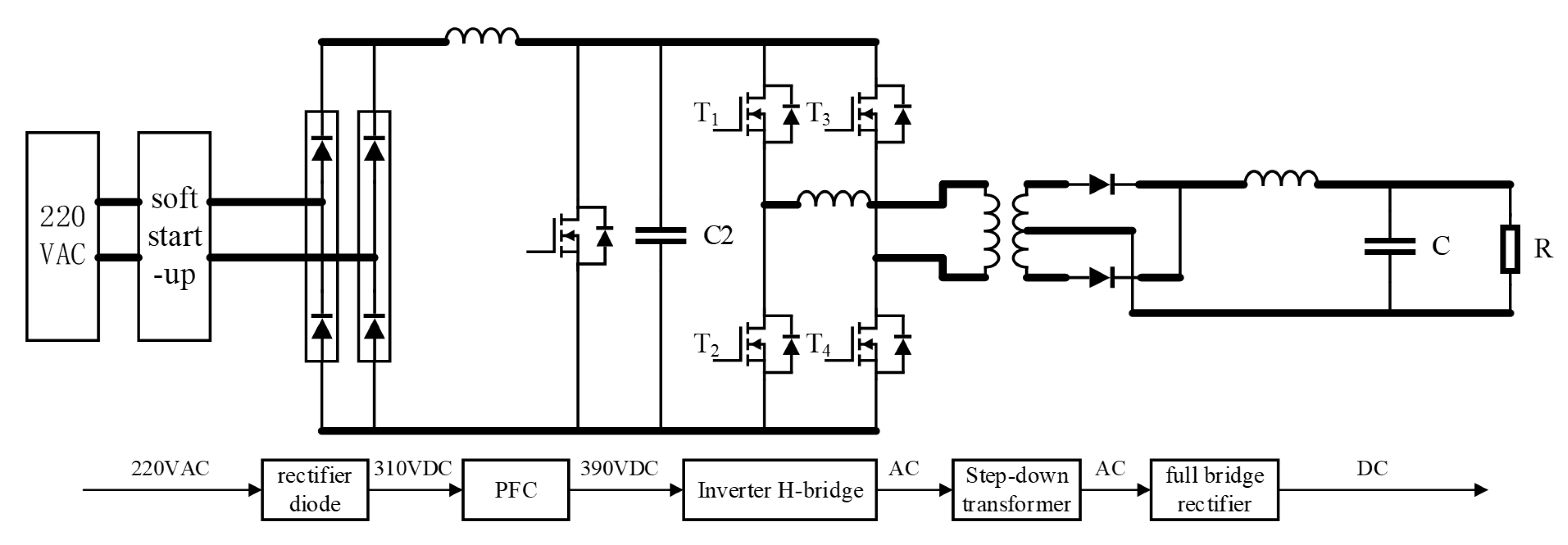
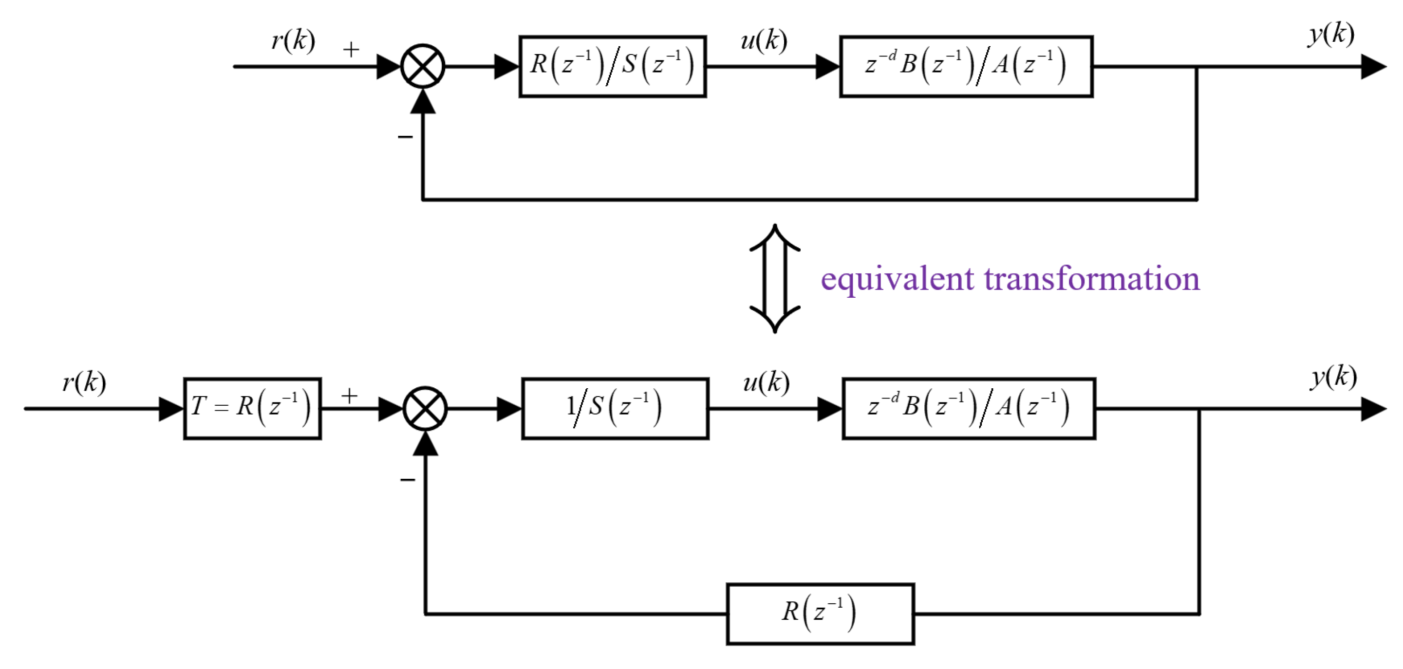
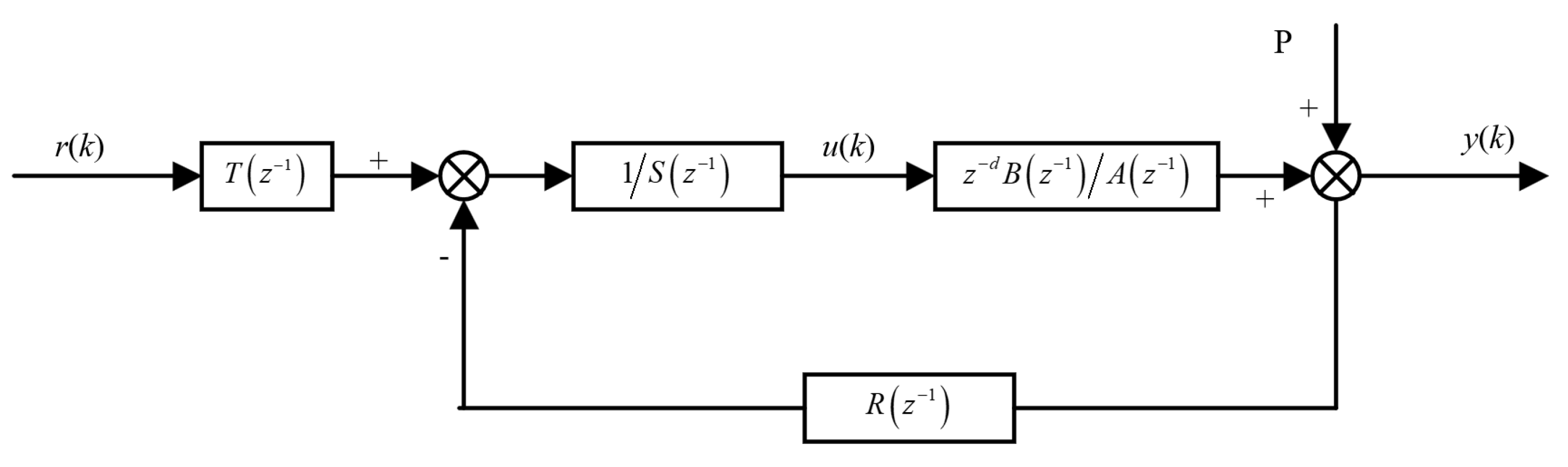
2. Reliability Design and Control Method of the Charging System

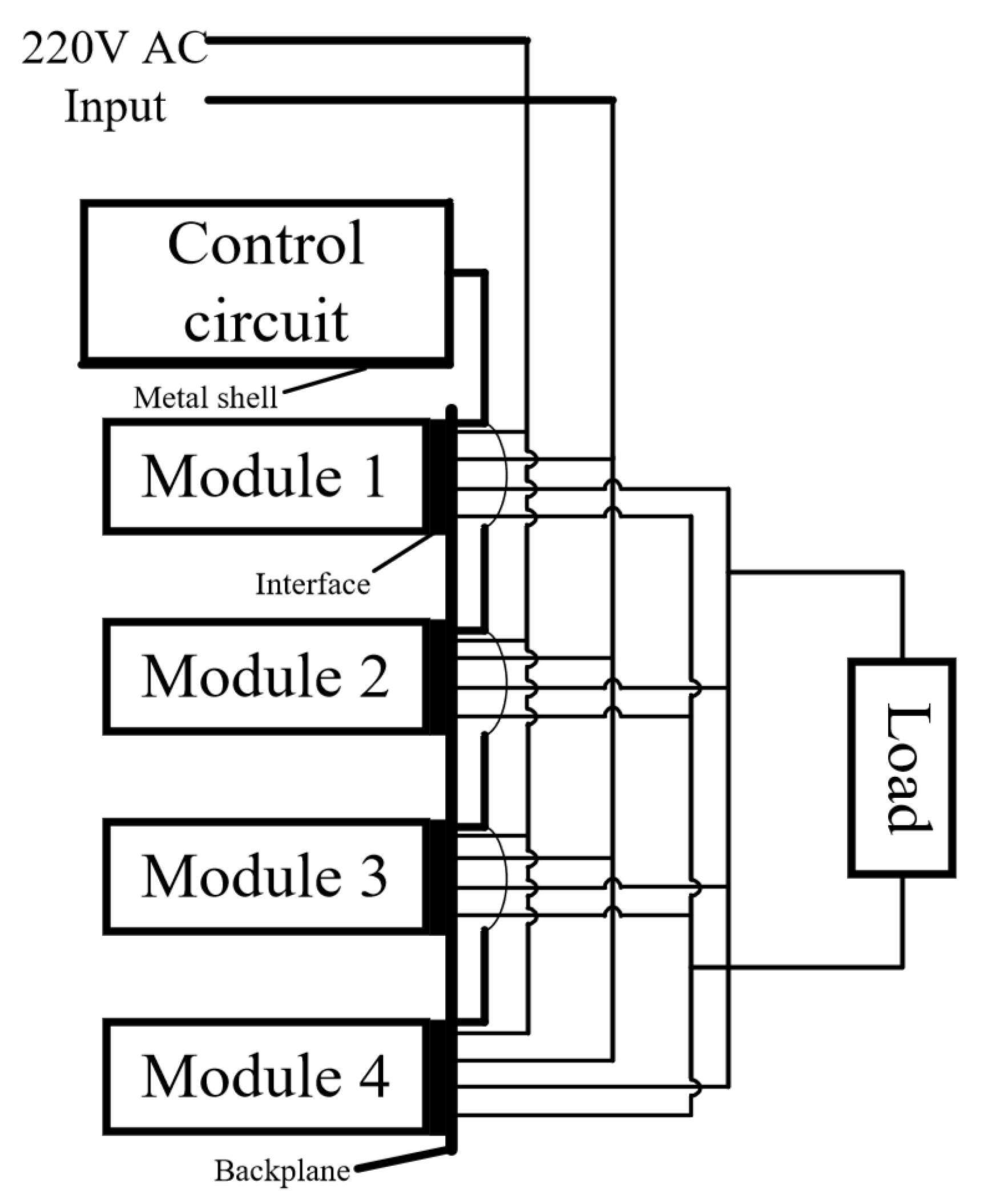
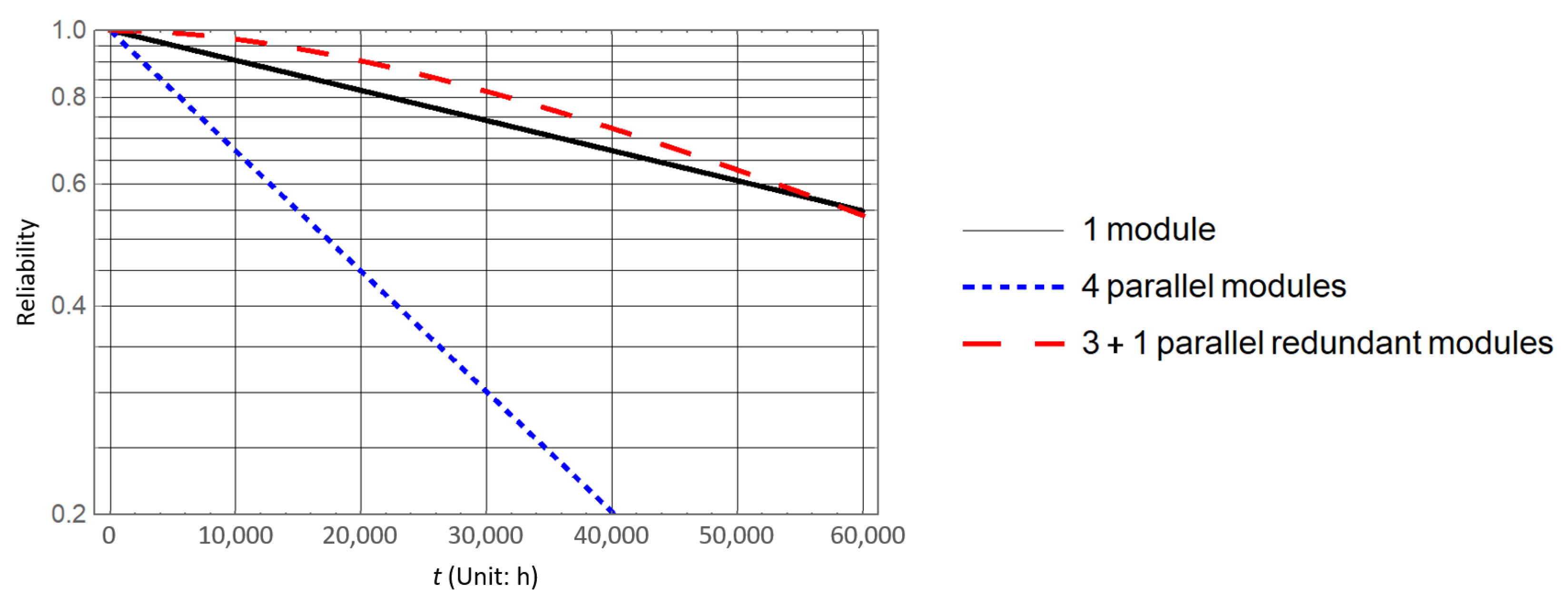
2.1. Reliability Design and Analysis of Charging System Structure

Four converter modules are connected in parallel, and any of the modules in this 3 + 1 structure can be used as the redundant module. The control circuit is arranged in a separate control box, and the control box uses a metal layer to shield the interference signals from converter modules, as shown in Figure 1.
Each power module in Figure 1 is an independent current source since voltage sources are not allowed to be connected in parallel. The fault-tolerant process is as follows: Normally, each module is operated at less than the rated current. This derating operation can reduce power consumption and operating temperature, thus improving reliability. When any one of the modules fails, the remaining three modules will quickly increase their current to make up for the current loss of the power supply due to module failure and operate at rated power, and the total output current of the charging system can be restored to the state before the failure. We analyze the reliability of the N + 1 system as follows.
Reliability is defined as the ability of a product to perform a specified function under specified conditions and within a specified period time. Mathematically, we express it in the form of a probability, which indicates the degree of completion of a certain function. The lives of most electronic components follow an exponential distribution (the failure rates are constant) and their reliabilities are as follows [36].
R ( t ) = e 0 t λ ( t ) d t = e λ t
where λ is the failure rate of the components and its unit is Fit, 1 Fit = 10 9 /h.
The reliability model of each module of the charging system is mostly a series model (i.e., failure of any one important single point will lead to the failure of the whole module), and its reliability is:
R m ( t ) = i = 1 n R i ( t ) = i = 1 n e 0 t λ i ( t ) d t = i = 1 n e λ i t = e i = 1 n λ i t = e λ m R t
where R i ( t ) is the reliability of the ith component; λ i is the failure rate of the ith component, and λ m R is the failure rate of a single module operating at rated power. If a power supply containing four parallel modules does not have any redundant modules, its reliability model is the series reliability of four modules.
R s 4 ( t ) = e 4 λ m R t = e λ m R t 4 = R m ( t ) 4
If one of the four modules is redundant, the charging system is a 3 + 1 system, and in addition, the N + 1 power failure rate is approximately proportional to its operating power [37], and λ mO = N λ mR N λ mR N + 1 N + 1 when the module is operating at derating power of NP/(N + 1). The reliability is as follows.
R s ( t ) = ( 3 + 1 ) e 3 λ mO t 3 e ( 3 + 1 ) λ mO t = ( 3 + 1 ) e 3 2 ( 3 + 1 ) λ m R t 3 e 3 λ m R t
where R s ( t ) is the module reliability of the charging system; λ mO is the failure rate of the module of the charging system at the actual operating power.
To illustrate the reliability benefits of the N + 1 system more intuitively, we first assume that the MTBF of a module is about 10 years, which is set to 10 5 h. Figure 2 shows the reliabilities of a single module, a system without redundancy, and the 3 + 1 redundant system over time, respectively.
The graph shows that the reliability of the parallel redundant system with 3 + 1 modules is much higher than the reliability of the system without redundancy and even higher than the reliability of individual modules at 55,000 h. The reliability performance is very good.
Then, we need to design the topology of each module. Since most EV charging systems are high-power systems, we tried our best to make the power of the prototype as high as possible and design each module to 1000 W (50 V/20 A). At the input side, we add a PFC BOOST circuit to improve the power factor and power of the module. At the output side, we use a transformer to achieve voltage reduction and isolation, the low-voltage output is important for experimenter safety. At the main side of the transformer, we need to design an H-bridge to change the DC power to alternating current (AC) so that the power can be transmitted through the transformer. This also prepares the ground for the realization of ZVS. We use a phase-shifted full bridge (PSFB) for zero voltage switching (ZVS), which can greatly reduce the temperature of the transistor during operation. The topology of the power module is shown in Figure 3.

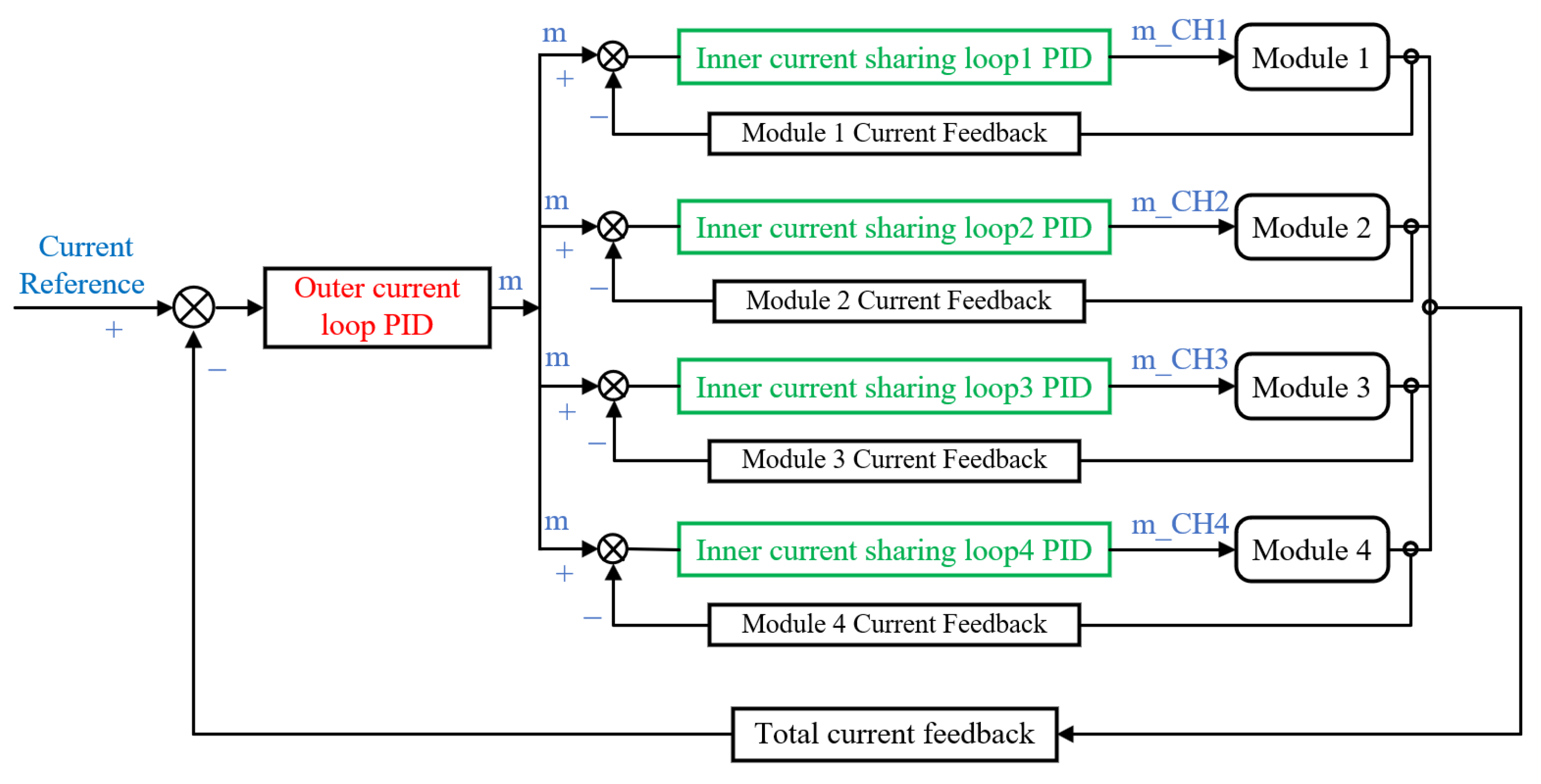
2.2. FPGA-Based Control Design for Redundancy and Fault Tolerance

We design the thermal sharing control method based on current sharing control. To help us make sense of thermal sharing, we first describe the idea of current sharing control for parallel modules as follows. Double closed-loop control is designed. The outer loop is a current loop that stabilizes the output current of the charging system, and the four inner loops are used to achieve current sharing, each module can be adjusted independently, and the amplitudes and phases of the modules must be consistent to reduce the loop current between the modules. The output of the outer loop is the reference of the inner loops. The control schematic is shown in Figure 4. Four modules are connected in parallel, and m is the output of the outer-loop PID regulator, whose value is equal to the PWM duty cycle, which is used as a common reference value for the four inner loops to obtain equal current for the four modules. Since the charging systems are current sources, both the outer and inner loop feedback signals are current. To ensure that the system can operate stably, the cutoff frequency of the inner loop needs to be much higher than that of the outer loop. We set the inner loop response speed to more than 10 times that of the outer loop so that the output of the outer loop can be approximately constant for the inner loop regulator.
We add temperature feedback in the thermal design to make the temperature of each module consistent so that the components that are subjected to high stress and more severe working conditions are subjected to less current, and finally, the temperature of the four modules is approximately the same to achieve the purpose of improving reliability. The thermal sharing control requires the addition of temperature sensors and signal feedback circuits based on the current sharing hardware platform, and the temperature sensor should be placed near the transistor to better monitor the transistor temperature fluctuations.
There are two ideas for the thermal sharing control. The first idea is to replace the current sharing loop completely with the thermal sharing loop. The outer current loop remains unchanged, the original inner current sharing loop is removed, and all four feedback physical quantities are taken as the temperature of the four modules. This control method needs to solve at least two problems: first, the relation between temperature and current—this non-linear relation is very complicated because of the complex factors involved in heat generation, heat dissipation conditions, etc. However, it can be obtained by non-linear fitting to the actual measurement results, provided that sufficient accuracy is guaranteed, otherwise, it may cause oscillations. Second, the rate of change of the temperature signal lags far behind the current signal, such as when the charging system starts to ramp up, the current can quickly follow the reference PWM to respond, but the temperature cannot be changed in time, so the feedback is very small, resulting in the given quick ramping up to the maximum value, causing an overcurrent. Perhaps this can be adjusted by adding a delay or integration parameter, but the accuracy is hard to guarantee.
The second idea is to keep the original current sharing control unchanged and add four inner thermal sharing loops. We were inspired by the RST algorithm [38]. The RST algorithm can be obtained by optimization of the PID algorithm. The RST algorithm is more complex than the PID algorithm, and the latter can be seen as a special form of the former. The mathematical proof is as follows.
The PID controller transfer function is as follows:
H PID s = U s E s = K p 1 + 1 T i s + T d s
The Z-transform of the controller is
H PID z 1 = K p + K i 1 1 z 1 + K d 1 z 1 = K p 1 + 1 T i 1 z 1 + T d 1 z 1
We define two polynomials R z 1 and S z 1 .
R z 1 = r 0 + r 1 z 1 + r 2 z 2 S z 1 = 1 z 1
The parameters of the above equation are as follows:
r 0 = K p 1 + 1 1 T i T i 2 T d r 1 = 1 2 T d + 1 r 2 = 1
From Equations (6)–(8), we obtain
H PID z 1 = R z 1 S z 1
We assume that the transfer function of the controlled object is z d B z 1 A z 1 . Then we get the PID control block diagram. Equation (9) corresponds to the block diagram on the upper side in Figure 5. The block diagram on the lower side in Figure 5 is an equivalent transformation of the upper figure.
Additionally, the block diagram of RST’s transfer function is as Figure 6.
Comparing Figure 5 and Figure 6, two differences can be found in that Figure 6 has a free transfer function T and a perturbation P. Let T = R and remove P, RST is equivalent to PID. For the RST algorithm, the transfer function T is set so that the output tracks the disturbance P, while R and S are responsible for the normal regulation of the circuit. In this way, the system tracking characteristics and regulation characteristics are achieved independently of each other. Temperature is a physical quantity that changes slowly, so its time constant is very large. If the classical PID algorithm is used, the PID time constant struggles to meet the requirements of both the slowly changing temperature and the rapidly changing current. Therefore, we refer to the controlling idea of RST algorithm and separate the temperature regulation and current regulation from each other. The temperature is considered as a disturbance P so that the charging system tracks the temperature change without affecting the PID regulation characteristics of the current.
In summary, in the first approach, we tried to find the relationship between temperature and current, and we did not choose this idea because of problems such as nonlinearity and hysteresis of the temperature-current relationship. The second method has more advantages and is the one we chose. Instead of converting the temperature signal directly to a current signal, we use the temperature as a form of perturbation to slowly correct the reference value of the current in the inner loop.
We will describe the specific process of control as follows. We first need to convert the analog quantities of current and temperature into digital quantities, using Hall sensors and temperature sensors, respectively. It is worth noting that because the relationship between temperature and temperature sensor is linear, the value of the temperature sensor corresponds exactly to the temperature value. The temperature sensor uses AD590, whose 0 μA corresponds to 0 K temperature, and the linear relationship between its output current and temperature is 1 μA/K. Then, we need to determine the reference value of the temperature. Since the relationship between current and temperature is not available, it is also difficult to derive the temperature modulation parameters from the current modulation parameters. However, we can choose the average temperature of the four modules as the reference value, and correct the reference values m of the four inner current sharing loops by feedback. After obtaining the digital temperatures of the 4 modules, the sum of the digital temperatures of the 4 modules divided by 4 is the average temperature. Since we choose the average temperature of the four modules as the reference value for the thermal loops, the increase and decrease of m-values of the 4 modules are equal. For the full-bridge inverter circuit, it is known that the duty cycle m and the output current are linearly related, therefore, the increase and decrease of the total current are also equal, thus, the total current is constant. Finally, we can slowly adjust the temperature of all modules to be consistent, as shown in Figure 7.
Figure 7 is obtained by improving on Figure 4. The difference between the average temperature of the four modules and the temperature of each module is adjusted by the PID regulators to make four corrections to the PWM duty cycle m which is the external loop output, and the obtained m _ CH 1 , m _ CH 2 , m _ CH 3 , and m _ CH 4 are the reference values of the four modules. As the temperature changes slowly, the temperature signal feedback process is very smooth and does not affect the stability of the current significantly.

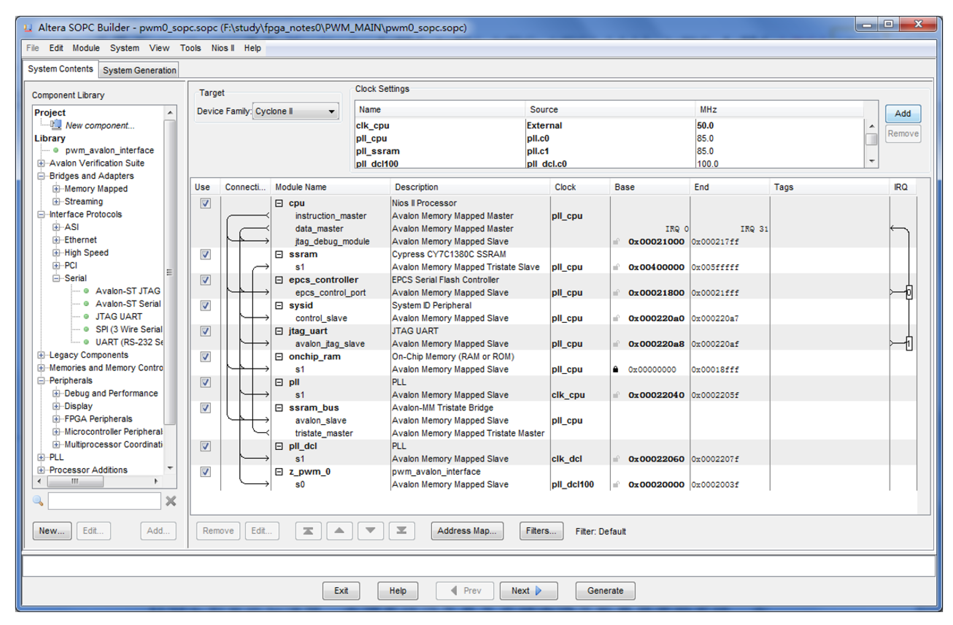
3. Development of an FPGA-Based Control System

3.1. Introduction of the Control System

The control circuit hardware uses FPGA as the core component, and other major devices include ram, flash, crystal oscillator, regulated power supplies, ADC/DAC and I/O, etc., as shown in Figure 8.
The main physical quantities are divided into analog and digital quantities. Analog quantities include the total output current and output current and temperature of each module. Digital quantities include switching signals, PWM, and fault protection signals. The sensors collect analog quantities, feed them to ADCs for AD conversion, and normalize them before computing them to generate PWM modulated PWM-modulated signal m.
We develop a system on a Programmable Chip (SOPC) based on the FPGA, adding IP cores such as CPU, memory, and interfaces to the system. The above IP cores are provided by software manufacturers and are not relevant to the key technologies in this paper, so we do not explain them in detail. We focus on explaining the user-defined logic Z _ PWM _ 0 , which includes all the key IP cores and is written in the hardware description language VHDL, as shown in Figure 9.

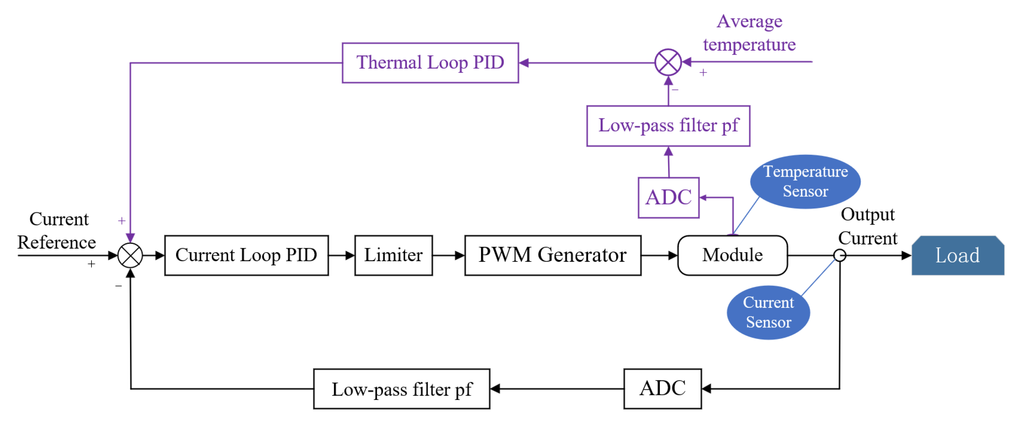
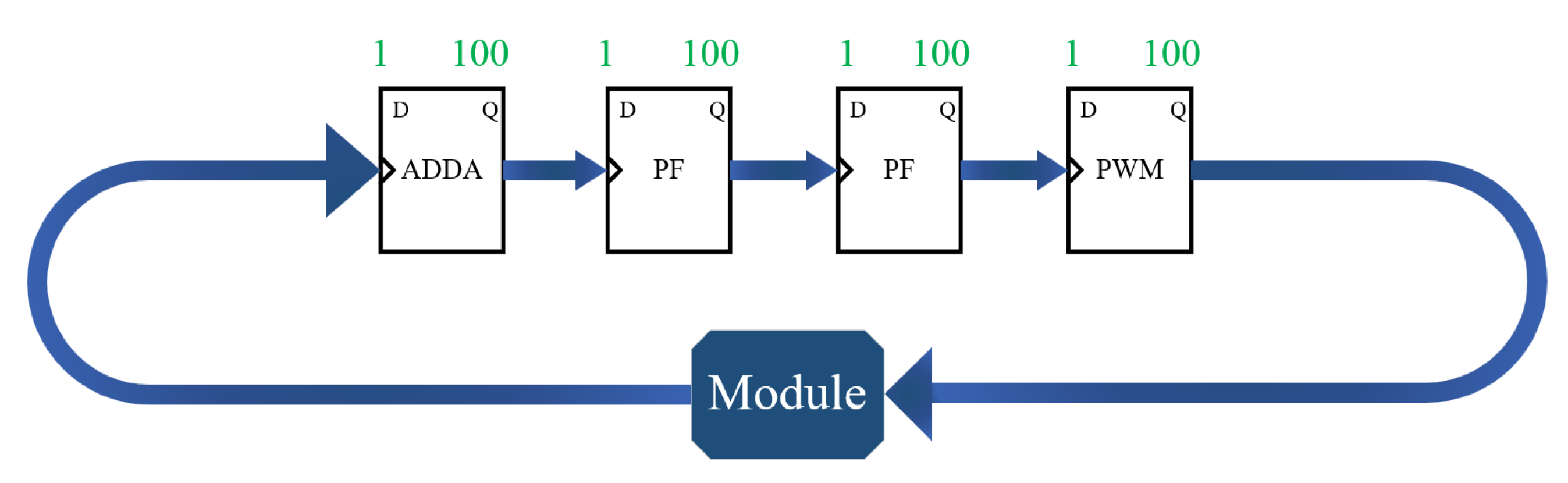
3.2. Implementation of the Main Control Logic

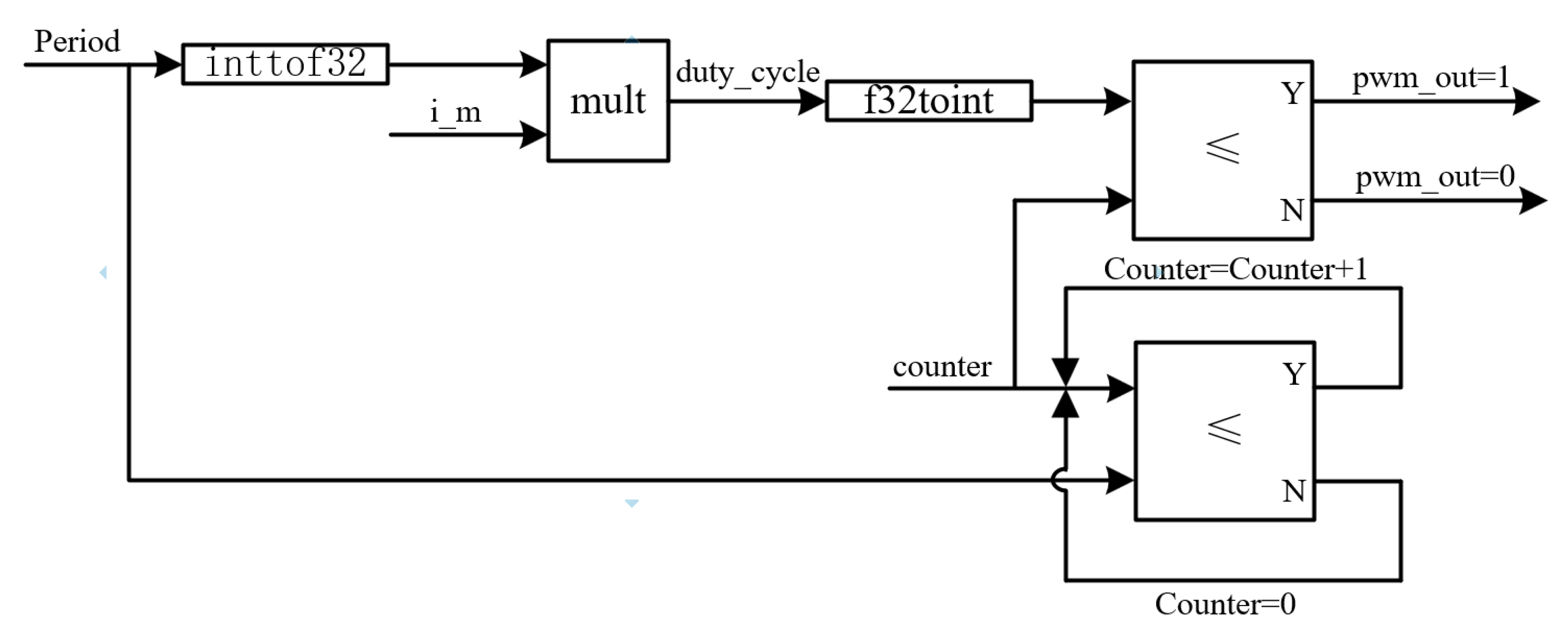
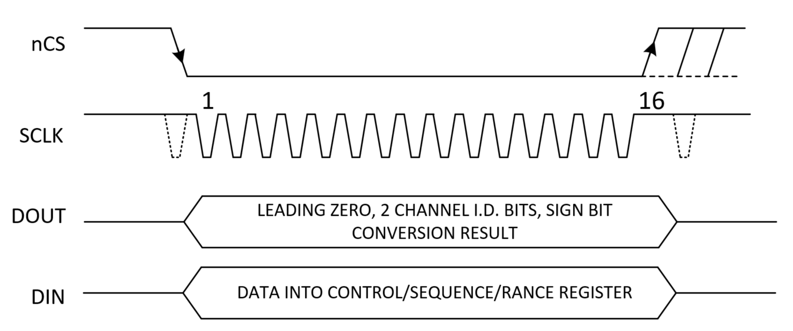
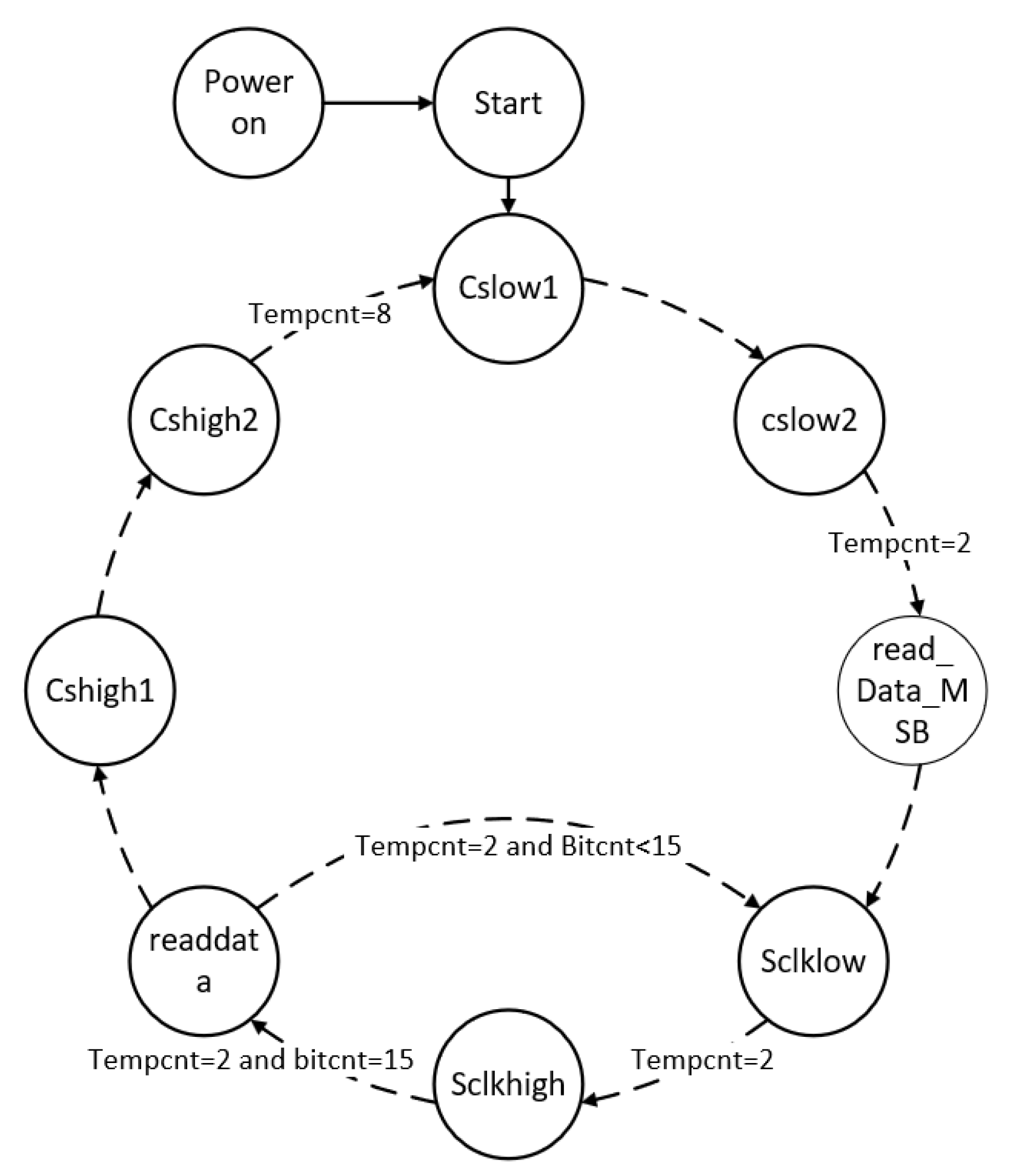
3.2.1. Main Parts of Control Logic and Pipeline Timing Processing

For a closed-loop feedback system, three elements are required: feedback signal sampling and processing, control algorithm, and drive signal generation. Tak any module in this charging system as an example, the control process is shown in Figure 10. Firstly, the current or temperature signal of the module is sampled, and after AD conversion and filtering, PID calculations are performed, and finally, the PWM signal to drive the transistor is generated. Thus, the IP cores in the user-defined logic unit Z _ PWM _ 0 mainly include the low-pass filtering pf, Control algorithm PID, PWM Generator, and ADC Driver.
For the control system design, the first thing to consider is how all the functional modules are properly interfaced. If not handled properly, it will lead to program errors. For example, we can hardly guarantee that the currents of 4 modules are processed at the same moment. Furthermore, to save computing resources, we will make repeated calls to the same IP core, for example, 4 modules call the PID IP core at 4 different times, which is not a parallel operation but a serial operation, and the 4 modules will not be synchronized, which will lead to uneven current distribution or even failure.
We propose the following solution to this problem. For Figure 10, we divide the control logic into roughly four parts, in the following order: the ADCs → low-pass filter PF → control algorithm PID → pulse generator PWM. We consider each part as a D flip-flop, and the signal inconsistency problem is solved when the previous stage transmits the data to the subsequent stage by triggering after preparing all the data. The logic clock is 100 MHz. Furthermore, 100 clocks are used as a pipeline clock Pipeline, i.e., 1 MHz, and the result is output every 1 μs, which fully meets the requirement of high-speed rate. In one Pipeline, all the operations of each stage are completed, cache the calculation results and wait, and trigger the transmission at the 100th clock, which can ensure the regular transmission of signals. The pipeline control timing diagram is shown in Figure 11.

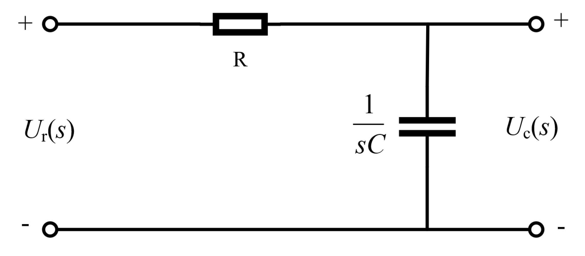
3.2.2. Logical Reasoning and Design of the Main Functions

We will elaborate on the design details of the main parts of the algorithm, including the low-pass filtering pf, the control algorithm PID, the PWM generator, and the ADC.
(1) The low-pass filtering pf.
The RC low-pass filter circuit is shown in Figure 12, a typical first-order system.
The transfer function of the RC low-pass filter circuit is
U c s U r s = 1 R C s + 1 = 1 T s + 1
The control block diagram is shown in Figure 13.
In the abose, T = RC is the time constant. The RC filter circuit is inertia with a cutoff frequency of f c = 1 / 2 π T . The differential equation is
T d u c t d t + u c t = u r t
The system developed by FPGA is a sampling-based control system, where the control process is performed digitally, so it is necessary to discretize Equation (12). The time variable t is replaced by the sampling moment kTs (Ts is the sampling period) and the differential is replaced by the incremental form as follows:
t k T s k = 0 , 1 , 2 , d u c t d t u c k u c k 1 T s
The discretization expression is obtained.
T u c k u c k 1 T s + u c k = u r k
where k is the sampling sequence number, k = 0 , 1 , 2 . . . ; is the output value of the kth sample; u r k is the input value of the kth sample; u c k 1 is the input value of the ( k 1 )th sample. The z-transform has the following properties.
Z [ u c ( k 1 ) ] = Z 1 u c ( z )
The z-transform of Equation (13) yields the following equation.
U c ( z ) = T s T + T s U r ( z ) T T + T s Z 1 U ( z )
Z 1 is the delay factor and Z 1 U ( z ) denotes the sampled value of the previous moment of U ( z ) .
The FPGA-based implementation of Equation (16) must also take into account the data type. Analog quantities are converted into digital quantities by ADC, which are integer type, but to ensure accuracy, FPGA uses floating point type for four fundamental operations. Figure 14 shows the flowchart of the FPGA-based implementation of the digital filtering pf.
Where adc_scaling indicates the inverse of the AD7324 range, and this parameter is normalized to the AD7324 output. The parameters K1 and K2 are determined by the sampling frequency Ts and the time constant T of the filter.
According to the definition of Nyquist, the cutoff frequency of the low-pass filter needs to be greater than half of the sampling frequency, so the cutoff frequency of the digital filter needs to be greater than 5 × 10 5 Hz, and since the cutoff frequency f c = 1 / 2 π T . It can be obtained that the value of K1 is in the range of [1/(1/ π + 1) ≈ 0.759, 1/(1/2 π + 1) ≈ 0.863], and the values of K2 are in the range of [1/(1/ π + 1) ≈ 0.137, 1/(1/2 π + 1) ≈ 0.241].
In addition, it is necessary to ensure that each stage completes a calculation within 100 clock cycles, as described in the previous section, we use the variable control_num to count from 0 to 99, as shown by the green numbers in Figure 14, the entire calculation took 33 clock cycles.
(2) Control algorithm PID.
The control algorithm has a significant impact on the system operating performance. For this 3 + 1 redundant system, one outer current loop and four inner current sharing loops as well as thermal sharing loops are used with PID algorithm. Since we found almost no effect of the differential parameter during the experiment, we set the differential coefficient to 0. The control block diagram is shown in Figure 15.
The PID controller transfer function is
H P I s = U s E s = K p + K i 1 s
The time domain expression is as follows:
u c ( t ) = K p e ( t ) + K i 0 t e ( t ) d t
Using the z-transform, we obtain
U ( z ) = E 1 ( z ) + E 2 ( z ) = K p E ( z ) + K i E ( z ) 1 Z 1 = K p E ( z ) + K i E ( z ) + Z 1 E 2 ( z )
where E1(z) and E2(z) are the proportional and integral terms, respectively. Figure 16 shows the FPGA-based flowchart. Finally, the PWM duty cycle i_m is generated and the i_m value is restricted to the range of 0 and 1.
(3) PWM Generator.
The variable counter is used to count the number of clocks in one cycle of the PWM. The product of the period and i_m is the duty cycle, which indicates the hold time of the high level in one PWM cycle. The FPGA flowchart of the PWM generator is shown in Figure 17.
(4) ADC Driver.
The analog current needs to be collected by the current Hall first, and the temperature signal is collected by the temperature sensor, and then the ADC is used for analog-to-digital conversion before the signal is sent to the FPGA for processing. The analog current is collected by the current Hall, the temperature signal is collected by the temperature sensor, and then the ADC is used for analog-to-digital conversion before the signal is sent to the FPGA for processing.
The analog current is collected by the current Hall, the temperature signal is collected by the temperature sensor, and then the ADC is used for analog-to-digital conversion before the signal is sent to the FPGA for processing. The ADC also needs to convert the electrical level when the power supply level of its chip is different from the electrical level of the FPGA pin. The FPGA implements control of the ADC in the form of a state machine.
We select the AD7324 chip and write values to the control register and range register of the ADC through DIN to select the range and operating mode of the chip. The timing diagram is shown in Figure 18. When the nCS signal is low, it indicates that the AD7324 enters the conversion state, and the signal is also the synchronization signal of the data frame. nCS becomes high at the end of conversion. The data is shifted out from the DOUT pin by the serial interface on the falling edge of SCLK, and the saved result can be read directly from the output register after the conversion is completed. The state machine control flow chart of ADC is shown in Figure 19.

4. Experimental Results

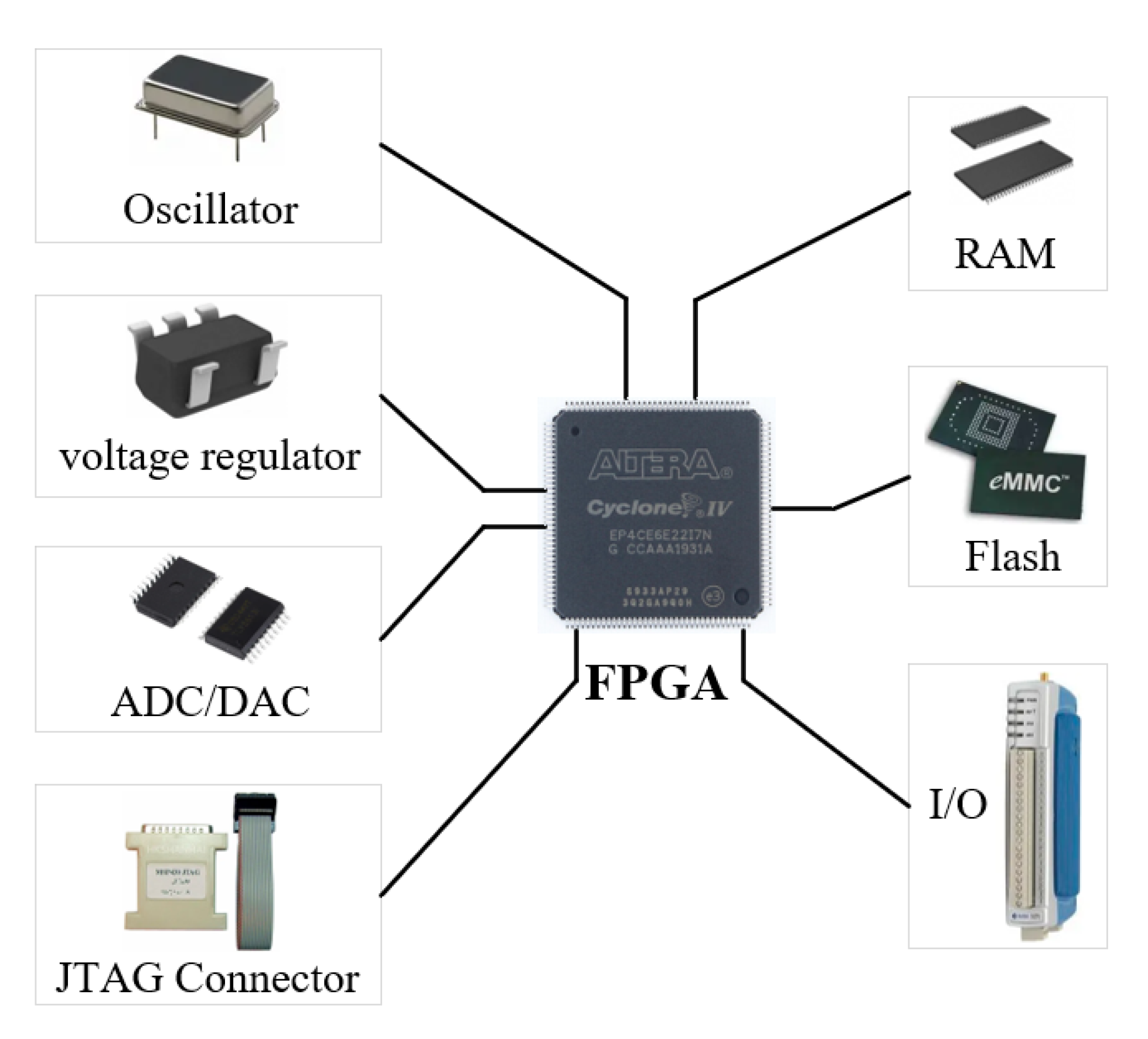
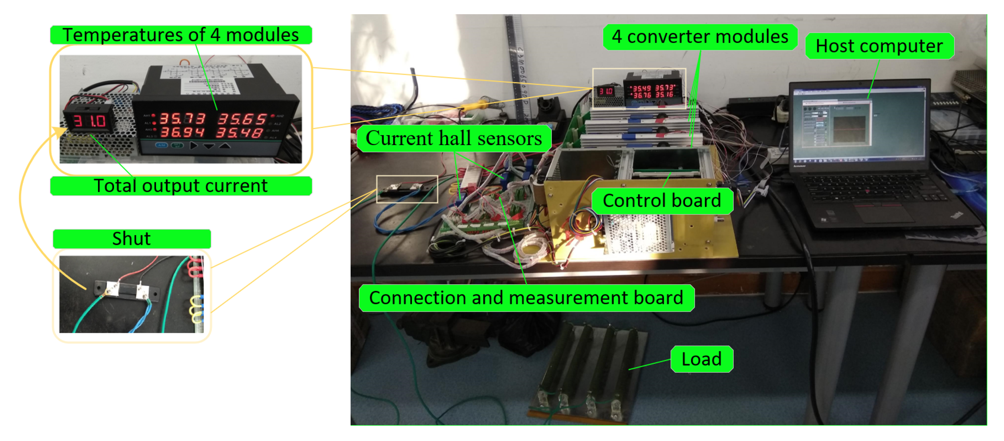
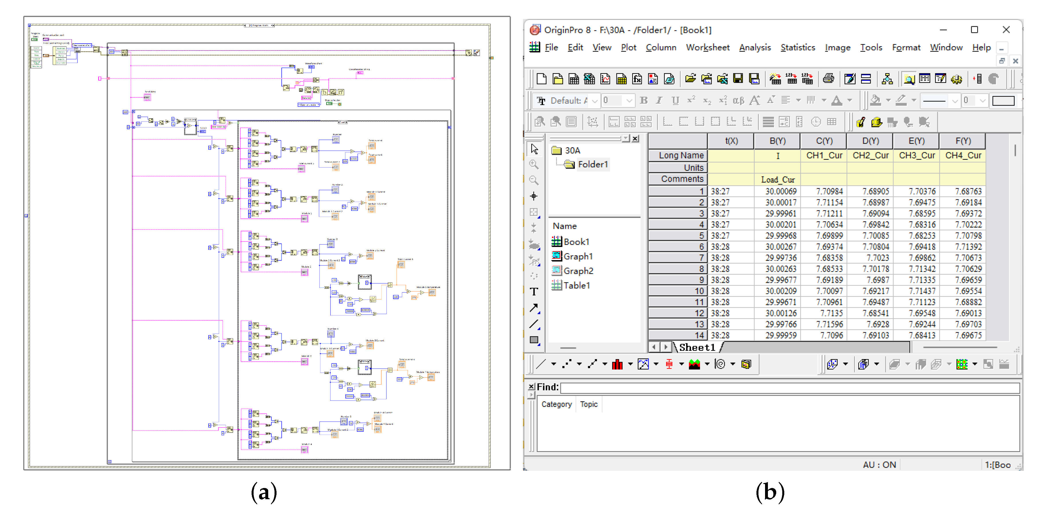
4.1. Introduction to the Experimental Platform

4.1.1. Hardware Platform

Figure 20 shows a photograph of the experimental platform.
The charging system is divided into three parts: the converter part, the control board and the connection and measurement board. The converter part is responsible for current conversion and output and consists of four modules that are connected in parallel using a backplane; The control board is responsible for the signal processing and calculations; the connection and measurement board is responsible for the communication between the converter part and the control board and current measurement. For the safety of the experimenters, we limit the output voltage to the range of 0–50 V, and the maximum output power of each module is 50 V × 20 A = 1000 W, so the maximum power of the charging system is 1000 W × 4 = 4000 W. The input voltage is single-phase 220 VAC, and the operating frequency is 50 kHz. H-bridge transistors are selected IRFP460 (500 V/20 A).
The shunt is used to measure the total current, and the temperature of the four modules is continuously monitored using a four-channel temperature display. These data are not accurate enough and are only used for observation and monitoring. The current and temperature values used for the FPGA calculations are measured by hall sensors and temperature sensors, respectively, and these values are highly accurate. Four temperature sensors are attached to the heat sink. We chose locations as close as possible to the 4 H-bridges to monitor changes in their temperatures more accurately, as the H-bridges have the highest failure rate.

4.1.2. Software Platform

It takes about 2–8 s to monitor the current changes in the charging system after a single point of failure, and 6–8 min to monitor the temperature change processes. The time is too long to be observed with an oscilloscope. Therefore, we designed a set of software programs to observe the results. First, the data are sent by FPGA to the computer through the serial port, and then the computer uses LabVIEW to read and display the data and generate the data in excel format. Finally, we used the data analysis software Origin to generate current variation waveforms from the excel data. Screenshots of the software platform are shown in Figure 21.

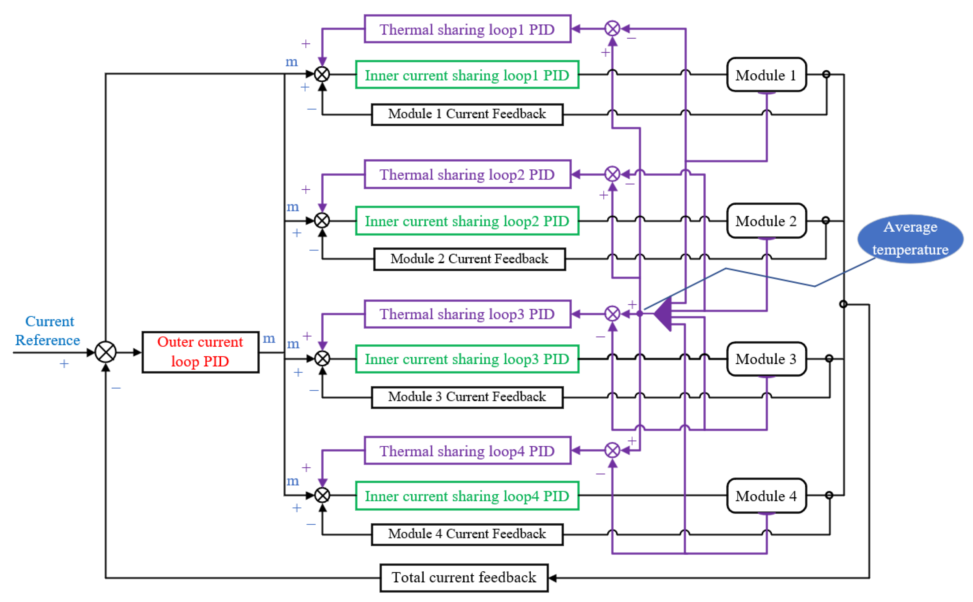
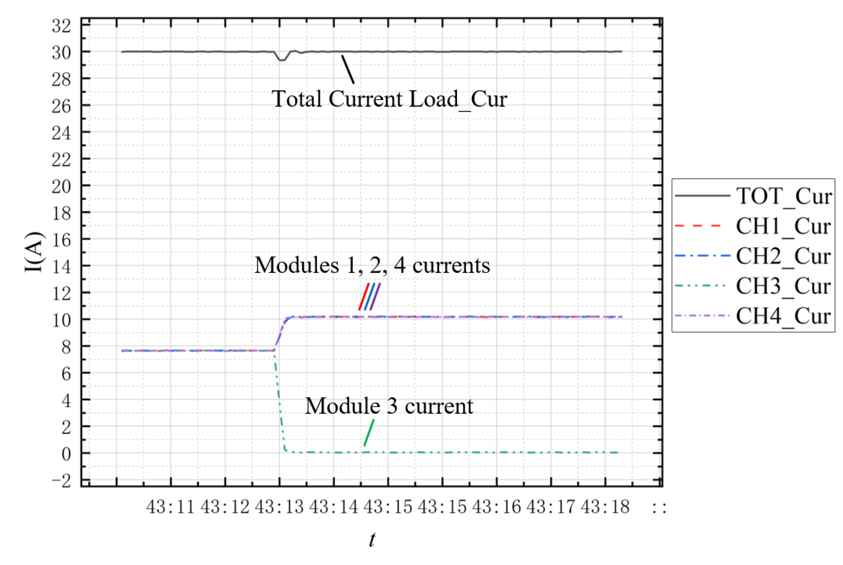
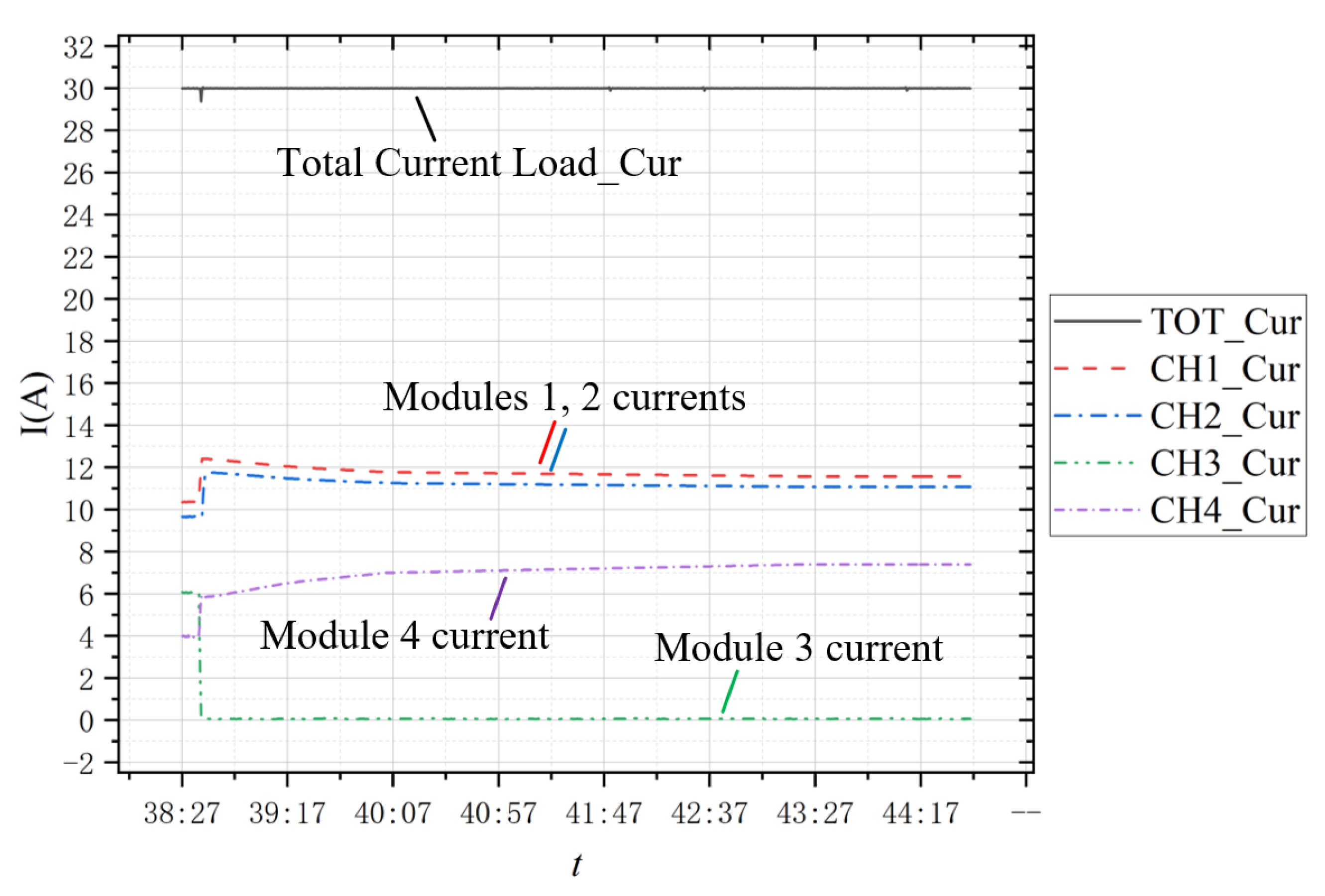
4.2. Current Sharing and Thermal Sharing Experiment

4.2.1. Current Sharing Mode

The curves were fitted accurately using the data analysis software Origin, as described above. Figure 22 shows how the current changes when the charging system achieves fault-tolerant. The red, blue, green, and purple dashed lines correspond to the current values of the first, second, third, and fourth modules, respectively. The black solid line corresponds to the total output current of the charging system. Since the charging system operates in the current sharing mode, the total output current is 30 A and the currents of all four modules are equal to 30 × 1/4 = 7.5 A during normal operation. After a module failure, the total current drop will be less than 7.5 A due to the presence of inductive circuits in the system.
We made a single point of failure to module 3 to see if the charging system could work properly. After module 3 failure, the current of module 3 rapidly drops from 7.5 A to 0 A, while the current of modules 1, 2, 4 rises from 7.5 A to 10 A. The total output current drops about 800 mA and then returns to 30 A. The total conversion time is about 500 ms. There is currently no method of achieving no fluctuation of the total current during conversion [39,40,41]. This result is excellent and shows that the structural design and the fault-tolerant control algorithm of the charging system are well. The waveform shows that the current is stable, indicating that the design idea of the control parameters in Section 2.2 is correct.

4.2.2. Thermal Sharing Mode

According to the transistor manufacturer’s datasheets, the nominal value of the MOSFET ON-resistance R DS ON can vary by as much as ±30% from one batch of transistors to another [42]. To simulate temperature differences between modules, air cooling is applied to modules 1 and 2, while no cooling is applied to modules 3 and 4.
As shown in Figure 23, before the failure, when the charging system is in a steady state, the temperature of the four modules is equal because it is in thermal sharing mode. We use I1, I2, I3, and I4 to represent the currents of modules 1, 2, 3, and 4, respectively, I1 > I2 > I3 > I4, this current difference is the result of correcting the temperature difference between modules. Additionally, the currents of modules 1, 2 are higher than the currents of modules 3, 4. This is because modules 1, 2 are air-cooled and are assigned more current in the thermal sharing mode.
When module 3 fails, the current of module 3 rapidly drops from 6 A to 0 A. As a result of the hysteresis of the temperature change, the other three modules boost the current by 2 A at the same time. Then, module 4 slowly increases the current and modules 1, 2 reduce the current due to the effect of the thermal sharing loops. This is because after the failure, modules 1 and 2 increase the temperature more than module 4, because the current of modules 1 and 2 is higher, so the same increase in 2A current but more heat. After a few minutes, the modules’ temperature stabilizes and so does the current. The experiment achieved the results we wanted and proved the correctness of our thermal sharing control method.
From the figure, we can see that although modules 1, 2, and 4 were adjusting the current after the fault occurs, it does not affect the stability of the total output current. This is because the temperature signals correct the current reference value of the inner current sharing loops, and because the temperature reference value is the average temperature, the amount of increase and decrease for the 4 inner loops is equal, so it does not affect the value of the total output current, which is consistent with the analysis in Section 2.2.

5. Conclusions

This paper presents an in-depth study on the reliability design of EV charging systems. In terms of structure, we propose a distributed charging method that has many reliability advantages over the centralized charging method currently used in electric vehicle charging stations. We designed the hardware platform of a 3 + 1 parallel modules redundant structure which can greatly improve the reliability of the system and supports both current sharing and thermal sharing modes. Additionally, we proposed a reliability evaluation method for N + 1 systems that takes fault tolerance into account; in terms of control, we have designed two control methods of current sharing and thermal sharing, and both control methods can achieve fault tolerance. The thermal sharing control can further improve the reliability of the system besides redundancy. In addition, we provide technical details of FPGA-based control algorithms and present pipeline control ideas and mathematical logic control processes. The effectiveness of the thermal sharing is determined by the temperature difference between the modules. If the quality and environment of the system are stable and the temperature difference during operation is small, it is not necessary to use the thermal sharing operation method. The future extension of the technology proposed in this paper is as follows:
(1) This paper provides a preliminary design idea for improving the reliability of EV charging stations. Further research can be conducted. It can also be further investigated how to combine this design with EV Wireless Charging;
(2) Research techniques such as increasing the inductance of the load or compensation to reduce or even eliminate the fluctuation of the total output current waveform after a power module failure present a worthwhile research direction;
(3) Reliability testing requires operational data statistics of a large number of products or operational records over a long period time (months or years). The lack of conditions in this study is unfortunate.
In summary, the method proposed in this paper has theoretical support and mathematical proof. The experimental results prove the correctness of our proposed structure and control methods. This technology can provide some reference for the designers of EV charging stations.

Author Contributions

Conceptualization, Q.Z. and Y.X.; methodology, Q.Z.; software, Q.Z., C.Y. and F.L.; validation, Q.Z.; formal analysis, Q.Z., Y.X. and T.H.; investigation, Q.Z., T.H. and C.Y.; resources, J.R. and C.Y.; data curation, J.R. and F.L.; writing—original draft preparation, Q.Z.; writing—review and editing, Q.Z., Y.X., T.H. and F.L.; visualization, J.R. and F.L. supervision, Y.X.; project administration, Y.X.; funding acquisition, Q.Z. All authors have read and agreed to the published version of the manuscript.

Funding

This research was funded by The Natural Science Foundation of Shaanxi Province, China grant number D5110220135 and The Nature Science Foundation of Shaanxi under Grant 2022JQ-653 and The Fundamental Research Funds for the Central Universities, Northwestern Polytechnical University grant number D5000210767.

Data Availability Statement

Not applicable.

Acknowledgments

We acknowledge Fengli Long of The Institute of High Energy Physics, Chinese Academy of Sciences, for her technical guidance.

Conflicts of Interest

The authors declare no conflict of interest.

References

  1. Afshar, S.; Macedo, P.; Mohamed, F.; Disfani, V. Mobile charging stations for electric vehicles—A review. Renew. Sustain. Energy Rev. 2021, 152, 111654. [Google Scholar] [CrossRef]
  2. Haines, D.J. Practical Reliability Engineering - Fifth edition. Aeronaut. J. 2012, 116, 565–566. [Google Scholar] [CrossRef]
  3. Lüdeke, A. Accelerator Reliability Reporting at the Swiss Light Source. In Proceedings of the 5th International Particle Accelerator Conf. (IPAC’14), Dresden, Germany, 15–20 June 2014; pp. 3819–3821. [Google Scholar]
  4. Kalla, U.K.; Shukla, T. State of Art and Comprehensive Study on Charging Systems for Electric Vehicles. In Proceedings of the 2021 International Conference on Sustainable Energy and Future Electric Transportation (SEFET), Virtual, 21–23 January 2021; pp. 1–6. [Google Scholar]
  5. Piasecki, S.; Zaleski, J.; Jasinski, M.; Bachman, S.; Turzyński, M. Analysis of AC/DC/DC Converter Modules for Direct Current Fast-Charging Applications. Energies 2021, 14, 6369. [Google Scholar] [CrossRef]
  6. Rahmani, F.; Niknejad, P.; Agarwal, T.; Barzegaran, M. Gallium nitride inverter design with compatible snubber circuits for implementing wireless charging of electric vehicle batteries. Machines 2020, 8, 56. [Google Scholar] [CrossRef]
  7. Wang, B.; Dehghanian, P.; Wang, S.; Mitolo, M. Electrical safety considerations in large-scale electric vehicle charging stations. IEEE Trans. Ind. Appl. 2019, 55, 6603–6612. [Google Scholar] [CrossRef]
  8. Kilic, E.; Akil, M.; Bayindir, R.; Sebati, A.; Malek, R. Electric Vehicles Charging Management with Monte Carlo Simulation. In Proceedings of the 2021 10th International Conference on Renewable Energy Research and Application (ICRERA), Ankara, Turkey, 26–29 September 2021; pp. 423–427. [Google Scholar]
  9. Bhatti, A.R.; Salam, Z. A rule-based energy management scheme for uninterrupted electric vehicles charging at constant price using photovoltaic-grid system. Renew. Energy 2018, 125, 384–400. [Google Scholar] [CrossRef]
  10. Qin, W.; Wu, X.; Zhang, J. A family of DC transformer (DCX) topologies based on new ZVZCS cells with DC resonant capacitance. IEEE Trans. Power Electron. 2016, 32, 2822–2834. [Google Scholar] [CrossRef]
  11. Qi, F.; Wang, Z.; Wu, Y.; Zuk, P. GaN FETs Enable High Frequency Dual Active Bridge Converters for Bi-directional Battery Chargers. In Proceedings of the 2020 IEEE Applied Power Electronics Conference and Exposition (APEC), New Orleans, LA, USA, 15–19 March 2020; pp. 1038–1043. [Google Scholar]
  12. Choi, H.-J.; Jung, S.-H.; Jung, J.-H. A Novel Switching Algorithm to improve Efficiency at light load conditions for Three-Phase DAB Converter in LVDC Application. In Proceedings of the 2018 International Power Electronics Conference (IPEC-Niigata 2018-ECCE Asia), Niigata, Japan, 20–24 May 2018; pp. 383–387. [Google Scholar]
  13. Zhang, W.; Xu, D. Fault analysis and fault-tolerant design for parallel redundant inverter systems in case of IGBT short-circuit failures. IEEE J. Emerg. Sel. Top. Power Electron. 2018, 6, 2031–2041. [Google Scholar] [CrossRef]
  14. Kumar, G.K.; Elangovan, D. Review on fault-diagnosis and fault-tolerant for DC–DC converters. IET Power Electron. 2020, 13, 1–13. [Google Scholar] [CrossRef]
  15. Wang, H.; Pei, X.; Wu, Y.; Kang, Y. A general fault-tolerant operation strategy under switch fault for modular series–parallel DC–DC converter. IEEE J. Emerg. Sel. Top. Power Electron. 2020, 9, 872–884. [Google Scholar] [CrossRef]
  16. Bellomo, P.; Macnair, D.; Menlo, S. SLAC Next-Generation High Availability Power Supply; Accelerator Reliability Workshop: Menlo Park, CA, USA, 26–30 January 2009. [Google Scholar]
  17. Takahashi, T.; Onda, K.; Kanouda, A.; Sato, M.; Horie, H.; Hayashi, K. Power Supply System for Supplying Electric Power to a Load through Plural Converters. U.S. Patent 5,768,117, 16 June 1998. [Google Scholar]
  18. Choudhary, V.; Ledezma, E.; Ayyanar, R.; Button, R.M. Fault tolerant circuit topology and control method for input-series and output-parallel modular DC-DC converters. IEEE Trans. Power Electron. 2008, 23, 402–411. [Google Scholar] [CrossRef]
  19. Frivaldsky, M.; Spanik, P.; Morgos, J.; Pridala, M. Control strategy proposal for modular architecture of power supply utilizing LCCT converter. Energies 2018, 11, 3327. [Google Scholar] [CrossRef] [Green Version]
  20. Zhao, N.; Liu, J.; Shi, Y.; Yang, J.; Zhang, J.; You, X. Mode analysis and fault-tolerant method of open-circuit fault for a dual active-bridge DC–DC converter. IEEE Trans. Ind. Electron. 2019, 67, 6916–6926. [Google Scholar] [CrossRef]
  21. Gosselin, C.; Schreiber, L.-T. Redundancy in parallel mechanisms: A review. Appl. Mech. Rev. 2018, 70, 010802. [Google Scholar] [CrossRef]
  22. Zhang, Z.; Meyer, E.; Liu, Y.-F.; Sen, P.C. A nonisolated ZVS self-driven current tripler topology for low-voltage and high-current applications. IEEE Trans. Power Electron. 2010, 26, 512–522. [Google Scholar] [CrossRef]
  23. Batarseh, I.; Siri, K.; Lee, H. Investigation of the output droop characteristics of parallel-connnected DC-DC converters. In Proceedings of the 1994 Power Electronics Specialist Conference-PESC’94, Taipei, Taiwan, 20–24 June 1994; pp. 1342–1351. [Google Scholar]
  24. Petruzziello, F.; Ziogas, P.; Joos, G. A novel approach to paralleling of power converter units with true redundancy. In Proceedings of the 21st Annual IEEE Conference on Power Electronics Specialists, San Antonio, TX, USA, 11–14 June 1990; pp. 808–813. [Google Scholar]
  25. Thottuvelil, V.J.; Verghese, G.C. Stability analysis of paralleled DC/DC converters with active current sharing. In Proceedings of the PESC Record, 27th Annual IEEE Power Electronics Specialists Conference, Baveno, Italy, 23–27 June 1996; pp. 1080–1086. [Google Scholar]
  26. Le Bolloch, M.; Cousineai, M.; Meynard, T. New masterless modular current-sharing technique for DC/DC parallel converters. In Proceedings of the 14th International Power Electronics and Motion Control Conference EPE-PEMC 2010, Ohrid, Macedonia, 6–8 September 2010; pp. 73–80. [Google Scholar]
  27. Du, H.; Jiang, C.; Wen, G.; Zhu, W.; Cheng, Y. Current sharing control for parallel DC–DC buck converters based on finite-time control technique. IEEE Trans. Ind. Inform. 2018, 15, 2186–2198. [Google Scholar] [CrossRef]
  28. Effler, S.; Halton, M.; Rinne, K. Efficiency-based current distribution scheme for scalable digital power converters. IEEE Trans. Power Electron. 2010, 26, 1261–1269. [Google Scholar] [CrossRef] [Green Version]
  29. Fang, W.; Liu, X.-D.; Liu, S.-C.; Liu, Y.-F. A digital parallel current-mode control algorithm for DC–DC converters. IEEE Trans. Ind. Inform. 2014, 10, 2146–2153. [Google Scholar] [CrossRef]
  30. Khaligh, A.; D’Antonio, M. Global trends in high-power on-board chargers for electric vehicles. IEEE Trans. Veh. Technol. 2019, 68, 3306–3324. [Google Scholar] [CrossRef]
  31. ElMenshawy, M.; Massoud, A. Development of modular DC-DC converters for low-speed electric vehicles fast chargers. Alex. Eng. J. 2021, 60, 1067–1083. [Google Scholar] [CrossRef]
  32. Nesgaard, C.; Andersen, M.A. Efficiency improvement in redundant power systems by means of thermal load sharing. In Proceedings of the Nineteenth Annual IEEE Applied Power Electronics Conference and Exposition, APEC’04, Anaheim, CA, USA, 22–26 February 2004; pp. 433–439. [Google Scholar]
  33. Blanks, H.S. Reliability prediction: A constructive critique of MIL-HDBK-217E. Qual. Reliab. Eng. Int. 1988, 4, 227–234. [Google Scholar] [CrossRef]
  34. Andresen, M.; Ma, K.; Buticchi, G.; Falck, J.; Blaabjerg, F.; Liserre, M. Junction temperature control for more reliable power electronics. IEEE Trans. Power Electron. 2017, 33, 765–776. [Google Scholar] [CrossRef] [Green Version]
  35. Birk, J.; Andresen, B. Parallel-connected converters for optimizing efficiency, reliability and grid harmonics in a wind turbine. In Proceedings of the 2007 European Conference on Power Electronics and Applications, Aalborg, Denmark, 2–5 September 2007; pp. 1–7. [Google Scholar]
  36. Lee, S.W.; Lee, H.K. Reliability prediction system based on the failure rate model for electronic components. J. Mech. Sci. Technol. 2008, 22, 957–964. [Google Scholar] [CrossRef]
  37. Cu, P.X.; Bui, H.A. Methodologies for reliability prediction of electronic component in military vehicles. Adv. Mil. Technol. 2019, 14, 89–98. [Google Scholar] [CrossRef] [Green Version]
  38. Abdurraqeeb, A.M.; Al-Shamma’a, A.A.; Alkuhayli, A.; Noman, A.M.; Addoweesh, K.E. RST Digital Robust Control for DC/DC Buck Converter Feeding Constant Power Load. Mathematics 2022, 10, 1782. [Google Scholar] [CrossRef]
  39. Lam, B.; Bellomo, P.; De Lira, A.; MacNair, D. ILC-ATF2 dc-magnet power supplies. In Proceedings of the 2007 IEEE Particle Accelerator Conference (PAC), Albuquerque, NM, USA, 25–29 June 2007; pp. 569–571. [Google Scholar]
  40. Wang, B.-S.; Lin, K.-B. N+ 1 redundancy power supply system by paralleling current converter modules with digital regulation control. In Proceedings of the IPAC2011, San Sebastián, Spain, 4–9 September 2011. [Google Scholar]
  41. Siemaszko, D.; Pittet, S. Failure tolerant operation and trimming principle in the CLIC main linac. In Proceedings of the 2011 14th European Conference on Power Electronics and Applications, Birmingham, UK, 30 August–1 September 2011; pp. 1–8. [Google Scholar]
  42. Nesgaard, C.; Andersen, M.A. Optimized load sharing control by means of thermal reliability management. In Proceedings of the 2004 IEEE 35th Annual Power Electronics Specialists Conference (IEEE Cat. No. 04CH37551), Aachen, Germany, 20–25 June 2004; pp. 4901–4906. [Google Scholar]
Figure 1. Charging system block diagram.
Machines 10 01162 g001
Figure 2. Comparison of the reliability of the N + 1 charging system over time.
Machines 10 01162 g002
Figure 3. The topology of the module.
Machines 10 01162 g003
Figure 4. Block diagram of current control.
Machines 10 01162 g004
Figure 5. Block diagrams two forms of PID algorithm.
Machines 10 01162 g005
Figure 6. Block diagrams of RST algorithm.
Machines 10 01162 g006
Figure 7. Block diagram of thermal control.
Machines 10 01162 g007
Figure 8. Hardware block diagram of the control system.
Machines 10 01162 g008
Figure 9. Control system SOPC.
Machines 10 01162 g009
Figure 10. The control process of the module.
Machines 10 01162 g010
Figure 11. Pipeline control timing diagram.
Machines 10 01162 g011
Figure 12. Schematic of RC low-pass filter.
Machines 10 01162 g012
Figure 13. Block diagram of the low-pass filter.
Machines 10 01162 g013
Figure 14. FPGA implementation diagram of low-pass filter pf.
Machines 10 01162 g014
Figure 15. Block diagram of PID control.
Machines 10 01162 g015
Figure 16. FPGA implementation diagram of PID control algorithm.
Machines 10 01162 g016
Figure 17. FPGA implementation diagram of PWM generator.
Machines 10 01162 g017
Figure 18. Timing diagram of the ADC.
Machines 10 01162 g018
Figure 19. Schematic diagram of the state machine for the ADC.
Machines 10 01162 g019
Figure 20. 3 + 1 modules charging system experimental platform.
Machines 10 01162 g020
Figure 21. Screenshots of the software platform. (a) The sampling and display program based on the software LabVIEW; (b) Data processing based on the software Origin.
Machines 10 01162 g021
Figure 22. Current change after module 3 failure in the current sharing experiment.
Machines 10 01162 g022
Figure 23. Current change after module 3 failure in thermal sharing experiment.
Machines 10 01162 g023
Publisher’s Note: MDPI stays neutral with regard to jurisdictional claims in published maps and institutional affiliations.

