Article

Rippled Graphene as an Ideal Spin Inverter

1
MLIT, Joint Institute for Nuclear Research, 141980 Dubna, Russia
2
Institute of Experimental Physics, 04001 Košice, Slovakia
3
BLTP, Joint Institute for Nuclear Research, 141980 Dubna, Russia
4
Faculty of Natural and Engineering Science, Dubna State University, 141982 Dubna, Russia
*
Author to whom correspondence should be addressed.
Symmetry 2023, 15(8), 1593; https://doi.org/10.3390/sym15081593
Submission received: 24 July 2023 / Revised: 8 August 2023 / Accepted: 11 August 2023 / Published: 16 August 2023
(This article belongs to the Special Issue Cooperative Effects in Finite Systems)

Abstract

:
We analyze a ballistic electron transport through a corrugated (rippled) graphene system with a curvature-induced spin–orbit interaction. The corrugated system is connected from both sides to two flat graphene sheets. The rippled structure unit is modeled by upward and downward curved surfaces. The cooperative effect of N units connected together (the superlattice) on the transmission of electrons that incident at the arbitrary angles on the superlattice is considered. The set of optimal angles and corresponding numbers of N units that yield the robust spin inverter phenomenon are found.

1. Introduction

Since the discovery of spin transport in graphene, far-reaching consequences for fundamental aspects of spintronics and its potential applications were soon realized [1]. It is well understood that, in this case, applications in spintronics are sensitive dependent on the strength of spin–orbit coupling (SOC). In particular, the form of the SOC suggested by Kane and Mele [2], and by other authors [3,4,5], in freestanding graphene is too weak for practical applications. Furthermore, this form relies on the presence of external fields, which introduces additional constraints.
Noteworthy is the fact that a graphene sheet is corrugated naturally due to intrinsic strains. It is predicted that a corrugation (ripple) in a tight-binding approximation could create electron scattering in graphene, caused by the change in nearest-neighbor hopping parameters by the curvature [6,7]. It is notable that the lattice deformation changes the relative orientation of the orbitals of the corrugated graphene sheet, leading to hybridizations of the π - and σ -bonds [8]. As a result, it is shown that a one-dimensional periodic rippled nanostructure produces a strong focusing effect of ballistic electrons due to Klein tunneling. More importantly, in the low-energy physics of graphene, the mean curvature generates a curvature-induced SOC [9] without any external field. Based on this fact, it was demonstrated that curvature-induced SOC [9,10] could produce a chiral transport [11,12]. In this case, the transport of ballistic electrons through periodically repeated ripples is subject to selection rules: Depending on the direction of motion, the system is transparent only for one spin polarization. Moreover, the polarization changes to the opposite when the flow direction changes. A similar phenomenon has been discussed recently in metal-halide semiconductors (for a review, see [13]). All these predictions imply that it might be possible to control the electronic and transport properties of a graphene sheet by altering its curvature.
Experimental achievements in a spatial variation of graphene provide a sufficient basis for such reasoning. For example, ripples can be formed by means of electrostatic manipulation without any change in doping [14]. Periodically rippled graphene is fabricated by the epitaxial technique [15], and by means of the chemical vapor deposition [16]. It is discovered that ripples, acting as potential barriers, yield the localization of charged carriers [17]. Indeed, the effect of the SOC in graphene, in conjunction with the ability to control its geometry, allow for rich spin physics.
We recall that a consistent approach to introduce curvature-induced spin–orbit coupling in the low-energy physics of the carbon nanotubes (CNTs) have been developed by Ando [9] (see also [3,18,19]) in the framework of effective mass and tight-binding approximations. Experiments in ultra-clean CNTs [1,20] confirm the importance of SOC for the interpretation of the energy spectra in nanotubes. Indeed, the measured shifts are compatible with theoretical predictions [9]. On the other hand, the role of different spin–orbit terms in metallic and non-metallic CNTs is still debatable (see, for example, discussions in [21,22,23,24,25,26]). We should nevertheless point out that, at least for armchair CNTs, one obtains two SOC terms: one preserves the spin symmetry (a spin projection on the CNT symmetry axis), while the second one breaks this symmetry [9,10,24,25]. Note that the contribution of the second term was underrated [3,9,24,25]. In this paper, we will demonstrate how the both SOC terms could be used to invert a polarized spin current with a high efficiency in a rippled graphene system.
One of the goals of this paper is to figure out symmetries, as well as elucidate the transport properties, of periodic rippled graphene nanostructures, and allow the prediction of various remarkable properties. In particular, we focus on the most general case, when a beam of ballistic electrons, propagating from a flat graphene sheet, incidents at arbitrary angle on a periodically rippled graphene structure (superlattice), and exits from the opposite side to the flat graphene sheet. The main result of the present paper is that geometrical properties of this superlattice can be used as an effective mechanism of a spin-flip phenomenon for spin-polarized current traveling between non-magnetic flat graphene contacts.

2. The Model Hamiltonian and the Eigenvalue Problem

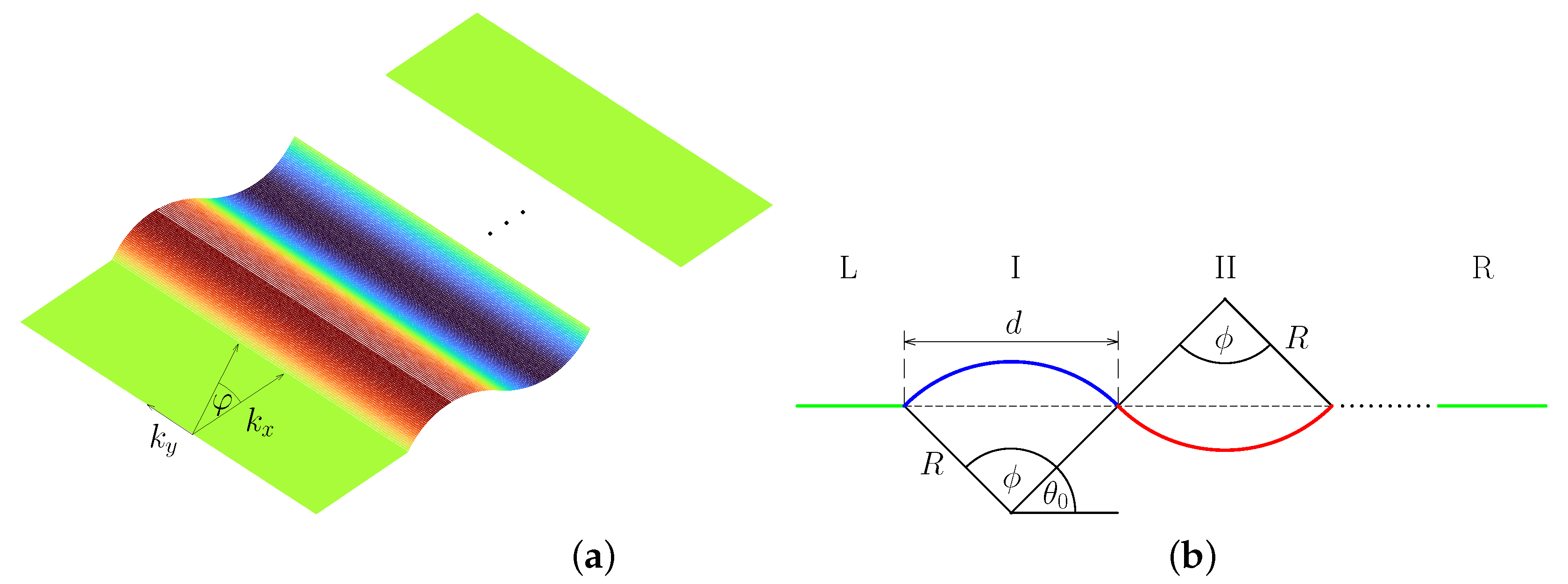
We model a corrugated graphene structure with a curved surface with periodically repeated N elements (the superlattice).
The cross section of each element consists of the curved surface perpendicular to the y axis (our quantization axis), which has the form of the direct arc of a circle (the concave surface) connected to the inverse arc (the convex surface) (see Figure 1). The first element is connected from the left side to a flat graphene sheet. Further, this structure (the first element) is repeated N times, and the last element is connected to the flat graphene sheet on the right side of our graphene structure. Hereafter, we consider a wide enough graphene sheet, keep the translational invariance along the y axis, and neglect the edge effects.
A unit cell of a honeycomb lattice contains two sublattices, called the A or B site, respectively. The effective model Hamiltonian of the flat graphene in the nearest-neighbor tight-binding model [27] has the following form:
H ^ = γ τ k I s ,
where the Pauli matrices τ x , y act on the sublattice degrees of freedom, and I s is the identity matrix of rank 2, acting in the spin space. The eigenvalues and eigenstates of the flat graphene Hamiltonian are well known (see, e.g., textbooks [28,29]):
E = κ γ k x 2 + k y 2 , κ = ± ,
Ψ k σ ( x , y ) = 1 2 κ e i φ 1 1 σ i e i k · r , σ = ± ,
where e i φ = ( k x i k y ) / k x 2 + k y 2 , k = ( k x , k y ) , r = ( x , y ) . Hereafter, we choose the up and down spins as eigenstates of the Pauli matrix σ ^ y . For the sake of convenience, we introduce the following equivalent definitions: σ = ( + / ) σ = ( / ) . The sign κ = + ( ) corresponds to the conductance (valence) band. These bands touch at two nonequivalent Dirac points (the Fermi level E = 0 ) or valleys K and K , which are at the corners of the hexagonal Brillouin zone in reciprocal space. Thus, each state is four-fold degenerate, i.e., two spin and two valley degenerate.
The solution for a curved graphene surface can be expressed in terms of the results obtained for armchair CNTs in the effective mass approximation, when only the interaction between nearest neighbor atoms is taken into account [10]. We assume that a curvature is smooth enough on the lattice scaling of graphene and does not induce the inter-valley scattering. Therefore, for the time being, we proceed our analysis for the K point.
Let us recapitulate the major results [10] in the vicinity of the Fermi level E = 0 for a point K in the presence of the curvature-induced spin–orbit interaction in an armchair CNT. In this case, the eigenvalue problem is defined as
H ^ Φ = 0 f ^ f ^ 0 F A K F B K = E F A K F B K ,
with the following definitions:
f ^ = γ ( k ^ x i k ^ y ) + i δ γ 4 R σ ^ x ( θ ) 2 δ γ p R σ ^ y , k ^ x = i R θ , k ^ y = i y , σ ^ x ( θ ) = σ ^ x cos θ σ ^ z sin θ .
Here, σ ^ x , y , z are standard Pauli matrices, and the spinors of two sub-lattices are
F A K = F A , K F A , K , F B K = F B , K F B , K .
The following notations are used: γ = 3 V p p π a / 2 = γ 0 a , γ = 3 ( V p p σ V p p π ) a / 2 = γ 1 a , p = 1 3 γ / 8 γ . The quantities V p p σ and V p p π are the transfer integrals for σ and π orbitals, respectively, in flat graphene. a = 3 2.46 Å is the length of the primitive translation vector, where is the distance between atoms in the unit cell. For numerical illustration, we assume that γ 0 3 eV and γ 1 8 eV (see, e.g., Ref. [9]). Note that by means of a similar method, we can find the solution for the K point.
The intrinsic source of the SOC δ = Δ / ( 3 ϵ π σ ) is defined as
Δ = i 3 4 m e 2 c 2 x l | V x p ^ y V y p ^ x | y l ,
where V is the atomic potential, and ϵ π σ = ϵ 2 p π ϵ 2 p σ . The energy ϵ 2 p σ is the energy of σ -orbitals, localized between carbon atoms. The energy ϵ 2 p π is the energy of π -orbitals, directed perpendicularly to the curved surface.
By means of the unitary transformation
U ^ ( θ ) = exp ( i θ 2 σ ^ y ) I ,
where I is 2 × 2 identity matrix. One removes the θ dependence in the Hamiltonian (4), transformed in the intrinsic frame, and obtains
H ^ = U ^ ( θ ) H ^ u U ^ 1 ( θ ) = H ^ kin + H ^ S O C , H ^ kin = i γ τ ^ y I y + τ ^ x I 1 R θ , H ^ S O C = λ y τ ^ y σ ^ x λ x τ ^ x σ ^ y .
Here, the operators τ ^ x , y , z are the Pauli matrices that act on the wave functions of A- and B-sublattices (a pseudo-spin space), and
λ x = γ 1 + 4 δ p / ( 2 R ) , λ y = δ γ / ( 4 R )
are the strengths of the SOC terms. The term λ x conserves, while the the term λ y breaks the spin symmetry in the Hamiltonian (9) of the armchair CNT.
The operator J ^ y , being an integral of motion H ^ , J ^ y = 0 , is defined in the laboratory frame as
J ^ y = I L ^ y + σ ^ y 2 = I i θ + σ ^ y 2 ,
while in the intrinsic frame it is
J ^ y J ^ y = U ^ J ^ y U ^ 1 = I i θ .
Finally, we obtain for the eigenvalues of Equation (4):
E = κ E ± , κ = ± 1 ,
where κ = + 1 ( 1 ) is associated with the conductance (valence) band, and the energies E ± are defined as
E ± = t m 2 + t y 2 + λ y 2 + λ x 2 ± 2 λ x 2 t m 2 + λ y 2 + t y 2 λ y 2 .
Here, t m = m γ / R , t y = γ k y , and the magnetic quantum number m = ± 1 / 2 , ± 3 / 2 , is an eigenvalue of the angular momentum operator J ^ y .
The eigenfunctions of the Hamiltonian (4) take the following form
Φ m , k y ± ( θ , y ) = e i m θ e i k y y F ± ( λ x , θ ) ,
where
F ± ( λ x , θ ) = κ ( cos θ / 2 A ± sin θ / 2 B ± ) κ ( sin θ / 2 A ± + cos θ / 2 B ± ) cos θ / 2 C ± sin θ / 2 D ± sin θ / 2 C ± + cos θ / 2 D ± ,
and
D ± = N ± λ y λ x ± λ x 2 ( t m 2 + λ y 2 ) + t y 2 λ y 2 i t m λ x t y λ y = N ± Θ ± ,
A ± = N ± E ± t m i t y + i ( λ y + λ x ) Θ ± ,
B ± = N ± E ± ( t m i t y ) Θ ± + i λ y λ x ,
C ± = N ± .
The normalization constant N ± is defined by the following expression:
N ± 2 = t y 2 λ y 2 + t m 2 λ x 2 2 λ y λ x ± λ x 2 t m 2 + λ y 2 + t y 2 λ y 2 2 + t y 2 λ y 2 + t m 2 λ x 2 .
In general, the relations | A ± | = | D ± | and | B ± | = | C ± | are fulfilled. The obtained results for the armchair CNT will be used to describe the properties of the concave and convex surface Hamiltonians.
In principle, the scattering problem that we are faced with can be considered as a scattering of a ballistic electron on two potential barriers: a scattering problem at the first barrier (the concave surface), with a subsequent scattering at the second barrier (the convex surface). Therefore, in order to resolve the eigenvalue problem for our unit, it is convenient to first solve this problem for the concave surface, and for the convex surface second.
It is convenient to describe the rippled graphene region with the concave surface ripple in the laboratory frame as half of the nanotube Hamiltonian in the following form (see Equations (4) and (5)):
H ^ u = γ ( τ ^ x k ^ x + τ ^ y k ^ y ) I s λ y τ ^ y σ ^ x ( θ ) ξ x τ ^ x σ ^ y ,
where ξ x = 2 δ γ p / R , and its eigenfunction is determined by Equation (15). In virtue of the approach developed by Ando [9], we obtain the Hamiltonian H ^ d , associated with the convex surface ripples (details will be given elsewhere):
H ^ d = γ ( τ x k ^ x + η τ ^ y k ^ y ) I s η λ y τ ^ y σ ^ x ( θ ) + ξ x τ ^ x σ ^ y ,
where, for the K-valley, we have to use η = 1 , while for the K′-valley, η = 1 . Note the transformation θ θ and ξ x ξ x in Hamiltonian (23), yields Hamiltonian (22). We found that the symmetry transformation
T ^ R = i I p e i σ ^ x π / 2 = I p σ ^ x ,
where I p is 2 × 2 identity matrix, acting in the pseudospin (sublattice) space, yields the following relation between the Hamiltonians:
H ^ d = T ^ R H ^ u T ^ R 1 .
Once the eigenproblem for the Hamiltonian (4) is solved, in virtue of the transformation (24), we can define the eigenstates for the Hamiltonian (23). Taking into account that the electron energy should be same in the concave and the convex surfaces of the unit, we have the following relations:
Φ ˜ m , k y ± ( θ , y ) = T ^ R Φ m , k y ± ( θ , y ) = e i m θ e i k y y F ± ( λ x , θ ) .
The above-described eigenfunctions (15), (26) are used to calculate the electron transmission through the curved graphene system (the superlattice) connected to the planar graphene sheets. See Section 3, below.
At a fixed value of the carrier flow E ± E ± (Equations (13) and (14)), there are four possible values of the quantum number m:
m ± = ± R γ E 2 t y 2 λ y 2 + λ x 2 2 λ x 2 ( E 2 t y 2 ) + λ y 2 t y 2 .
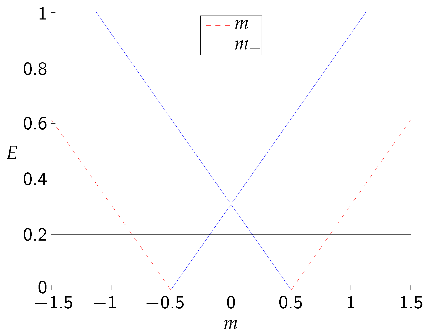
In the corrugated graphene system, the angular momentum is no longer the integral of motion. As a result, we have to consider the mixture of the eigenfunctions with all possible values at a given energy. Hereafter, we consider the positive solutions E > 0 only, since the negative solutions are symmetrically reverted.
As an example of the spectrum (14), a few positive energy branches are shown on Figure 2 as a function of the quantum number m.
For the sake of illustration, the positive energies (14) are crossed by two horizontal lines that mimic the incoming electron energies. The crossing points determine quantum numbers m that have nonquantized values when the curved surface is connected to the flat one. There is an anticrossing effect between energy states characterized by the same m + quantum number, which yields an energy gap. This anticrossing is caused by the term λ y in the Hamiltonians (22), (23), which creates the energy gap 2 λ y near the energy E = λ x at k x 0 , k y = 0 (see [10,11,12]). Let us analyze the upper and the lower limits of the energy gap, in which the evanescent modes exist in the case k x 0 , k y 0 .
Since the energy of incoming electron E = γ k x 2 + k y 2 , we have
t y = γ k y = E k y k x 2 + k y 2 = E · sin φ .
The condition of existence for evanescent modes associated with imaginary values t m is subject to the equation E + = E (see Equation (14)), such that
λ x 2 t m 2 + λ y 2 + t y 2 λ y 2 = 0 t m 2 = λ y 2 ( λ x 2 + t y 2 ) λ x 2 .
In this case, the common energy will be
E × = λ x 2 + t y 2 1 λ y 2 λ x 2 E × = λ x 2 λ x 2 cos 2 φ + λ y 2 sin 2 φ .
This equation generalizes the mid-slit position of the energy gap for the case k x 0 , k y 0 . We recall that at k y = 0 this position is determined by E × = λ x solely (see Figure 2 in Ref. [11]). Further, let us consider the situation when the energy E of the incoming electron is equal either to E + or to E . In virtue of the relation t y = E · sin φ E ± · sin φ , we obtain the following from Equation (14):
E ± = t m 2 + E ± 2 sin 2 φ + λ y 2 + λ x 2 ± 2 λ x 2 t m 2 + λ y 2 + E ± 2 λ y 2 sin 2 φ .
Squaring of the above equation yields
E ± 2 cos 2 φ t m 2 + λ y 2 + λ x 2 = ± 2 λ x 2 t m 2 + λ y 2 + E ± 2 λ y 2 sin 2 φ .
A second squaring leads us to the biquadratic equation
E ± 4 cos 4 φ 2 E ± 2 cos 2 φ t m 2 + λ y 2 + λ x 2 + 2 λ y 2 sin 2 φ + t m 2 + λ y 2 + λ x 2 2 4 λ x 2 t m 2 + λ y 2 = 0 ,
which the roots of are defined by the following equations
E + = λ x 2 cos 2 φ + λ y 2 sin 2 φ + λ y 2 + t m 2 cos 2 φ cos 2 φ ,
E = | λ x 2 cos 2 φ + λ y 2 sin 2 φ λ y 2 + t m 2 cos 2 φ | cos 2 φ .
Once the energy E = 0 , one finds that t m 2 = λ x 2 λ y 2 does not depend on φ . Thus, for the energy branch E (the dashed line in Figure 2), we obtain the following expressions as a function of t m ( m ) :
E = λ x 2 cos 2 φ + λ y 2 sin 2 φ λ y 2 + t m 2 cos 2 φ cos 2 φ , for   | t m |   0 , λ x 2 λ y 2 , λ y 2 + t m 2 cos 2 φ λ x 2 cos 2 φ + λ y 2 sin 2 φ cos 2 φ , for   | t m |   λ x 2 λ y 2 .
By means of Equation (32), it is possible to define the middle of the energy gap:
E + + E 2 = λ x 2 cos 2 φ + λ y 2 sin 2 φ cos 2 φ , for   | t m |   0 , λ x 2 λ y 2 , λ y 2 + t m 2 cos 2 φ cos 2 φ , for   | t m |   λ x 2 λ y 2 .
The “central” energy is constant for | t m |   0 , λ x 2 λ y 2 !
The energy gap between the energy branch E + and the energy branch E is defined as
E + E = 2 λ y 2 + t m 2 cos 2 φ cos 2 φ , for   | t m |   0 , λ x 2 λ y 2 , 2 λ x 2 cos 2 φ + λ y 2 sin 2 φ cos 2 φ , for   | t m |   λ x 2 λ y 2 ,
which is an increasing function at t m 0 . Indeed, the gap increases from
E + E = 2 λ y cos 2 φ at t m = 0
to
E + E = 2 λ x 2 cos 2 φ + λ y 2 sin 2 φ cos 2 φ at | t m | = λ x 2 λ y 2 .
It is notable that the energy gap at m = 0 becomes much larger with an increase in the ratio k y / k x , in comparison to the case k y = 0 . For larger t m values, the gap remains constant. The wave numbers m ± are determined by the equation
m ± = ± R γ E 2 cos 2 φ + λ x 2 λ y 2 2 E λ x 2 cos 2 φ + λ y 2 sin 2 φ ,
where E = γ k x 2 + k y 2 is the energy of incoming electron.

3. Transmission through the Superlattice

As was mentioned above, we assume that the incident ballistic electron moves from the left planar graphene sheet (L) through the superlattice to the right planar graphene sheet (R) along the x axis, and its energy is the integral of motion (see Figure 1). Hereafter, we consider a graphene sheet, in which width W along the y axis is much larger the length M along x axis, i.e., W M . In other words, we keep the translational invariance along the y axis and neglect the edge effects. By means of the continuity condition of the wave functions at the boundaries between the flat and corrugated graphene regions, we determine the unknown reflection and transmission amplitudes r α σ , t α σ ( α , σ = , ) . In these amplitudes, the upper (bottom) index denotes the spin polarization of the incoming (outgoing) (reflected and transmitted) electron.
More specifically, we have the following condition at the boundary between the regions L (the flat graphene sheet) and the concave arc (the region I, the concave surface):
A Ψ k x , k y + ( r ) + B Ψ k x , k y ( r ) + r ( L ) σ Ψ k x , k y + ( r ) + r ( L ) σ Ψ k x , k y ( r ) = a + ( 1 ) Φ m + , k y + ( θ , y ) + b + ( 1 ) Φ m + , k y + ( θ , y ) + a ( 1 ) Φ m , k y ( θ , y ) + b ( 1 ) Φ m , k y ( θ , y ) ; x = 0 , θ = π / 2 , | A | 2 + | B | 2 = 1 .
The boundary condition between the concave arc (I) and the convex arc (II) provides the following equation:
a + ( k ) Φ m + , k y + ( θ , y ) + b + ( k ) Φ m + , k y + ( θ , y ) + a ( k ) Φ m , k y ( θ , y ) + b ( k ) Φ m , k y ( θ , y ) = c + ( k ) Φ ˜ m + , k y + ( θ , y ) + d + ( k ) Φ ˜ m + , k y + ( θ , y ) + c ( k ) Φ ˜ m , k y ( θ , y ) + d ( k ) Φ ˜ m , k y ( θ , y ) x = ( 2 k 1 ) d , d = 2 R , θ = π / 2 k = 1 , , N .
Thus, regions I and II characterize two subelements of the superlattice unit, which repeats N times. Note that we have to consider the boundary condition between the region II with the next unit. Consequently, the boundary condition between the convex arc (II) and the concave arc has the following form:
c + ( k ) Φ ˜ m + , k y + ( 3 π / 2 , y ) + d + ( k ) Φ ˜ m + , k y + ( 3 π / 2 , y ) + c ( k ) Φ ˜ m , k y ( 3 π / 2 , y ) + d ( k ) Φ ˜ m , k y ( 3 π / 2 , y ) = a + ( k + 1 ) Φ m + , k y + ( π / 2 , y ) + b + ( k + 1 ) Φ m + , k y + ( π / 2 , y ) + a ( k + 1 ) Φ m , k y ( π / 2 , y ) + b ( k + 1 ) Φ m , k y ( π / 2 , y ) x = 2 k d , k = 1 , , N 1 .
Taking into account that the last Nth block, ending with the convex surface (arc) connected to the right flat graphene sheet (the region R), we obtain
c + ( N ) Φ ˜ m + , k y + ( θ , y ) + d + ( N ) Φ m + , k y + ( θ , y ) + c ( N ) Φ m , k y ( θ , y ) + d ( N ) Φ m , k y ( θ , y ) = t ( L ) σ Ψ k x , k y + ( x ) + t ( L ) σ Ψ k x , k y ( x ) x = 2 N d , θ = 3 π / 2
Eliminating the unknown coefficients a , b , c , d from Equations (36)–(39), we obtain the key equation
A B r σ r σ = M 0 ( φ ) 1 X N M 0 ( φ ) t σ t σ 0 0 ,
where the matrix M 0 ( φ ) is defined as
M 0 ( φ ) = e i φ e i φ e i φ e i φ i e i φ i e i φ i e i φ i e i φ 1 1 1 1 i i i i .
The matrix transformation X has the following structure:
X = T 1 ( ϕ / 2 ) T 2 D ( ϕ ) T 2 1 T 1 ( π ) T ˜ 2 D ( ϕ ) T ˜ 2 1 T 1 ( π + ϕ / 2 ) ,
where we introduce the following definitions
D ( ϕ ) = e i m + ϕ 0 0 0 0 e i m + ϕ 0 0 0 0 e i m ϕ 0 0 0 0 e i m ϕ ,
T 1 ( ϕ ) = cos ϕ / 2 sin ϕ / 2 0 0 sin ϕ / 2 cos ϕ / 2 0 0 0 0 cos ϕ / 2 sin ϕ / 2 0 0 sin ϕ / 2 cos ϕ / 2 ,
T 2 = A η ( λ x , m + ) A η ( λ x , m + ) A ( λ x , m ) A ( λ x , m ) B η ( λ x , m + ) B η ( λ x , m + ) B ( λ x , m ) B ( λ x , m ) C η ( λ x , m + ) C η ( λ x , m + ) C ( λ x , m ) C ( λ x , m ) D η ( λ x , m + ) D η ( λ x , m + ) D ( λ x , m ) D ( λ x , m ) ,
T ˜ 2 ( λ x , m ± ) = T 2 ( λ x , m ± ) .
In the definition (45), the following conditions hold:
  • η = 1 if E E × ;
  • η = 1 if E < E × .
The energy E × is defined by Equation (28). We consider the following situations for ballistic electrons (moving from the left flat graphene sheet and described by Equation (3)) that are incident on the superlattice with a certain polarization in Equation (40): (i) spin polarization | corresponds to the set σ = + , A = 1 , B = 0 ; and (ii) spin polarization | corresponds to the set σ = , A = 0 , B = 1 .
It is quite certain that the matrix X (Equation (42)) can be diagonalized
X v k = λ k v k ,
where λ k , v k are the eigenvalues and the eigenvectors of the matrix X, respectively. Using this fact, we transform the matrix X N into the form
X N = U λ 1 N 0 0 0 0 λ 2 N 0 0 0 0 λ 3 N 0 0 0 0 λ 4 N U 1 ,
where the matrix U
U = ( v 1 , v 2 , v 3 , v 4 )
consists of the eigenvectors { v } , and U U 1 = I .
Evidently, the eigenvalues { λ } can be written in a very general form as λ k = a k exp i ψ k , k = 1 , , 4 . Consequently, the amplitudes r α σ , t α σ ( α , σ = , ) of Equation (40) become the functions of the eigenfunctions λ k N = a k N e i N ψ k . It results in probabilities that will depend periodically on the number of units in superlattice through the functions a k ± N a j N , cos [ N ( ψ k ψ j ) ] , sin [ N ( ψ k ψ j ) ] .

4. Discussion

From the analysis of ballistic electron transport through a superlattice that consists of concave arcs (semiripples) interconnected by flat graphene sheets [30] it was shown that a periodically repeated rippled graphene structure leads to the suppression of the transmission of electrons with one spin orientation in contrast to the other, depending on the direction of the incoming electron flow. In this case, it was assumed that electrons are injected to the curved surface in a perpendicular direction, i.e., k y = 0 . In contrast to the above case, our superlattice unit contains both the convex surface connected continuously with the concave surface, and k x 0 , k y 0 .
To gain a better insight into the effect of the superlattice on ballistic transport, we numerically study its dependence on: (i) the number N of the superlattice units; (ii) the incident angle φ of ballistic electrons; and (iii) the radius of the curved surface of the unit (see Figure 1). While our approach enables us to analyze the effect for the arbitrary unit angle, in this paper, all calculations are performed for the unit angle ϕ = π . The calculation of the spin-flip probabilities are performed on the N × φ mesh with Δ N = 1 for N = 1 , , 500 units, and Δ φ = 0.01 ° for φ = 0 ° , , 50 ° . The results are shown in Figure 3 for various values of the number of N units at different values of φ = arctan k y / k x of incident electrons with an energy 0 < E 1 eV. Hereafter, we consider only the results that provide the maximal probability P N , φ 0.9999 .
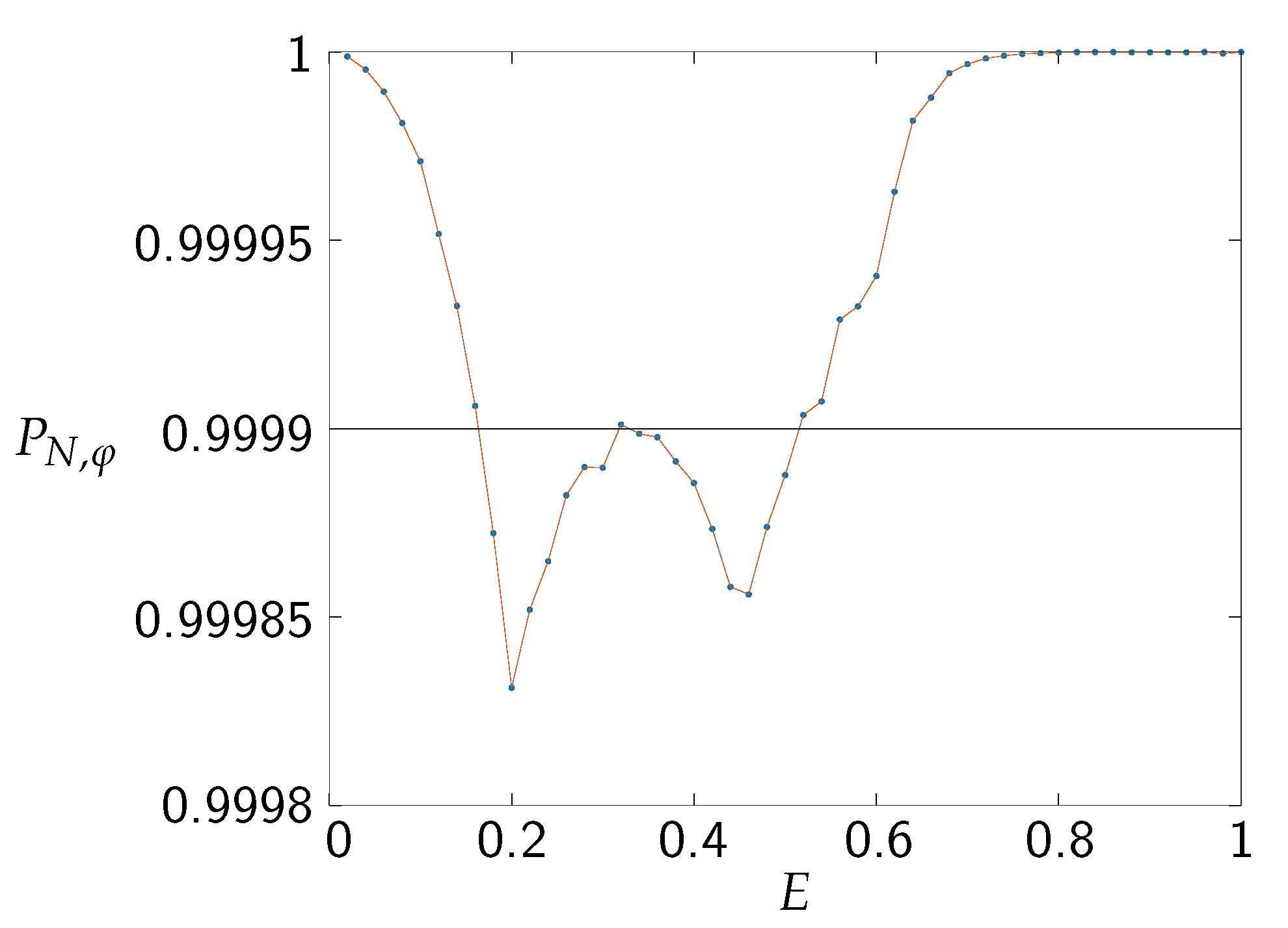
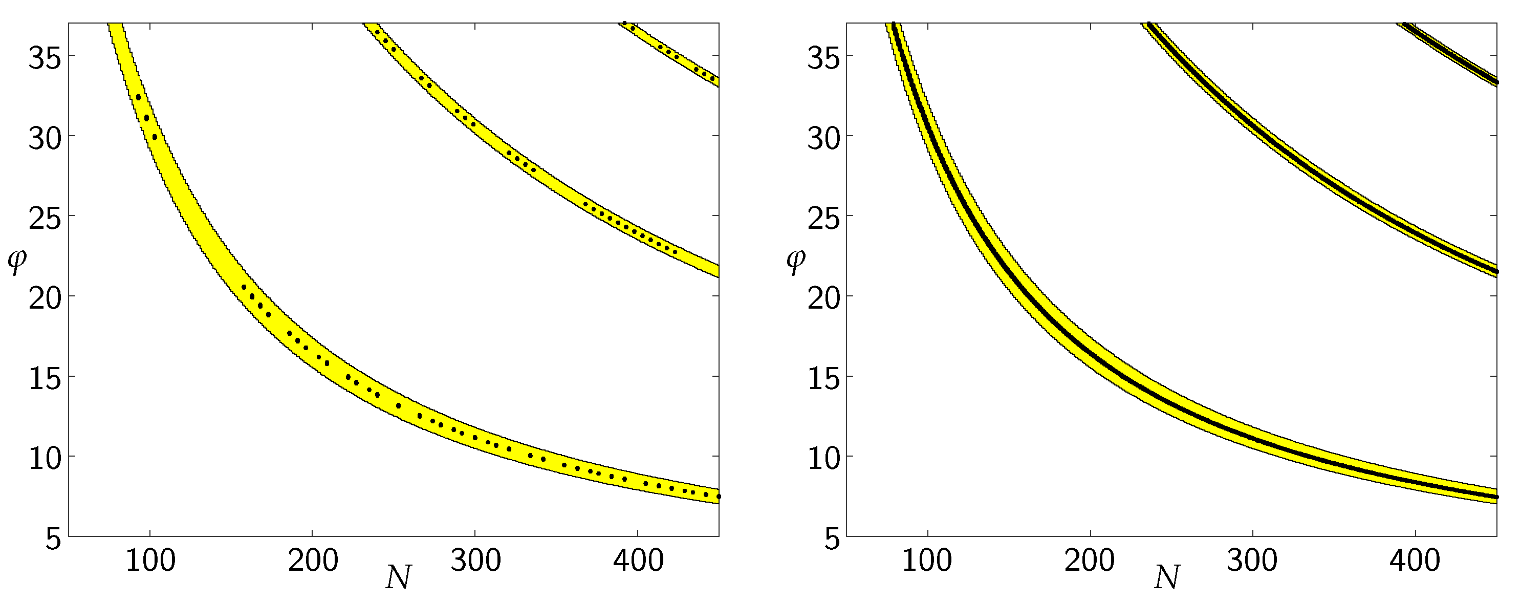
It appears that our device operates most efficiently at the incident beam energy, defined in the intervals 0 E 0.18 eV, and 0.5 E 1.0 eV (see Figure 3). In particular, at energy E = 0.1 eV (see Figure 4), we find a set of bands that provide the spin-flip effect for incident ballistic electrons for minimal N units of the superlattice. Each band is limited by the boundaries with the probability P = 0.99 . Each solid point in the band is characterized by a set { N , φ } variables that corresponds to P 0.9999 .
For example, at the incident energy E = 0.1 eV of the electron that enters to the superlattice at the angle φ = 20 ° , the latter must consist of N = 163 units to invert the polarized beam (↑ or ↓) of ballistic electrons to the opposite polarization. It is notable that, with an increase in the incident electron energy, the separate points transform to the dense points (see the right panel, Figure 4). The higher the incident electron energy, the wider the set of { N , φ } that yields the inversion effect of entrance electrons with a given polarization.
The functional dependence of the bands leads us to conclude that there is a remarkable relation
tan φ i = c i N , i = 1 , 2 , 3
that allows to determine the number of N units to obtain the maximal spin flip effect for all considered energies. The index i characterizes the band number, namely that the lowest band has the index i = 1 , etc. The least squares fitting of our results provide another interesting result
c i c 1 ( 2 i 1 )
with high accuracy, where the constant c 1 = 59.149 . It is notable that, at a given φ , it is possible to relate the number N i ( φ ) of the ripple units in the band i with the aid of the number of units N j ( φ ) in the band j and, consequently, to exclude the constant c 1 . Indeed, in virtue of relations (50)–(51), we can formulate the following result
N i ( φ ) N j ( φ ) · 2 i 1 2 j 1 N i ( φ ) N 1 ( φ ) · ( 2 i 1 ) .
As a result. we obtain the units number periodicity between the position of the maximum probabilities in different bands:
N i + 1 ( φ ) N i ( φ ) 2 N 1 ( φ ) , i = 1 , 2 ,
Thus, the knowledge of the minimal number of ripples in the first band provides the number of the superlattice units that yields the effect of the periodicity of the spin-flip phenomenon at a fixed value of the angle φ of the incident beam.
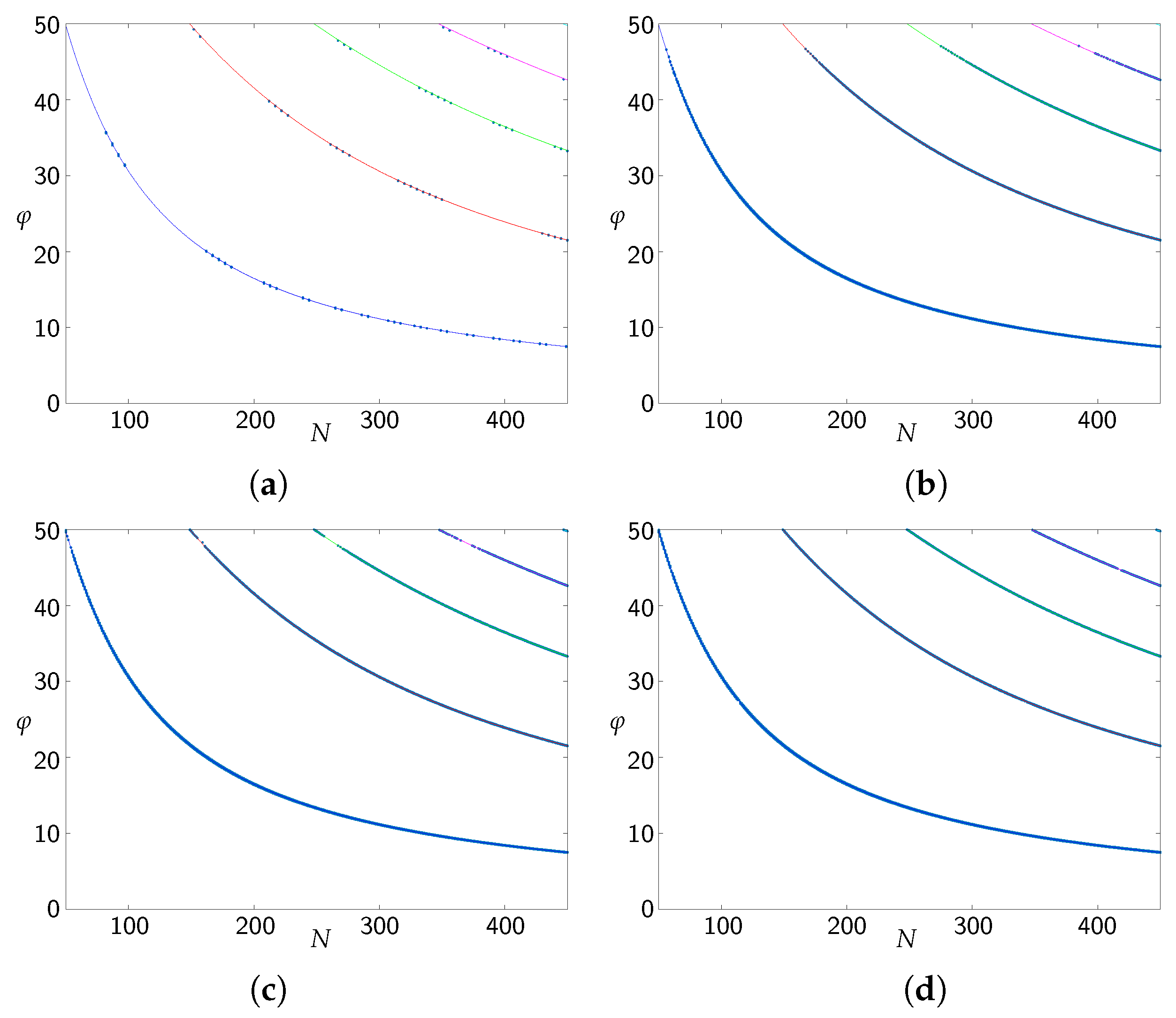
We recall that the results discussed above are valid at R = 12 Å of the ripple radius (see Figure 1b) for all considered energies. It is noteworthy that our results remain true for various values of the ripple radius as well (see Figure 5). The presence of the band structure is found for the set of different ripple radii. Although the band structures manifest themselves for a particular choice of { R , E } in the panels (a–d) in Figure 5, the results hold for all energy intervals considered in our analysis (see Figure 3) at the fixed values of the radii.

5. Conclusions

The curvature-induced spin–orbit coupling in rippled graphene structures opens a broad avenue for spintronic applications in graphene based nanodevices. In this paper, we consider the most general case of the incident angle φ = arctan k y / k x of a ballistic electron beam, injected from the plane graphene sheet on the superlattice that consists of the curved graphene units. In contrast to semiripple configurations (a concave arc) considered in [11,12,30], our superlattice consists of the concave surface continuously connected to the convex surface. This unit is repeated N times (see Section 2). The cooperative effect of our superlattice leads to almost perfect spin inversion phenomenon for the injected through this superlattice ballistic electrons with a chosen spin polarization (see Section 4) without any external field.
We found the optimal set of angles and the minimal number of corresponding N ripples (see Figure 4 and Figure 5) that yield the spin-flip operation. Such an operation (without use of the magnetic field) may be useful for production of spin-based logic elements (see [31] for a review). In particular, at a fixed energy of the injected ballistic electrons, one can choose the fixed number of ripples and obtain the spin-flip operation at specific angles of the injected electrons, i.e., the angle φ (see Figure 5d). The obvious advantages are low switching energies and low power dissipation. On the other hand, once the set { N 1 , φ i } (which provides the spin-flip operation in the first band) is chosen, this phenomenon can take place with the periodicity of 2 N 1 in the other bands (see Equation (53)). It is notable that this effect holds for all specific intervals of energies that create a type of conductance bands in the superlattice, which are independent of the ripple radius (see Figure 5). We hope that presented results could be useful for various spintronic devices once nanotechnology provides rippled graphene structures with a controlled periodicity.

Author Contributions

All authors contributed equally to this work. All authors have read and agreed to the published version of the manuscript.

Funding

This research received no external funding.

Institutional Review Board Statement

Not applicable.

Informed Consent Statement

Not applicable.

Data Availability Statement

Not applicable.

Conflicts of Interest

The authors declare no conflict of interest.

References

  1. Avsar, A.; Ochoa, H.; Guinea, F.; Özyilmaz, B.; van Wees, B.J.; Vera-Marun, I.J. Spintronics in graphene and other two-dimensional materials. Rev. Mod. Phys. 2020, 92, 021003. [Google Scholar] [CrossRef]
  2. Kane, C.L.; Mele, E.J. Quantum Spin Hall Effect in Graphene. Phys. Rev. Lett. 2005, 95, 226801. [Google Scholar] [CrossRef] [PubMed]
  3. Huertas-Hernando, D.; Guinea, F.; Brataas, A. Spin-orbit coupling in curved graphene, fullerenes, nanotubes, and nanotube caps. Phys. Rev. B 2006, 74, 155426. [Google Scholar] [CrossRef]
  4. Yao, Y.; Ye, F.; Qi, X.-L.; Zhang, S.-C.; Fang, Z. Spin-orbit gap of graphene: First-principles calculations. Phys. Rev. B 2007, 75, 041401. [Google Scholar] [CrossRef]
  5. Rashba, E.I. Graphene with structure-induced spin–orbit coupling: Spin-polarized states, spin zero modes, and quantum Hall effect. Phys. Rev. B 2009, 79, 161409(R). [Google Scholar] [CrossRef]
  6. Katsnelson, M.; Geim, A. Electron scattering on microscopic corrugations in graphene. Philos. Trans. R. Soc. A 2008, 366, 195–204. [Google Scholar] [CrossRef] [PubMed]
  7. Guinea, F.; Katsnelson, M.I.; Vozmediano, M.A.H. Midgap states and charge inhomogeneities in corrugated graphene. Phys. Rev. B 2008, 77, 075422. [Google Scholar] [CrossRef]
  8. Pudlak, M.; Nazmitdinov, R.G. Klein collimation by rippled graphene superlattice. J. Phys. Condens. Matter 2019, 31, 495301. [Google Scholar] [CrossRef]
  9. Ando, T. Spin-Orbit Interaction in Carbon Nanotubes. J. Phys. Soc. Jpn. 2000, 69, 1757–1763. [Google Scholar] [CrossRef]
  10. Pichugin, K.N.; Pudlak, M.; Nazmitdinov, R.G. Spin-orbit effects in carbon nanotubes—Analytical results. Eur. Phys. J. B 2014, 87, 124. [Google Scholar] [CrossRef]
  11. Smotlacha, J.; Pudlak, M.; Nazmitdinov, R.G. Spin transport in a rippled graphene periodic chain. J. Phys. Conf. Ser. 2019, 1416, 012035. [Google Scholar] [CrossRef]
  12. Pudlak, M.; Smotlacha, J.; Nazmitdinov, R.G. On Symmetry Properties of The Corrugated Graphene System. Symmetry 2020, 12, 533. [Google Scholar] [CrossRef]
  13. Feng, T.; Wang, Z.; Zhang, Z.; Xue, J.; Lu, H. Spin selectivity in chiral metal–halide semiconductors. Nanoscale 2021, 13, 18925–18940. [Google Scholar] [CrossRef] [PubMed]
  14. Alyobi, M.M.; Barnett, C.J.; Rees, P.; Cobley, R.J. Modifying the electrical properties of graphene by reversible point-ripple formation. Carbon 2019, 143, 762–768. [Google Scholar] [CrossRef]
  15. Vázquez de Parga, A.L.; Calleja, F.; Borca, B.; Passeggi, M.C.G.; Hinarejos, J.J.; Guinea, F.; Miranda, R. Periodically Rippled Graphene: Growth and Spatially Resolved Electronic Structure. Phys. Rev. Lett. 2008, 100, 056807. [Google Scholar] [CrossRef] [PubMed]
  16. Ni, G.X.; Zheng, Y.; Bae, S.; Kim, H.R.; Pachoud, A.; Kim, Y.S.; Tan, C.L.; Im, D.; Ahn, J.H.; Hong, B.H. Quasi-Periodic Nanoripples in Graphene Grown by Chemical Vapor Deposition and Its Impact on Charge Transport. ACS Nano 2012, 6, 1158–1164. [Google Scholar] [CrossRef] [PubMed]
  17. Vasić, B.; Zurutuza, A.; Gajić, R. Spatial variation of wear and electrical properties across wrinkles. in chemical vapour deposition graphene. Carbon 2016, 102, 304–310. [Google Scholar] [CrossRef]
  18. Entin, M.V.; Magarill, L.I. Spin-orbit interaction of electrons on a curved surface. Phys. Rev. B 2001, 64, 085330. [Google Scholar] [CrossRef]
  19. De Martino, A.; Egger, R.; Hallberg, K.; Balseiro, C.A. Spin-Orbit Coupling and Electron Spin Resonance Theory for Carbon Nanotubes. Phys. Rev. Lett. 2002, 88, 206402. [Google Scholar] [CrossRef]
  20. Kuemmeth, F.; Ilani, S.; Ralph, D.C.; McEuen, P.L. Coupling of spin and orbital motion of electrons in carbon nanotubes. Nature 2008, 452, 448–452. [Google Scholar] [CrossRef]
  21. Bulaev, D.V.; Trauzettel, B.; Loss, D. Spin-orbit interaction and anomalous spin relaxation. in carbon nanotube quantum dots. Phys. Rev. B 2008, 77, 235301. [Google Scholar] [CrossRef]
  22. Chico, L.; López-Sancho, M.P.; Muñoz, M.C. Curvature-induced anisotropic spin–orbit splitting in carbon nanotubes. Phys. Rev. B 2009, 79, 235423. [Google Scholar] [CrossRef]
  23. Jeong, V.; Lee, H.-W. Curvature-enhanced spin–orbit coupling in a carbon nanotube. Phys. Rev. B 2009, 80, 075409. [Google Scholar] [CrossRef]
  24. Izumida, W.; Sato, K.; Saito, R. Spin–Orbit Interaction in Single Wall Carbon Nanotubes: Symmetry Adapted Tight-Binding Calculation and Effective Model Analysis. J. Phys. Soc. Jpn. 2009, 78, 074707. [Google Scholar] [CrossRef]
  25. del Valle, M.; Margańska, M.; Grifoni, M. Signatures of spin–orbit interaction in transport properties. of finite carbon nanotubes in a parallel magnetic field. Phys. Rev. B 2011, 84, 165427. [Google Scholar] [CrossRef]
  26. Klinovaja, J.; Schmidt, M.J.; Braunecker, B.; Loss, D. Carbon nanotubes in electric and magnetic fields. Phys. Rev. B 2011, 84, 085452. [Google Scholar] [CrossRef]
  27. Wallace, P.R. The Band Theory of Graphite. Phys. Rev. 1947, 71, 622–634. [Google Scholar] [CrossRef]
  28. Katsnelson, M.I. Graphene: Carbon in Two Dimensions; Cambridge University Press: Cambridge, UK, 2012. [Google Scholar]
  29. Foa Torres, L.E.F.; Roche, S.; Charlier, J.-C. Introduction to Graphene-Based Nanomaterials: From Electronic Structure to Quantum Transport; Cambridge University Press: Cambridge, UK, 2014. [Google Scholar]
  30. Pudlak, M.; Nazmitdinov, R.G. Spin-dependent electron transmission across the corrugated graphene. Physica E 2020, 118, 113846. [Google Scholar] [CrossRef]
  31. Ghising, P.; Biswas, C.; Lee, Y.H. Graphene Spin Valves for Spin Logic Devices. Adv. Mater. 2023, 35, 2209137. [Google Scholar] [CrossRef]
Figure 1. (a) Sketch of the superlattice. The ballistic electron, coming from the left of the flat graphene sheet, incidents on the superlattice structure at an arbitrary angle φ . (b) Cross-section of the system that consists of two flat graphene sheets and superlattice. The two flat surfaces are the region L, defined in the intervals < x < 0 ; and the region R, defined in the intervals 4 N R cos θ 0 < x < . The region I (the concave arc) is a part of a nanotube of radius R, defined as 0 < x < 2 R cos θ 0 . At θ 0 = 0 , the up surface is half that of the nanotube, while at θ 0 = π / 2 the curvature does not exist. For the sake of analysis, we introduce the angle ϕ = π 2 θ 0 . The region II (the convex arc with the radius R) is characterized by similar parameters to those of region I. Here, we have < y < . To describe the scattering phenomenon, one has to define wave functions in different regions: flat (L,R) and curved (I, II) graphene surfaces.
Symmetry 15 01593 g001
Figure 2. The energy spectrum (14) as a function of the magnetic quantum number m. For a given energy E, the magnetic quantum number values m and m + are determined from the crossing points of the dashed and solid lines by the horizontal line (E), presented as an example. The results are obtained at R = 12 Å, ϕ = π , φ = π / 6 . The values of spin–orbital strengths λ x 0.267 eV, λ y = 0.00355 eV (see Equation (10)) follow from the values of the parameters δ = 0.01 , p = 0.1 , γ = ( 4.5 × 1.42 ) eV·Å, γ = 8 3 γ .
Symmetry 15 01593 g002
Figure 3. The maximal spin-flip probabilities P N , φ in the superlattice for various combinations { N , φ } (see discussion below) in the energy interval E = 0.02 , , 1 eV for R = 12 Å. For the sake of illustration, the points P N , φ { i } for corresponding energies E i = Δ E × N i ( Δ E = 0.02 eV, N i = 1 , , 50 ) are connected by a solid line.
Symmetry 15 01593 g003
Figure 4. The spin inversion probabilities P N , φ 0.99 (yellow domain) as a function of number units N = 50 , , 450 in the superlattice for angles φ = 5 ° , 5.01 ° , , 37 ° , for R = 12 Å, at the incident energy beam E = 0.1 eV (left) and E = 1.0 eV (right).
Symmetry 15 01593 g004
Figure 5. Spin-flip points on the N × φ mesh: (a) R = 6 Å, E = 0.1 eV; (b) R = 18 Å, E = 0.6 eV; (c) R = 24 Å, E = 0.8 eV; (d) R = 36 Å, E = 1 eV.
Symmetry 15 01593 g005
Disclaimer/Publisher’s Note: The statements, opinions and data contained in all publications are solely those of the individual author(s) and contributor(s) and not of MDPI and/or the editor(s). MDPI and/or the editor(s) disclaim responsibility for any injury to people or property resulting from any ideas, methods, instructions or products referred to in the content.

