Article

Nanosphere Lithography-Based Fabrication of Spherical Nanostructures and Verification of Their Hexagonal Symmetries by Image Analysis

by
Mária Domonkos
1,* and
Alexander Kromka
2
1
Department of Physics, Faculty of Civil Engineering, Czech Technical University in Prague, Thákurova 7, 166 29 Prague, Czech Republic
2
Institute of Physics, Czech Academy of Sciences, Cukrovarnická 10/112, 162 00 Prague, Czech Republic
*
Author to whom correspondence should be addressed.
Symmetry 2022, 14(12), 2642; https://doi.org/10.3390/sym14122642
Submission received: 16 November 2022 / Revised: 7 December 2022 / Accepted: 11 December 2022 / Published: 14 December 2022
(This article belongs to the Special Issue Symmetry in Physics of Plasma Technologies II)

Abstract

:
Nanosphere lithography (NSL) is a cost- and time-effective technique for the fabrication of well-ordered large-area arrays of nanostructures. This paper reviews technological challenges in NSL mask preparation, its modification, and quality control. Spin coating with various process parameters (substrate wettability, solution properties, spin coating operating parameters) are discussed to create a uniform monolayer from monodisperse polystyrene (PS) nanospheres with a diameter of 0.2–1.5 μm. Scanning electron microscopy images show that the PS nanospheres are ordered into a hexagonal close-packed monolayer. Verification of sphere ordering and symmetry is obtained using our open-source software HEXI, which can recognize and detect circles, and distinguish between hexagonal ordering and defect configurations. The created template is used to obtain a wide variety of tailor-made periodic structures by applying additional treatments, such as plasma etching (isotropic and anisotropic), deposition, evaporation, and lift-off. The prepared highly ordered nanopatterned arrays (from circular, triangular, pillar-shaped structures) are applicable in many different fields (plasmonics, photonics, sensorics, biomimetic surfaces, life science, etc.).

1. Introduction

Nanotechnology is a highly interdisciplinary field in modern material engineering. It aims at understanding the relationship between the composition, structure, and properties (surface and bulk) of various materials, which determine their application prospects. Reliable, scalable, rapid, and economical nanostructuring methods compatible with industry are always desirable [1]. Various lithographic methods (e.g., optical, electron-beam, focused-ion beam, X-ray, dip-pen, electron projection, laser interference) are the current standard in the fabrication of micro/nanostructures in a controlled manner [2,3]. Although these sophisticated techniques are very precise, they also have some disadvantages. Some of them are slow and need prohibitively expensive equipment and clean room conditions [4]. Thus, it is highly desirable to develop a more favourable method for industrial uses. Here, nanosphere lithography (NSL) becomes a prominent competitor of the aforementioned lithographic techniques [5].
Nanosphere lithography (NSL), also referred to as microsphere lithography, is inspired by the self-assembly phenomenon, which is omnipresent in nature. The self-assembly, directed-assembly, and positional-assembly mechanisms are very powerful from a technological point of view. They offer a great platform for the construction of artificial materials with tailored properties (i.e., tuneable architecture and composition) [6]. Under appropriate conditions, the disordered building blocks (i.e., colloids) form an ordered, stable, and static structure. The disordered system tends to adopt the lowest Gibbs free energy available to them [7,8]. Consequently, the self-assembly of spherical particles results in hexagonal close-packed (hcp) or face-centered cubic lattices. Thus, nanometre-sized periodic objects with highly symmetrical shapes can be created. The final structure is the result of complex nonequilibrium processes whose behaviours are explained by several different theoretical models [9,10,11,12].
A typical NSL process involves the following stages in various order (i) template preparation (ii) template modification (iii) metal/polymer deposition and (iv) lift-off process [5,13,14,15,16,17].
Template preparation is based on a self-assembled array of spheres, commonly referred to as colloidal crystals (CC), which serve as a lithographic mask or template for various subsequent deposition, etching, or imprinting processes [8,18]. The spheres can be easily synthesised (e.g., precipitation, emulsifier-free polymerization, Stöber method, etc.) and are commercially available as a dry powder or water dispersion. The manufacturer provides spheres with various properties: material (density, refractive index), diameter (mean size and size distribution), particle concentration, surface chemistry (functionalized, charged particles), hybrid particles (spheres with porous morphology, hollow spheres, spheres with shells of various material, coloured particles). Polystyrene (PS), polymethyl methacrylate (PMMA), and silicon dioxide (SiO2) spheres with a diameter of 0.2 to 2 µm (size distribution 5–7%) are the particles that are the most commonly used particles for the template preparation [4,12,19,20].
In the past few decades, various vertical, horizontal, and tilt methods have been studied for homogeneous spread of nanospheres over planar or nonplanar surfaces [6,21,22]. However, the formation of reproducible, stable, large area (microscopic scales) and high-quality films (i.e., low defect concentration) still remains a challenge [8,23]. The simplest deposition method involves applying drops of the dispersion onto the substrate (that is drop coating) and subsequently allowing the solvent to evaporate [24]. There is no waste of material. However, this method is not very well controlled. It leads to nonuniform distribution of the drop casted spheres. Dip coating, self-assembly at the interface of two different media [19,25] (e.g., Langmuir–Blodgett method), inkjet printing, template-directed assembly, etc. allow the formation of a higher quality monolayer. As a disadvantage, special equipment is needed [23].
On a laboratory scale, spin coating is a widely used technique, because it provides an inexpensive, convenient, fast, and highly reproducible one-sided coating [26,27,28,29]. The quality (uniformity and compactness) of CCs is affected by a large number of interdependent process variables [30], making the optimization process challenging [9,23,27]. The operating parameters of the spin coating process (number of steps, rotation speed, acceleration, time, drop method—drop before spinning or drop while spinning) depend on the (i) substrate properties (material, size, roughness, wettability, etc.); (ii) solution properties (dispersant mixture, concentration, presence of surfactant, diameter and size distribution of the particles, sphere weight fraction, deposited volume, dispersant volatility, and viscosity, etc.); (iii) spin coating parameters and (iv) ambient environment (pressure, temperature, humidity, etc.) [9,22,27,31,32].
The self-assembled monolayer can serve as a sacrificial material (template) or as an integral part of the final structure (e.g., triangular, rectangular, circular dot array) [4,16,33]. In order to obtain arrays with periodic and geometrically tuneable structures, i.e., achieve a different feature arrangement, lattice constant, shape, size, etc. deliberate fabrication schemes can be applied [21,25]. Modification of CC templates can be achieved by various heat, chemical, and plasma treatments (e.g., thermal annealing, wet/dry etching, metal/polymer deposition, 3D printing, lift-off, laser deposition, ion-milling, etc.) [15,19,34].
This paper aims to show the most important factors that affect the NSL manufacturing process.

2. Experimental

Figure 1a schematically represents the first steps of NSL, i.e., substrate pretreatment (cleaning and oxidation) and template preparation (deposition and etching of spheres) and template quality verification (image analysis). The preparation process started with a thorough cleaning of the substrates (silicon (Si) and quartz in sizes of 1 × 1 cm2) to remove suspended dust particles and other surface contamination to prevent the formation of defects (e.g., pinholes, comet streaks). The substrates were sonicated in isopropyl alcohol and deionized water (for 10 and 5 min, respectively) and dried with nitrogen flow. To improve their surface wettability, they were treated in an oxygen plasma system (Tesla 214 VT) at the following parameters: 100 W, 60 Pa, 50 sccm, 60 s. The wettability of the substrate surface was verified by contact angle measurements.
After the substrate cleaning procedure, the colloidal solution was sonicated in an ultrasonic bath for a few minutes to ensure that the tiny spherical units were homogeneously dispersed in the liquid. Submicron-sized (200–1500 nm) polystyrene spheres (in the form of 10% wt. solution) were purchased from microParticles GmbH.
The solution was deposited using a spin coating (WS-650Sz Lite Single Wafer Spin coater) under normal laboratory conditions (temperature: 20–25 °C, humidity: 30–50%). The coating process may be divided into four stages: solution dispensing (dynamic or static deposition), spin up, spin off, and solvent evaporation (Figure 1b). The last three stages overlap [9,22].
First, a droplet (20 ± 5 µL for a substrate of 1 cm × 1 cm) of the solution was pipetted onto a sample, which is fixed to the turntable by vacuum. The solution formed a liquid layer in a concave shape. Next, the sample was accelerated to a desired spinning speed around the axis perpendicular to the substrate holder. Rotation (immediate or gradual speed up) pulled the solution into an even covering over the whole surface of the shape of the substrate, and the liquid layer became concave. The subsequent reduction in the thickness of the liquid layer was driven by centrifugal force (which is proportional to the square of the rotation speed), viscous shear force, and dispersant evaporation [9,21]. The viscosity of the solution was increased by the evaporation process. This stopped the horizontal flow of the liquid. The rate of evaporation depends on the pressure of the solvent vapor, volatility, local temperature, and humidity [22]. When the liquid became almost as thin as the diameter of the spheres, the particles self-assembled due to the strong capillary attraction, forcing the particles to form an ordered structure [28]. The purpose was to achieve large area monolayers on the substrate surface, to screen out the most influential factors, and to minimize structural defects.
Particular attention was given to the alteration of nanosphere arrays by plasma etching. For the reduction of the diameter of the spheres, two different reactive ion etching (RIE) systems were used: (i) capacitively coupled radiofrequency plasma (CCP, Phantom III, Trion Technology) and (ii) linear antenna plasma system, which combines radiofrequency (RF) and microwave (MW) power (LAP, Roth and Rau AK 400). The etching processes were performed in oxygen plasma. Removal of the PS spheres was achieved by chemical wet etching (toluene or tetrahydrofuran) in an ultrasound bath. For the preparation of metal templates, a home-made evaporation system was used. Samples were analyzed by scanning electron microscopy (SEM, MAIA3 Tescan Ltd., Brno, Czech Republic). The SEM images were evaluated using our open-source image analysis software HEXI.

3. Results and Discussion

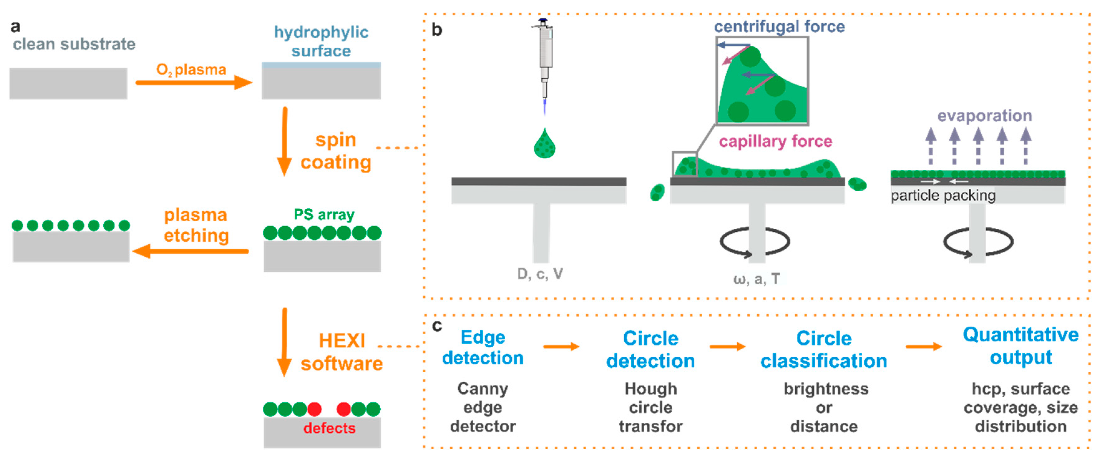
3.1. Self-Assembled Template Preparation by Spin Coating

3.1.1. Substrate Surface Properties

Before template preparation, some requirements had to be completed to cover the entire surface of the substrate evenly. First, the substrate must be well wetted by the solution. However, the cleaned substrates were highly hydrophobic (with a contact angle of ~80°). The substrates were pretreated with oxygen plasma, which made their surfaces hydrophilic (with a contact angle of less than 10°) [35]. The high wetting surface was a crucial requirement in order to obtain uniform monolayers. Chemical treatments, such as sonication in a hydrophilic solution (sulphuric acid, diodecyclo-sodiumsulfate solution, a mixture of ammonium hydroxide, hydrogen peroxide and ultrapure water, etc.) are also capable of changing the wettability of the substrates [36]. However, plasma treatment as a dry and nontoxic process is considered more environmentally friendly [37].

3.1.2. Colloidal Solution Properties

Before the spin coating process, the as-received colloidal solution (i.e., insoluble PS particles dispersed in a liquid) was sonicated in an ultrasonic bath, which ensured a homogeneous solution of spheres. Common polymer particles are generally hydrophobic. They tend to aggregate in an aqueous solution. For this reason, colloidal solutions often contain surfactant (such as anionic sodium dodecyl sulfate, nonionic sorbitan monolaurate, sodium bicarbonate, and potassium sulfate). Surface-active agents provide charge stabilization and reduce hydrophobicity and keep particles in a non-agglomerated state [38,39,40]. The solution that does not contain surfactant or salt has to be ultrasonicated for longer (~1 h) in order to isolate the particles.
The liquid substance was a crucial factor in the preparation of the colloidal solution [41]. A mixed solvent (water–alcohol mixture) was used. The alcohol solvent (such as methanol or ethanol) increased both the hydrophilicity of the surface and the evaporation rate of the solution. The alcoholic component evaporates relatively fast and results in a homogeneous coverage, whereas the other components (e.g., water) have slower evaporation rates, which give enough time for the particles to self-assemble before the substrate is entirely dry. A pure alcohol solution is inappropriate to create hcp monolayers because of its relatively high evaporation rate (the stacks of the spheres cannot be destroyed). The particles need time to achieve their lowest energy state before the surface is dried. The addition of surfactant (e.g., ethylene glycol, Triton X-100) to the solution is also commonly reported [27]. For our experiments, methanol was used with Triton X-100 in the volume ratio 400:1. Monolayers with few defects (high monolayer coverage, reduced voids, and multilayers) were obtained [6,27]. The surfactant improves the interparticle interaction, slows solvent evaporation, and enhances substrate wetting by decreasing the surface tension of the solvent mixture. Nontoxic nonionic polyoxyethylene (12) tridecyl ether can also be used as a surfactant. This nonionic surfactant has a covalently bonded oxygen-containing hydrophilic head group and a hydrophobic alkyl tail [27].
The correct dilution ratio of the colloidal solution with the alcoholic component was essential to achieve a uniform monolayer throughout the substrate (Figure 2). For our experiments, the colloidal PS (500 nm) solution was diluted by adding methanol-Triton X-100 in a 1:1 v/v ratio. If the mixture was too diluted, only partial coverage and noncompact islands were created, i.e., there was an inadequate amount of spheres in the solution to cover the whole substrate surface (Figure 2a,b). When a highly concentrated mixture was used, only multilayers were observed, without regard to the spin coating process variables. It should be noted that multilayers show not only hcp ordering but also metastable square close packing (Figure 2d).

3.1.3. Spin Coating Process Parameters

Next, the relevant spin coating process parameters (e.g., number of steps, speed, acceleration, time) were studied to obtain a uniform monolayer.
In general, a multistep procedure (two or three) was used [32]. The purpose of the first step (400 rpm for 10 s) was to evenly spread the solution on the surface, which increased the homogeneity of the final monolayer. It was essential to use an air bubble-free solution, since bubbles can cause defects in the monolayer. In the next step, the sample was accelerated to a higher rotation speed (1000–3000 rpm for 0.5–2 min, depending on the initial diameter of the PS). Centrifugal force, capillary force, and solvent evaporation arrange the spheres into well-ordered structures [28]. During this second step, the spheres must be able to slide on the substrate surface before the monolayer dries. When the second spinning speed was too high (i.e., high centrifugal force), the solvent evaporated very fast. Furthermore, the solution spun away from the center, leaving the central part less wet. The center is the starting point of the ordering. In such a case, the PS nanospheres formed monolayers, with partial coverage only, showing voids and many defects [3,42]. Similarly, if the second step was too short, the PS spheres would not have enough time to migrate on the substrate and achieve close packing. This resulted in loosely packed monolayers, where the interparticle capillary forces are weakened. During the third step, the centrifugal force needs to be high enough to remove any excess material (i.e., second and subsequent layers) from the substrate. If the rotation speed of this final step was too low, multilayers remained on the surface. If the rotation speed was too high, areas without spheres appeared in the monolayer. The proper process parameters (spin rate, time, acceleration, etc.) depend on the material and size of the spheres [26]. For example, spheres with a smaller diameter move faster, which indicates why a higher rotational speed must be applied.
The most frequently used polystyrene particles for NSL have a diameter ranging from 0.2 µm to 1 µm [9,27,34,43]. The theoretical model by Chandramohan et al. also showed that the ratios of PS spheres, water, methanol, and surfactant are the most crucial factors in achieving a densely packed and uniform monolayer. At lower speeds (<1000 rpm) inertia is negligible, and dry friction is less significant than gravitational force (independent of process parameters). The rotation speed and solid/liquid volume ratio were found to be the two key convoluted parameters of the spin coating process. Rotation speed defines the centrifugal force during the spin coating process. The amount of dispersion is crucial to the surface tension. These parameters are sufficient to describe the relative contribution of gravity, centrifugal, and capillary forces [9].

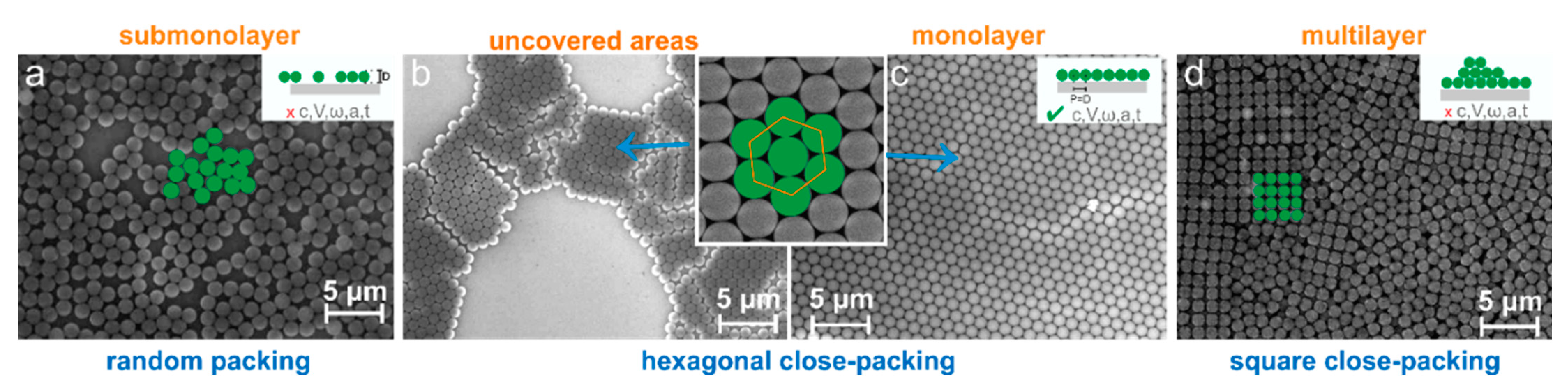
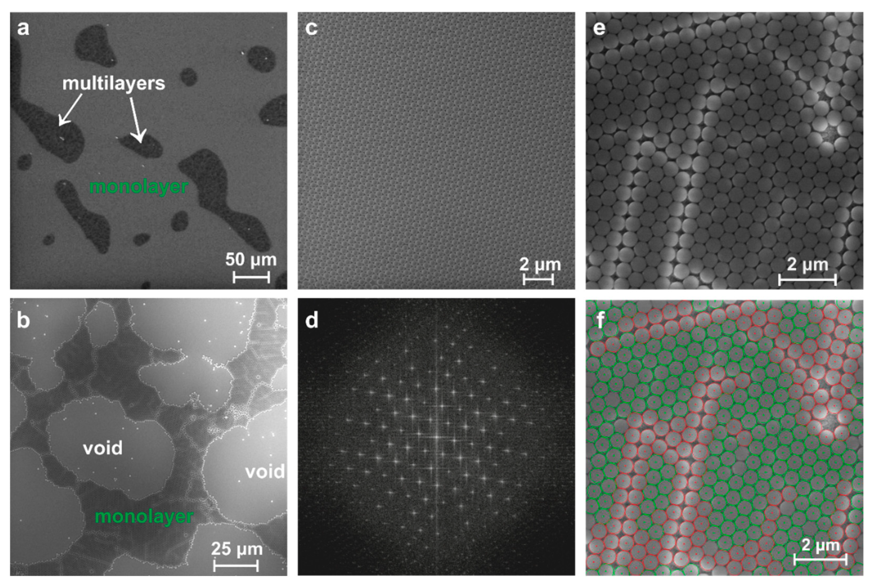
3.1.4. Self-Assembled Monolayer Characterisation

The first indication of the decent quality of a self-assembled monolayer is angle-dependent iridescent colour (for a better illustration, see Figure 3a—floating monolayer in a Petri dish and on Si substrate Figure 3b) generated from the Bragg diffraction of the visible light on the CC. After the spin coating process, the edges of the square (rotationally asymmetric) substrates were patchy because the corners create turbulence, resulting in poor coat quality (Figure 3c). The ‘coffee staining’ effect (the particles tend to form a ring-like pattern, which is macroscopic in size and visible to the naked eye), originating from the difference in the evaporation speeds across the droplet, was also observable as an undesirable pattern in some monolayers [24,28,44].
If eye observation indicated the uniform film quality, then a more detailed view of a monolayer of the PS nanospheres is characterized by scanning electron microscopy. SEM images were taken on each sample at various locations (e.g., center, edges).

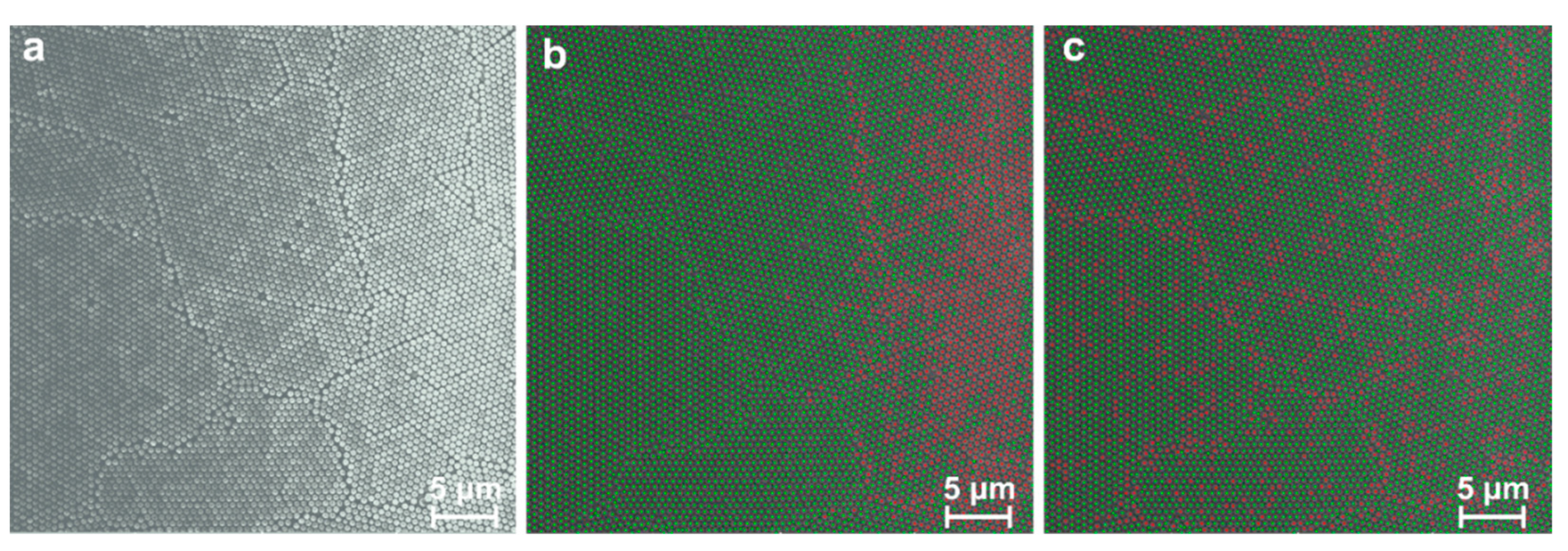
3.1.5. Ordering and Defects

Uniform self-assembled nanosphere hcp monolayers with triangularly shaped mask openings were obtained over a large surface using optimized preparation parameters. A representative SEM image of a good quality monolayer of PS spheres on a large surface area is shown in Figure 2c and Figure 4. The weak point of the spin coating method is that, in addition to the desired compact hcp monolayers, voids (uncovered regions), randomly and locally ordered single monolayers and mixed multilayers (e.g., hcp and square close-packed bilayers) can also occur on the same substrate (Figure 4). Figure 4e,f illustrate typical and most frequently occurring defects in PS monolayers. The spin coated monolayer is not defect-free, the defect formation among the spheres is inevitable due to the self-assembly mechanism. Large area monolayers contained different kinds of arrangement defects, including dislocations, multilayers, voids, domain boundaries, or disordered regions [26,31].
There are several reasons for the formation of such defects. Consistent quality (uniformity in size, shape, composition, and surface properties) of spheres is an essential prerequisite to obtain large area monolayers. The quality of the self-assembled CCs is mainly determined by the size distribution of the spheres. Point defects are related to the varying diameters of the spheres. Defect precursors, i.e., spheres with sizes bigger or smaller than the mean diameter of the population (Figure 4e,f), disrupt the hcp symmetry and induce imperfections in the CC.
The quality of the self-assembled monolayer is often assessed by fast Fourier transformations (FT) [28]. The Fourier transform image with sharp peaks is often used to demonstrate the six-fold symmetry of the self-assembled monolayer (Figure 4d), but it cannot provide a single intuitive result value that would express the ordering quality of the hcp mask [40]. The defect-free area of the hcp domain is in the range of 10–200 µm2 (greatly limited for spheres with polydisperse or multimodal size distribution) [23]. However, these values are based only on a rough estimate [4,12].
For accurate sample evaluation (verification of order and symmetry), we developed the open source image analysis software HEXI (implemented in Python), which detects circles and distinguishes between hcp ordering and defect configurations (e.g., point defects, dislocations) [45]. In the first stage, the algorithm identifies circular structures in SEM images using the Canny edge detector and the Hough circle transform (Figure 1c). Next, the detected circles are classified as hexagonally ordered spheres or defects (see Figure 4f with differently coloured circles drawn in the image) [46].

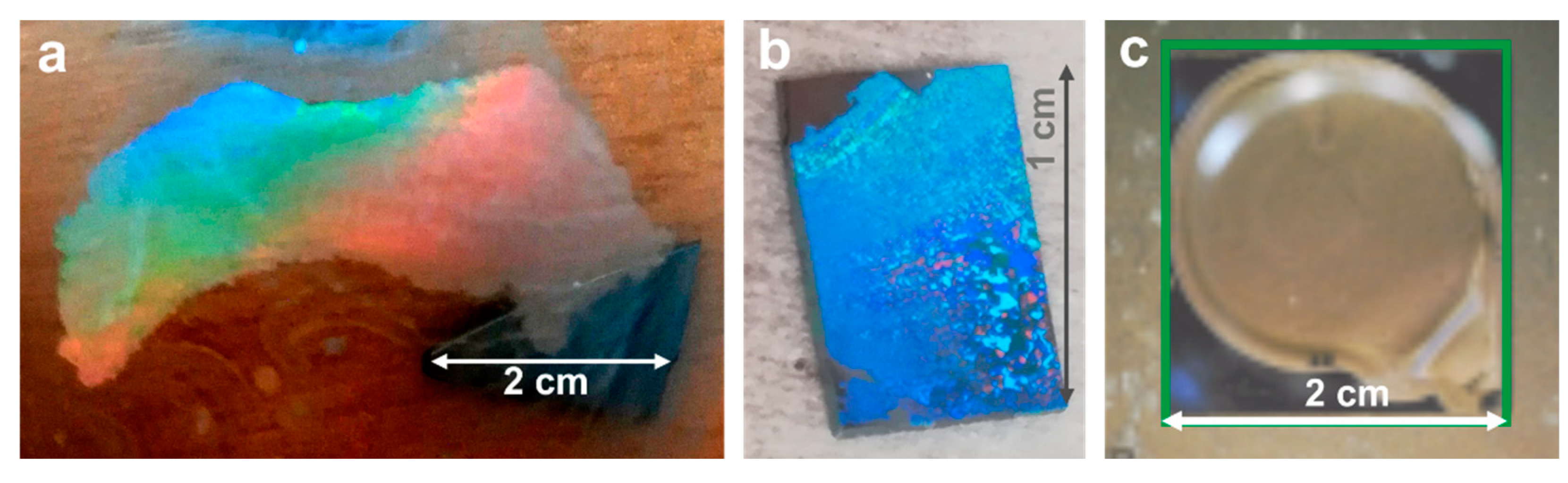
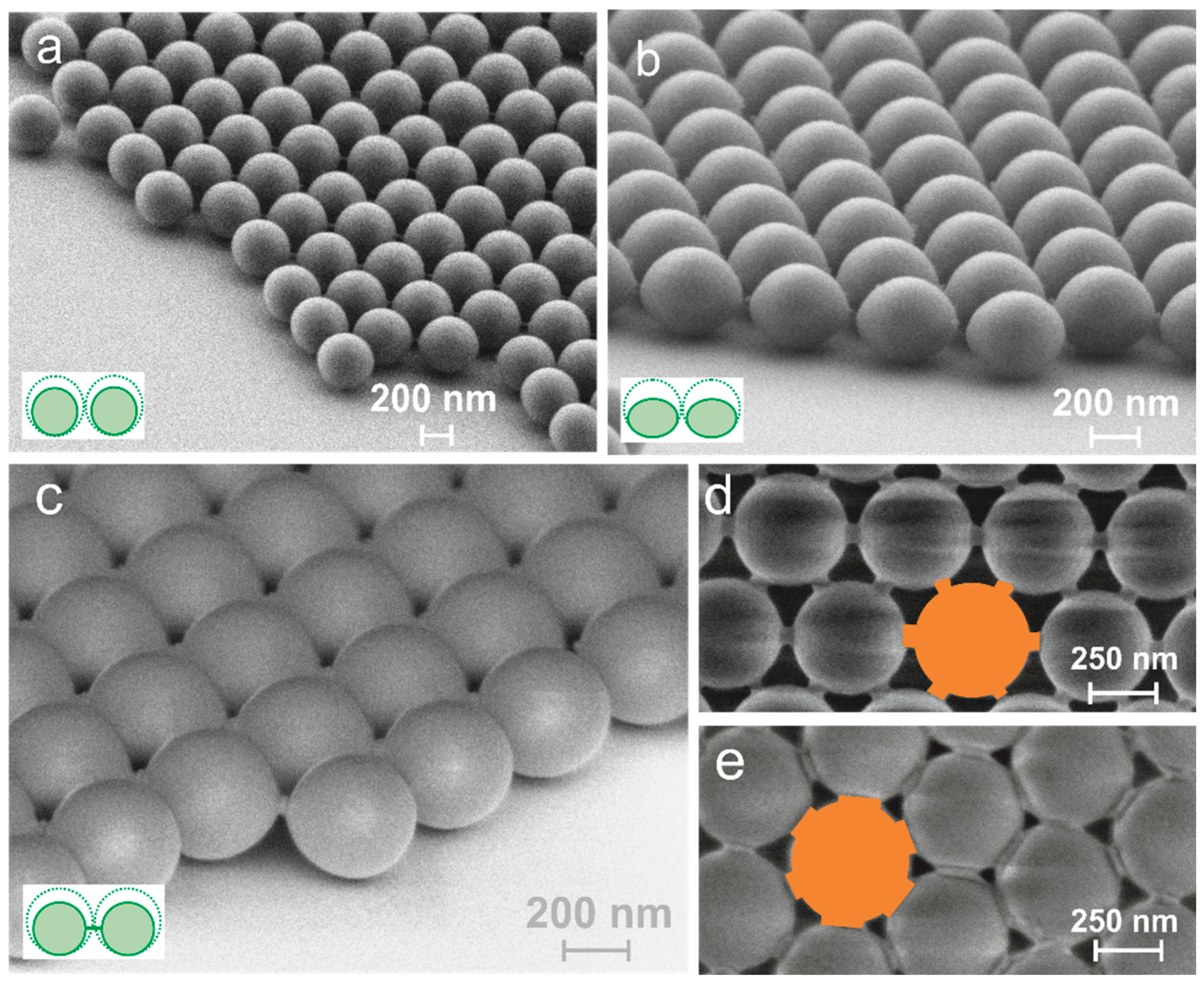
3.2. Template Modification by Plasma Etching

Arrays of non-close-packed spheres (i.e., equal spheres arranged in a periodic lattice and spaced out equally) were fabricated by plasma treatment of the initial close-packed arrays [30]. Plasma treatment adjusted the size of the individual spheres homogeneously throughout the sample. The original diameter of the spheres determined the periodicity (i.e., the distance between the sphere centres), which remained preserved after the plasma etching. The desired diameter and shape (degree of anisotropy) of the spheres, as well as the intersphere distance, were precisely adjusted via the choice of plasma system (CCP or LAP plasma) and etching process parameters (etching time, power, gas composition, total pressure, and self-bias voltage). Oxygen is the most commonly used working gas for the RIE of PS spheres [4]. During RIE, the hydrocarbon chains of the PS spheres are chemically decomposed into CO, CO2, and H2O and melted by the thermal energy of the plasma [34].

3.2.1. Reactive Ion Etching Using a Capacitively Coupled Plasma (CCP) System

Reactive ion etching in a capacitively coupled plasma system is an anisotropic process. The dependence of the diameter of the spheres on the etching time showed a nonlinear relationship [47]. Representative SEM images of PS spheres after etching in oxygen plasma are shown in Figure 5. The typical etching duration ranged from 30 s to 3 min (100 W, 12 Pa, 02:50 sccm for a PS sphere diameter of 500–1000 nm). The spheres remained in their original position. From angle view SEM images, it is clearly noticeable that the plasma etching reduced the diameter of the spheres; furthermore, it deformed the nanospheres into anisotropic particles. Their bottom profiles indicate that the etching process started from their top (ion bombarding occurred at the top part of the spheres). The contact area remained circular as long as the shape of the spheres was quasispherical (Figure 5b). The prolonged etching time resulted in surface roughening due to polymer degradation during oxygen-plasma etching associated with surface crosslinking [4,48].
Many applications require smooth sphere-like structures as templates that can be obtained by isotropic etching. Well-controlled circular pattern preparation is not an easy task in the CCP-RIE system because it is highly anisotropic and for longer etching times the sphere patterns collapse and irregular features (Figure 5c) are formed. The area between these irregular structures revealed a clean and flat surface (i.e., etching of the silicon substrate has not occurred). Further details on the effect of plasma process parameters can be found in our previous work [47].
In order to tune the morphology of the spheres, other gas mixtures or chemistry can be used, e.g., argon to induce chemical modifications in PS spheres, methanol to suppress cross-linking, HCl or hydrogen plasma to increase the chain scission effect compared to the cross-linking rate on the top of the surface, etc. [4]. Smooth PS nanosphere formation (Figure 5a) is achievable when (i) a short etching time is applied, or (ii) in cases where the original size of the PS nanospheres needs to be reduced only by a small value. To minimize surface roughening, Ar or CF4 can be added to the working gas [47]. The degree of anisotropy and surface roughening also depend on the temperature and the plasma system [48]. In general, to obtain smoother surfaces, lower temperatures (≤ambient temperature) or an inductively coupled plasma system have to be applied [4,19,49]. Etching in a plasma reactor equipped with a cooling system offers more isotropic etching and finer diameter and shape control due to lower etching rates [34,47,48,50]. Temperature is an uncontrollable parameter in our CCP-RIE device. The disruptive effect of the high energy ion bombardment can be reduced by decreasing the absolute value of the self-bias voltage. However, it cannot be controlled independently (because it is a function of RF power, pressure, and gas composition); therefore, the LAP plasma system was used for the optimal treatment of the PS spheres.

3.2.2. Etching in the LAP Plasma System

Our LAP plasma system combines both RF and MW plasmas, which allows independent control of the self-bias voltage on other operating parameters. MW plasma is responsible for enhancing the ion density (i.e., ion reservoir), while RF plasma accelerates the ions and electrons toward the sample. Thereby, well-controllable plasma treatment at voltage can be achieved, which determines the extent of surface bombardment. Furthermore, the heat flow is minimized because the substrate is located far from the plasma source. Consequently, the etching process is less aggressive (i.e., the surface smoothness of the PS spheres is preserved).
Figure 6 shows representative SEM images of PS spheres after etching in oxygen plasma in a LAP plasma system. These tilted SEM images reveal that various etching conditions resulted in various shapes, e.g., spherical, ellipsoidal, and ball-and-stick structures. The evolution of the shape depends mainly on the etching time. After periods of longer etching, the aspect ratio (diameter/height) increased, which turned the spheres into ellipsoidal particles. In Figure 6c,d the sphere-shaped structures are connected to each other with thin necks creating a net. In this case, the plasma etches the spheres gently, and their contacts are slowly converted to necks. These necks gradually thin out over time until they break and disappear at a critical spacing [47].
It can be concluded that the LAP system offers finer control over the diameter and shape of the nanospheres than the CCP-RIE system. First, the reduction in diameter of PS nanospheres is isotropic without surface roughening. Second, it can be applied even to smaller nanospheres (<500 nm) because a lower etching rate can be set in the LAP system. Both plasma devices allow processing of many samples at the same time because they have a large processing area (315 cm2 circle area and 600 cm2 rectangle area, for the CCP-RIE and LAP, respectively).
Net-like structures were also observed after thermal annealing (Figure 6e). During heating, the PS spheres fuse with each other and the point contacts between the particles are converted to area contacts due to melting of the soft PS polymer [51]. It should be noted that thermal treatment (in the case of PS close to the glass transition temperature of 100 °C; 5–10 s) also mechanically improves adhesion between the spheres and the substrate material [36,43]. However, the size of thermally formed neck-like connections often reveals larger sizes and limited controllability in comparison with PS treated in the LAP system.

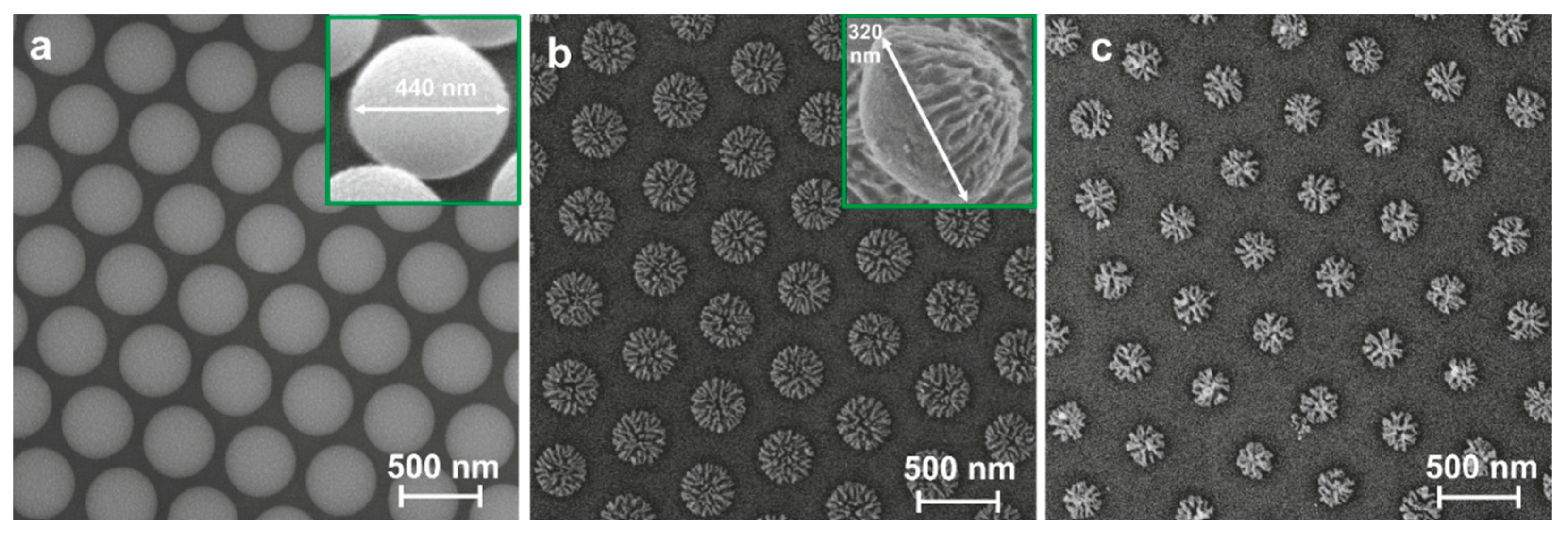
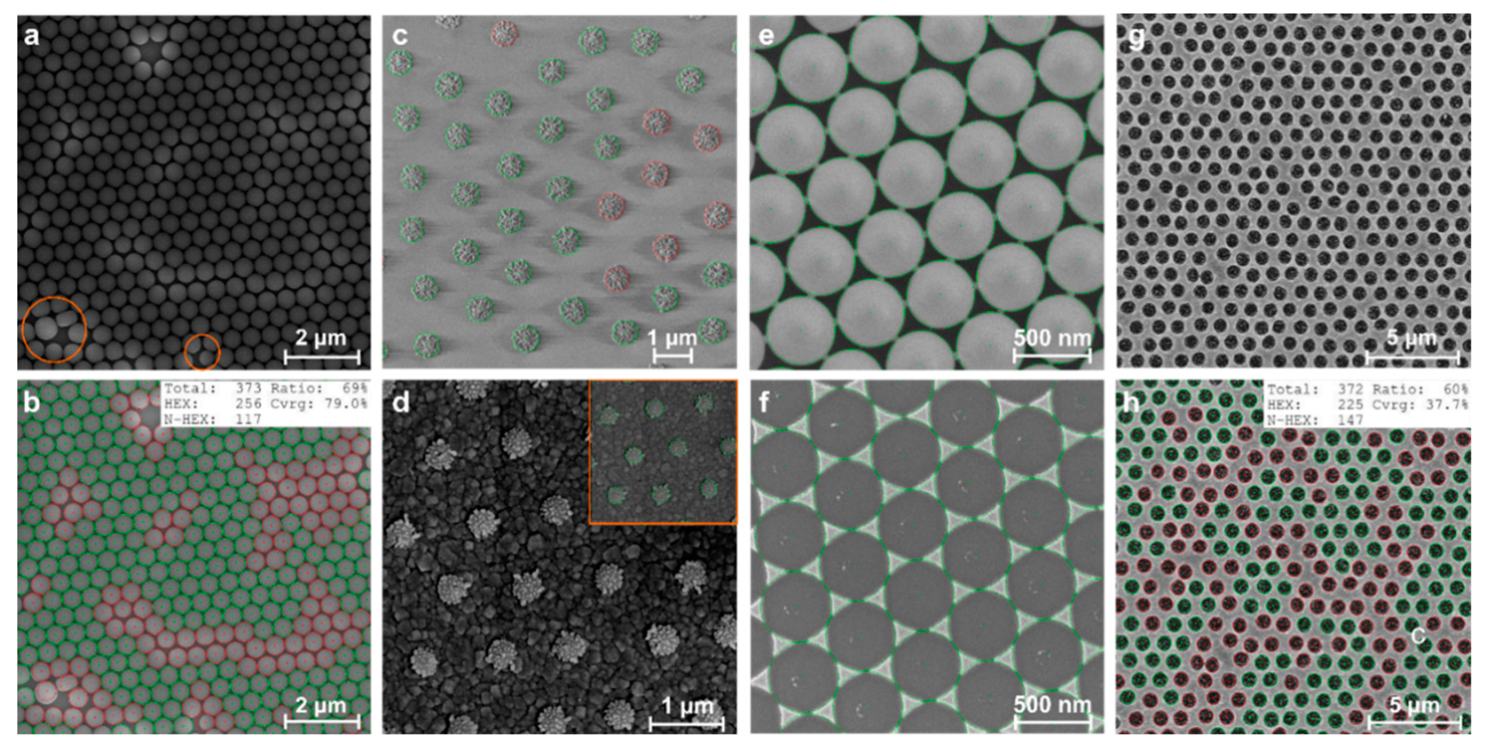
3.3. Applications and Symmetry Verification

Nanosphere lithography is an accessible and convenient approach to developing nanostructure arrays (e.g., tips, wires, cones, pillars, bowls, voids, holes, rings, etc.). In recent years, such types of structures have elicited much interest due to their alterable and definable characteristics (feature size, shape, periodicity, and material) [3,16,25,34]. Numerical modeling allows the determination of the appropriate dimensions of nanostructures for the targeted design and application [52]. The ordering of the arrays can vary from well-ordered to irregular. NSL can be embedded into many applications. Surfaces that mimic the morphologies and functionalities of natural materials (e.g., lotus leaves, the eye of a moth, wings of cicadas, shark skin, gecko feet, tree frog pads, bird and butterfly wings, peacock feathers) inspire researchers to create surfaces with specific properties (superhydrophobicity, self-cleaning, and antireflective properties) [2]. Optics, photonics, plasmonics, metamaterials, and sensorics seem to be the most promising fields of applications [16,19,53,54,55].
Polystyrene and silica spheres with a diameter of up to 2 µm are by far the most used beads because they can be easily synthetized monodispersed, deposited by spin-coating, and etched homogeneously [6]. Polystyrene is a popular polymer because of its unique properties, e.g., low cost and good processability (self-assembly, etching, lift-off, etc.), low water absorbability, and rigidity. The major benefit of the silica spheres is their higher heat resistance. They can be processed (i.e., by plasma etching) at a much higher temperature than polymer ones. Silica spheres can be used as mask material to create voids in thin films (e.g., diamond thin films) because they could withstand aggressive plasma deposition conditions. However, their removal is more difficult. Silica spheres can be dissolved in hydrofluoric acid [56].
Noble metal arrays of nanostructures have attracted a lot of attention for plasmonics and photonics due to their enhanced light-matter interaction in the vicinity of the nanostructures [57]. After the template preparation, the metal layer (e.g., gold, silver, platinum, palladium) can be evaporated over the spheres (Figure 7). These structures ‘metal film over nanosphere’ (the spheres represent an integral part of the final structure) have attracted great attention as surface-enhanced Raman spectroscopy (SERS) substrates [4,33]. In its simplest form, NSL results in triangular and spot structures using a three-step procedure: spin coating, thermal evaporation (unmodified monolayer and bilayer coated with a thin gold layer), and lift-off of the spheres (Figure 7f). The evaporated metal fills the gaps between the spheres. The desired nanostructures are achieved by removing the PS template by dissolution of PS in tetrahydrofuran, dichloromethane, or toluene by mild sonication [43,56,58]. Strong or long ultrasonication can cause damage to fragile samples (e.g., peeling off). Alternatively, it is possible to use standard adhesive tape to remove the sacrificial mask from the substrate. More complicated structures, e.g., rings, and crescents, can be achieved using a rotating evaporation angle [4,20].
Enhanced photoemission was achieved from laser-excited plasmonic nano-objects in periodic arrays (gold coated non-closed packed PS spheres, Figure 5b). Such an ordered array permitted the laser to excite a surface plasmon and drastically modified the emission of the gold sample (the yield of the electron current emitted was enhanced by a factor ~50) in comparison with a single crystal gold target [59].
Plasmonic nanoantenna arrays can be created by combining the self-assembly of PS nanospheres, reactive ion etching, and metal sputter coating [60]. Gold “nanocorals” (i.e., non-close-packed anisotropic structures) were created by gold sputtering on an array composed of structures shown in Figure 8b. Long-necked ball-and-stick structures (Figure 6c,d) were used as a template for gold sputtering to obtain a hexagonal array of gold bow-tie nanoantennas with controllable gap sizes. After the removal of the spheres, a planar triangle nanoantenna array was obtained that served as SERS-active substrates for ρ-aminothiophenol [60].
Our previous work has demonstrated the successful use of NSL for structuring polycrystalline diamond films of various surface roughnesses (microcrystalline and nanocrystalline) [56]. Diamond columns were created on pre-patterned surfaces (plasma etched PS spheres with an initial diameter of 250–940 nm) by selected area chemical vapour deposition (bottom-up approach) [61]. Hillock-like structures were created using a four-step top-down approach: nano-and microcrystalline diamond deposition, template preparation (PS spheres with an initial diameter of 1.5 µm), and plasma etching of PS spheres and diamond films using different plasma chemistries [62]. Unordered pores were obtained using SiO2 (with a diameter of 500 nm) in polycrystalline diamond films [56]. Photonic crystal slab, i.e., hexagonal air hole lattice (leaky mode in the near-infrared wavelength region at 1.31 μm) were fabricated on a quartz substrate using double masking PS monolayer and Au film (top-down approach) [52].
In the case of top-down strategies, new technological challenges occurred due to the different surface roughness of the diamond films, and it was crucial to apply the appropriate sphere size according to the initial roughness. It was found that the size of the crystallites of the diamond films had to be significantly smaller than the diameter of the PS spheres. The deposited diamond film had to be smooth enough (i.e., with a root mean square surface roughness < 20 nm) to be coated by a PS monolayer (500–1000 nm). In addition, the crystallites had to be homogeneous in size to avoid additional defect formation. For a more detailed description, see Refs. [52,56,63].

Quality Control of Circular Nanostructures with Hexagonal Symmetry

The permissible degree of disorder of the CCs depends on the application area [64]. Well-packed colloidal crystal (e.g., high degree of ordering, and minimal variation in the lattice constant) is essential to fabricate a photonic crystal. Contrarily, a certain degree of defects is still acceptable for sensing, photovoltaics, or photonic glass [3,15,19,65]. Defect inspection in the region of interest is essential to avoid jeopardizing the whole manufacturing process.
Figure 7 demonstrate the performance of the HEXI software under different circumstances. The advantage of the algorithm is that three different methods can be applied for defect classification based on the requirements of the image: variance in brightness (global or adaptive) and distance. Defect formation disrupts the ordering of the monolayer, and the distance between the sphere centres is no longer equal to the initial size of the spheres. In hcp monolayers, defects also show up as bright spots (see brightness deviations in Figure 4b,e). The increased brightness in the SEM images is a result of the edge effect because more secondary electrons are emitted on edges (gaps) than on densely packed areas. The simplest way to detect defects in hcp arrays is to use the global brightness classifier, because any visible brightness deviation in the SEM image is a clear indicator of a defect. The adaptive brightness-based classifier has to be applied to unevenly lit areas (common for large area images; see Figure 8—bright/dark areas independently of the defect locations) in order to balance the non-uniform illumination, which can be a problem in SEM imaging. In this case, the brightness threshold value varies depending on the average brightness of the local area (i.e., the threshold values are dynamically calculated for smaller areas of the image). The brightness classification method cannot be applied to non-closed packed arrays of spheres (e.g., plasma etched arrays, round holes after the lift-off process) because their uniform morphology (gap-sphere distribution) results in a uniform edge effect. For these samples, distance-based classification can be applied (Figure 7c,d,g,h). This classifier counts the number of nearest neighbours to each circle within a certain distance range. If there are <6 neighbouring circles (hcp symmetry) found within the specified threshold, a defect is identified in the SEM image. For nanostructures with poorly defined edges (Figure 7c), the image preprocessing (blurring) step must be applied for accurate edge detection.
It should be noted that HEXI can be successfully utilized for various types of circular nanostructures with hcp symmetry independently of the preparation method. Furthermore, it can be applied to images obtained by other types of microscopes (e.g., optical, atomic force microscope). In addition to the visual output (red/green circles), quantitative data can be generated (total and defective sphere count, surface coverage) even over large areas. Calculation of the radial distribution function (or pair correlation function) g(r) is another useful tool for quantifying the packing and ordering of hcp monolayers. It counts all spheres and then determines how many particles fall within an annular space. The normalized spectrum provides statistical information about the local sphere density relative to the average sphere density with respect to a reference sphere [66]. The histogram of the sphere size distribution can also be plotted. A graphical representation of the size distribution is useful for verifying the monodispersity of the spheres (purchased products or laboratory synthesized spheres). The histogram can also confirm that the plasma etching process occurred homogeneously across the entire surface area of the samples.
Image analysis-based characterisation of microscopy images allows comparison of the effectiveness of various nanostructuring methods. The outputs of the HEXI software can be used to improve existing manufacturing protocols (e.g., optimization of the spin-coating process, controlling and finetuning the etching process, verification of the repeatability of various steps, and better understanding of the self-assembly phenomena). Furthermore, the algorithm is designed to be extensible for other applications (e.g., nanostructures with different symmetry, and particles of non-spherical shape).

4. Conclusions

In this paper, a conceptual overview of nanosphere lithography is provided. For our experiments, spin coating was used to create large area monolayers of polystyrene spheres (with diameters lower than 1.5 µm) on Si or quartz substrates. The monodispersity of the nanospheres was a key factor in achieving a high-quality template with hexagonal symmetry. The template modification was achieved by reactive plasma etching, which allowed accurate, reproducible, and flexible size reduction of the PS spheres. The degree of anisotropy and surface roughening depended on the plasma device. After anisotropic etching in the CCP-RIE system, the PS particles were transferred into ellipsoidal structures, and surface roughening was also noticeable. Finer control of the spheres, i.e., nearly isotropic etching and low surface roughening, was observed in a linear antenna plasma system. NSL was also adapted to polycrystalline diamond films with various levels of surface roughness.
The major drawback of NSL is that the assembly process causes unavoidable defects. Accurate template quality control is essential to reliably produce periodic nanostructures with tailored characteristics and low defect density [26]. We developed a rapid and user-friendly image analysis tool for detecting structural defects in periodic circular nanostructures with hexagonal symmetry. We utilized the algorithm to evaluate spin coated hcp monolayers of polystyrene spheres, arrays of plasma etched nanospheres, holes, unevenly lit SEM images, and large areas.
We experimentally demonstrated that NSL is a powerful, inexpensive, and relatively fast alternative lithographic technique for creating a large variety of ordered arrays in a controlled fashion. This fabrication approach is capable of fabricating a broad variety of periodic structures (different shapes, periodicity, material, etc.). Although NSL is not comparable in flexibility, accuracy and resolution with common types of lithographic techniques, it wins out, however, in simplicity, price and fast processing, especially over larger surface areas (several cm2). It does not require the time-consuming and costly step of making a template with other lithography techniques. Instead of these, it uses self-assembled monolayers as templates and various nanostructuring methods. Throughout this overview, we summarized the specific advantages and limitations associated with the manufacturing processes.

Author Contributions

Conceptualization, M.D.; data curation, M.D.; software, M.D.; writing—original draft preparation, M.D.; writing—review and editing, A.K.; supervision, A.K. All authors have read and agreed to the published version of the manuscript.

Funding

This work used the large research infrastructure Czech NanoLab supported by the LM2018110 project. This work was supported by the Technical University in Prague, project No. SGS21/092/OHK1/2T/11.

Institutional Review Board Statement

Not applicable.

Data Availability Statement

The used software HEXI is available on gitHUb [45].

Acknowledgments

We acknowledge Rajisa Jackivová for SEM measurements and Andor Pathó for participation in software development.

Conflicts of Interest

The authors declare no conflict of interest.

References

  1. Varga, M.; Potocký, Š.; Domonkos, M.; Ižák, T.; Babčenko, O.; Kromka, A. Great variety of man-made porous diamond structures: Pulsed microwave cold plasma system with a linear antenna arrangement. ACS Omega 2019, 4, 8441–8450. [Google Scholar] [CrossRef] [PubMed] [Green Version]
  2. Bhushan, B.; Jung, Y.C. Natural and biomimetic artificial surfaces for superhydrophobicity, self-cleaning, low adhesion, and drag reduction. Prog. Mater. Sci. 2011, 56, 1–108. [Google Scholar] [CrossRef] [Green Version]
  3. Purwidyantri, A.; Tian, Y.-C.; Saputra, G.M.A.; Prabowo, B.A.; Liu, H.-L.; Yang, C.-M.; Lai, C.-S. Gold nanoframe array electrode for straightforward detection of hydrogen peroxide. Chemosensors 2021, 9, 37. [Google Scholar] [CrossRef]
  4. Lotito, V.; Zambelli, T. Playing with sizes and shapes of colloidal particles via dry etching methods. Adv. Colloid Interface Sci. 2021, 299, 102538. [Google Scholar] [CrossRef] [PubMed]
  5. Vakalopoulou, E.; Rath, T.; Warchomicka, F.G.; Carraro, F.; Falcaro, P.; Amenitsch, H.; Trimmel, G. Honeycomb-structured copper indium sulfide thin films obtained via a nanosphere colloidal lithography method. Mater. Adv. 2022, 3, 2884–2895. [Google Scholar] [CrossRef]
  6. Oliveira, R.D.; Mouquinho, A.; Centeno, P.; Alexandre, M.; Haque, S.; Martins, R.; Fortunato, E.; Águas, H.; Mendes, M.J. Colloidal lithography for photovoltaics: An attractive route for light management. Nanomaterials 2021, 11, 1665. [Google Scholar] [CrossRef]
  7. Ye, X.; Qi, L. Two-dimensionally patterned nanostructures based on monolayer colloidal crystals: Controllable fabrication, assembly, and applications. Nano Today 2011, 6, 608–631. [Google Scholar] [CrossRef]
  8. van Dommelen, R.; Fanzio, P.; Sasso, L. Surface self-assembly of colloidal crystals for micro- and nano-patterning. Adv. Colloid Interface Sci. 2017, 251, 97–114. [Google Scholar] [CrossRef]
  9. Chandramohan, A.; Sibirev, N.V.; Dubrovskii, V.G.; Petty, M.C.; Gallant, A.J.; Zeze, D.A. Model for large-area monolayer coverage of polystyrene nanospheres by spin coating. Sci. Rep. 2017, 7, 40888. [Google Scholar] [CrossRef] [Green Version]
  10. Kralchevsky, P.A.; Denkov, N.D. Capillary forces and structuring in layers of colloid particles. Curr. Opin. Colloid Interface Sci. 2001, 6, 383–401. [Google Scholar] [CrossRef]
  11. Israelachvili, J.N. Intermolecular and Surface Forces; Academic Press: Burlington, MA, USA, 2011; ISBN 978-0-12-375182-9. [Google Scholar]
  12. Correia, E.L.; Brown, N.; Razavi, S. Janus particles at fluid interfaces: Stability and interfacial rheology. Nanomaterials 2021, 11, 374. [Google Scholar] [CrossRef] [PubMed]
  13. Liu, G.; Cai, W. Morphological and structural control of organic monolayer colloidal crystal based on plasma etching and its application in fabrication of ordered gold nanostructured arrays. Crystals 2016, 6, 126. [Google Scholar] [CrossRef] [Green Version]
  14. Zhang, J.; Li, L.; Liu, D.; Zhang, J.; Hao, Y.; Zhang, W. Multi-layer and open three-dimensionally ordered macroporous TiO2–ZrO2 composite: Diversified design and the comparison of multiple mode photocatalytic performance. Mater. Des. 2015, 86, 818–828. [Google Scholar] [CrossRef]
  15. Döhler, D.; Triana, A.; Büttner, P.; Scheler, F.; Goerlitzer, E.S.A.; Harrer, J.; Vasileva, A.; Metwalli, E.; Gruber, W.; Unruh, T.; et al. A self-ordered nanostructured transparent electrode of high structural quality and corresponding functional performance. Small 2021, 17, 2100487. [Google Scholar] [CrossRef] [PubMed]
  16. Lospinoso, D.; Colombelli, A.; Lomascolo, M.; Rella, R.; Manera, M.G. Self-assembled metal nanohole arrays with tunable plasmonic properties for SERS single-molecule detection. Nanomaterials 2022, 12, 380. [Google Scholar] [CrossRef]
  17. Dvoretckaia, L.; Gridchin, V.; Mozharov, A.; Maksimova, A.; Dragunova, A.; Melnichenko, I.; Mitin, D.; Vinogradov, A.; Mukhin, I.; Cirlin, G. Light-emitting diodes based on InGaN/GaN nanowires on microsphere-lithography-patterned Si substrates. Nanomaterials 2022, 12, 1993. [Google Scholar] [CrossRef] [PubMed]
  18. Colombelli, A.; Lospinoso, D.; Rella, R.; Manera, M.G. Shape Modulation of Plasmonic Nanostructures by Unconventional Lithographic Technique. Nanomaterials 2022, 12, 547. [Google Scholar] [CrossRef] [PubMed]
  19. Pander, A.; Onishi, T.; Hatta, A.; Furuta, H. Fabrication of self-assembling carbon nanotube forest fishnet metamaterials. Nanomaterials 2022, 12, 464. [Google Scholar] [CrossRef]
  20. Wang, Y.; Zhang, M.; Lai, Y.; Chi, L. Advanced colloidal lithography: From patterning to applications. Nano Today 2018, 22, 36–61. [Google Scholar] [CrossRef]
  21. Lotito, V.; Zambelli, T. Approaches to self-assembly of colloidal monolayers: A guide for nanotechnologists. Adv. Colloid Interface Sci. 2017, 246, 217–274. [Google Scholar] [CrossRef]
  22. Tufail Chaudhary, K. Thin film deposition: Solution based approach. In Thin Films; Esther Ares, A., Ed.; IntechOpen: London, UK, 2021; ISBN 978-1-83881-986-6. [Google Scholar]
  23. Colson, P.; Henrist, C.; Cloots, R. Nanosphere lithography: A powerful method for the controlled manufacturing of nanomaterials. J. Nanomater. 2013, 2013, 19. [Google Scholar] [CrossRef] [Green Version]
  24. Kaliyaraj Selva Kumar, A.; Zhang, Y.; Li, D.; Compton, R.G. A mini-review: How reliable is the drop casting technique? Electrochem. Commun. 2020, 121, 106867. [Google Scholar] [CrossRef]
  25. Huang, Y.H.; Lin, H.C.; Cheng, S.L. Fabrication of vertically well-aligned NiSi2 nanoneedle arrays with enhanced field emission properties. J. Phys. Chem. Solids 2021, 150, 109892. [Google Scholar] [CrossRef]
  26. Lee, D.; Tang, Y.-L.; Liu, S.-J. Fast fabrication of nanostructured films using nanocolloid lithography and UV soft mold roller embossing: Effects of processing parameters. Polymers 2021, 13, 405. [Google Scholar] [CrossRef]
  27. Park, B.; Na, S.Y.; Bae, I.-G. Uniform two-dimensional crystals of polystyrene nanospheres fabricated by a surfactant-assisted spin-coating method with polyoxyethylene tridecyl ether. Sci. Rep. 2019, 9, 11453. [Google Scholar] [CrossRef] [Green Version]
  28. Toolan, D.T.W.; Fujii, S.; Ebbens, S.J.; Nakamura, Y.; Howse, J.R. On the mechanisms of colloidal self-assembly during spin-coating. Soft Matter 2014, 10, 8804–8812. [Google Scholar] [CrossRef]
  29. Domonkos, M.; Ižák, T.; Kromka, A.; Varga, M. Polymer-based nucleation for chemical vapour deposition of diamond. J. Appl. Polym. Sci. 2016, 133, 43688. [Google Scholar] [CrossRef]
  30. Cheon, S.-E.; Lee, H.; Choi, J.; Jeong, A.R.; Lee, T.S.; Jeong, D.S.; Lee, K.-S.; Lee, W.-S.; Kim, W.M.; Lee, H.; et al. Fabrication of parabolic Si nanostructures by nanosphere lithography and its application for solar cells. Sci. Rep. 2017, 7, 7336. [Google Scholar] [CrossRef]
  31. Ižák, T.; Domonkos, M.; Babchenko, O.; Varga, M.; Rezek, B.; Jurka, V.; Hruška, K.; Kromka, A. Technological aspects in fabrication of micro- and nano-sized carbon based features: Nanorods, periodical arrays and self-standing membranes. J. Electr. Eng. 2015, 66, 282–286. [Google Scholar] [CrossRef] [Green Version]
  32. Lei, P.-H.; Yang, P.-C.; Huang, P.-C. Investigation of Photonic-Crystal-Structured p-GaN Nanorods Fabricated by Polystyrene Nanosphere Lithography Method to Improve the Light Extraction Efficiency of InGaN/GaN Green Light-Emitting Diodes. Materials 2021, 14, 2200. [Google Scholar] [CrossRef]
  33. Quero, G.; Zito, G.; Managò, S.; Galeotti, F.; Pisco, M.; De Luca, A.; Cusano, A. Nanosphere lithography on fiber: Towards engineered lab-on-fiber SERS optrodes. Sensors 2018, 18, 680. [Google Scholar] [CrossRef] [PubMed] [Green Version]
  34. Chen, Y.; Shi, D.; Chen, Y.; Chen, X.; Gao, J.; Zhao, N.; Wong, C.-P. A facile, low-cost plasma etching method for achieving size controlled non-close-packed monolayer arrays of polystyrene nano-spheres. Nanomaterials 2019, 9, 605. [Google Scholar] [CrossRef] [PubMed] [Green Version]
  35. Domonkos, M.; Tichá, P. Wettability of SiO2 nanofibrous mats and their modification using cold atmospheric plasma treatment. Acta Phys. Pol. A 2021, 140, 181–185. [Google Scholar] [CrossRef]
  36. Li, W.; Wang, S.; He, S.; Hu, M.; Ge, P.; Wang, J.; Guo, Y. Controlled fabrication of Si nanowires with nanodots using nanosphere lithography. J. Nanosci. Nanotechnol. 2016, 16, 1537–1540. [Google Scholar] [CrossRef]
  37. Domonkos, M.; Tichá, P.; Trejbal, J.; Demo, P. Applications of cold atmospheric pressure plasma technology in medicine, agriculture and food industry. Appl. Sci. 2021, 11, 4809. [Google Scholar] [CrossRef]
  38. Jódar-Reyes, A.B.; Martín-Rodríguez, A.; Ortega-Vinuesa, J.L. Effect of the ionic surfactant concentration on the stabilization/destabilization of polystyrene colloidal particles. J. Colloid Interface Sci. 2006, 298, 248–257. [Google Scholar] [CrossRef]
  39. Shrestha, S.; Wang, B.; Dutta, P. Nanoparticle processing: Understanding and controlling aggregation. Adv. Colloid Interface Sci. 2020, 279, 102162. [Google Scholar] [CrossRef]
  40. Ye, X.; Huang, J.; Zeng, Y.; Sun, L.-X.; Geng, F.; Liu, H.-J.; Wang, F.-R.; Jiang, X.-D.; Wu, W.-D.; Zheng, W.-G. Monolayer colloidal crystals by modified air-water interface self-assembly approach. Nanomaterials 2017, 7, 291. [Google Scholar] [CrossRef] [Green Version]
  41. Wu, Y.; Xu, X.; Zhang, H.; Liu, L.; Li, J.; Yang, D. Improving self-assembly quality of colloidal crystal guided by statistical design of experiments. Chin. Phys. B 2017, 26, 038105. [Google Scholar] [CrossRef]
  42. Zhang, C.; Cvetanovic, S.; Pearce, J.M. Fabricating ordered 2-D nano-structured arrays using nanosphere lithography. MethodsX 2017, 4, 229–242. [Google Scholar] [CrossRef]
  43. Jamiolkowski, R.M.; Chen, K.Y.; Fiorenza, S.A.; Tate, A.M.; Pfeil, S.H.; Goldman, Y.E. Nanoaperture fabrication via colloidal lithography for single molecule fluorescence analysis. PLoS ONE 2019, 14, e0222964. [Google Scholar] [CrossRef] [PubMed] [Green Version]
  44. Marcel Sperling; Michael Gradzielski Droplets, evaporation and a superhydrophobic surface: Simple tools for guiding colloidal particles into complex materials. Gels 2017, 3, 15. [CrossRef] [PubMed] [Green Version]
  45. Available online: https://github.com/domonmar/HEXI (accessed on 10 December 2022).
  46. Domonkos, M.; Jackivová, R.; Pathó, A. Image analysis algorithm for the verification of hexagonal symmetry in spherical nanostructures. Microelectron. Eng. 2022, 251, 111635. [Google Scholar] [CrossRef]
  47. Domonkos, M.; Ižák, T.; Štolcová, L.; Proška, J.; Kromka, A. Controlled structuring of self-assembled polystyrene microsphere arrays by two different plasma systems. In Proceedings of the 5th International Conference NANOCON 2013 Conference Proceedings, Ostrava, Czech Republic, 16–18 October 2013. [Google Scholar]
  48. Darvill, D.; Iarossi, M.; Abraham Ekeroth, R.M.; Hubarevich, A.; Huang, J.-A.; De Angelis, F. Breaking the symmetry of nanosphere lithography with anisotropic plasma etching induced by temperature gradients. Nanoscale Adv. 2021, 3, 359–369. [Google Scholar] [CrossRef] [PubMed]
  49. Plettl, A.; Enderle, F.; Saitner, M.; Manzke, A.; Pfahler, C.; Wiedemann, S.; Ziemann, P. Non-close-packed crystals from self-assembled polystyrene spheres by isotropic plasma etching: Adding flexibility to colloid lithography. Adv. Funct. Mater. 2009, 19, 3279–3284. [Google Scholar] [CrossRef]
  50. Akinoglu, E.M.; Morfa, A.J.; Giersig, M. Understanding anisotropic plasma etching of two-dimensional polystyrene opals for advanced materials fabrication. Langmuir 2014, 30, 12354–12361. [Google Scholar] [CrossRef]
  51. Geng, C.; Zheng, L.; Yu, J.; Yan, Q.; Wei, T.; Wang, X.; Shen, D. Thermal annealing of colloidal monolayer at the air/water interface: A facile approach to transferrable colloidal masks with tunable interstice size for nanosphere lithography. J. Mater. Chem. 2012, 22, 22678. [Google Scholar] [CrossRef]
  52. Domonkos, M.; Varga, M.; Ondič, L.; Gajdošová, L.; Kromka, A. Microsphere lithography for scalable polycrystalline diamond-based near-infrared photonic crystals fabrication. Mater. Des. 2018, 139, 363–371. [Google Scholar] [CrossRef]
  53. Khan, P.; Brennan, G.; Lillis, J.; Tofail, S.A.M.; Liu, N.; Silien, C. Characterisation and manipulation of polarisation response in plasmonic and magneto-plasmonic nanostructures and metamaterials. Symmetry 2020, 12, 1365. [Google Scholar] [CrossRef]
  54. Barbillon, G.; Ivanov, A.; Sarychev, A.K. Applications of symmetry breaking in plasmonics. Symmetry 2020, 12, 896. [Google Scholar] [CrossRef]
  55. Šišoláková, I.; Petruš, O.; Shepa, J.; Farka, Z.; Oriňak, A.; Oriňaková, R. Colloidal lithography as a novel approach for the development of Ni-nanocavity insulin sensor. Sci. Rep. 2022, 12, 11020. [Google Scholar] [CrossRef] [PubMed]
  56. Domonkos, M.; Demo, P.; Kromka, A. Nanosphere lithography for structuring polycrystalline diamond films. Crystals 2020, 10, 118. [Google Scholar] [CrossRef] [Green Version]
  57. Pisco, M.; Galeotti, F.; Quero, G.; Grisci, G.; Micco, A.; Mercaldo, L.V.; Veneri, P.D.; Cutolo, A.; Cusano, A. Nanosphere lithography for optical fiber tip nanoprobes. Light Sci. Appl. 2017, 6, e16229. [Google Scholar] [CrossRef] [PubMed] [Green Version]
  58. Aiempanakit, M.; Jearnkulprasert, N.; Panyajirawut, P. Patterning of nanoparticle arrays by self-assembly lithography. Mater. Today Proc. 2017, 4, 6009–6014. [Google Scholar] [CrossRef]
  59. Fedorov, N.; Geoffroy, G.; Duchateau, G.; Štolcová, L.; Proška, J.; Novotný, F.; Domonkos, M.; Jouin, H.; Martin, P.; Raynaud, M. Enhanced photoemission from laser-excited plasmonic nano-objects in periodic arrays. J. Phys. Condens. Matter 2016, 28, 315301. [Google Scholar] [CrossRef]
  60. Stolcová, L.; Domonkos, M.; Izák, T.; Proska, J.; Procházka, M.; Kromka, A. Plasma treatment as a versatile technique for preparation of plasmonic nanoantenna arrays. In Proceedings of the Progress in Electromagnetics Research Symposium (PIERS) Proceedings, Stockholm, Sweden, 12–15 August 2013; pp. 426–430. [Google Scholar]
  61. Domonkos, M.; Izak, T.; Stolcova, L.; Proska, J.; Kromka, A. Fabrication of periodically ordered diamond nanostructures by microsphere lithography. Phys. Status Solidi B 2014, 251, 2587–2592. [Google Scholar] [CrossRef]
  62. Domonkos, M.; Ižák, T.; Štolcová, L.; Proška, J.; Demo, P.; Kromka, A. Structuring of diamond films using microsphere lithography. Acta Polytech. 2014, 54, 320–324. [Google Scholar] [CrossRef]
  63. Akinoglu, E.M.; Morfa, A.; Giersig, M. Nanosphere lithography-exploiting self-assembly on the nanoscale for sophisticated nanostructure fabrication. Turk. J. Phys. 2014, 38, 563–572. [Google Scholar] [CrossRef] [Green Version]
  64. Pisco, M.; Galeotti, F. Nano- and Micropatterning on Optical Fibers by Bottom-Up Approach: The Importance of Being Ordered. Appl. Sci. 2021, 11, 3254. [Google Scholar] [CrossRef]
  65. García, P.D.; Sapienza, R.; Blanco, á.; López, C. Photonic glass: A novel random material for light. Adv. Mater. 2007, 19, 2597–2602. [Google Scholar] [CrossRef]
  66. Van Hooghten, R.; Blair, V.E.; Vananroye, A.; Schofield, A.B.; Vermant, J.; Thijssen, J.H.J. Interfacial Rheology of Sterically Stabilized Colloids at Liquid Interfaces and Its Effect on the Stability of Pickering Emulsions. Langmuir 2017, 33, 4107–4118. [Google Scholar] [CrossRef] [PubMed]
Figure 1. (a) Overview of the main steps used during template preparation. (b) Schematic drawing of the main stages of the monolayer deposition by spin coating. (c) Key stages of the image analysis algorithm (HEXI software) used to verify the quality of the template.
Symmetry 14 02642 g001
Figure 2. Schematic illustration of submonolayer, monolayer, and multilayer coverage regions after the spin coating process.
Symmetry 14 02642 g002
Figure 3. Monolayer of PS nanospheres on the (a) water surface and (b) Si samples. Macroscopic image of PS spheres displaying rainbow iridescence. (c) spin coated monolayer on a square substrate with patchy edges.
Symmetry 14 02642 g003
Figure 4. (a,b) Low magnification SEM images of PS arrays predominantly coated by voids and multilayers. (c) Highly ordered monolayer with hcp ordering and (d) corresponding FT image. (e) Monolayer with typical defects and (f) defect evaluation using the HEXI software.
Symmetry 14 02642 g004
Figure 5. Representative images of non-close packed PS sphere arrays. The diameter of the spheres was reduced via oxygen plasma treatment using the CCP-RIE system (100 W, 12 Pa, 02:50 sccm, (a) 10 s, (b) 30 s and (c) 1 min).
Symmetry 14 02642 g005
Figure 6. Representative angle-view SEM images of non-close packed PS spheres with different shapes. (a) spherical (10 Pa, 600 W RF power, 10 V, 1 min), (b) ellipsoidal (3 min) and (c) ball-and-stick structures obtained after oxygen plasma etching in the LAP device (10 Pa, 1200 W (MW) + 600 W (RF), 10 V, 3 min). Top view SEM images of ball-and-stick structures (d) after plasma etching in the LAP plasma system and (e) after thermal treatment.
Symmetry 14 02642 g006
Figure 7. Representative SEM images evaluated using the HEXI software. (a) Raw and (b) evaluated (brightness-based classifier) hcp monolayer with typical defects (vacancy, dislocations); (c) plasma etched nanosphere array (distance-based classifier), (d) plasma etched nanosphere array over a polycrystalline diamond thin film, (e) ball-and-stick structures over a Si substrate, (f) defect free array of triangular nanostructures created using lift-off the PS sphere template, (g,h) holes in diamond thin film with high defect density.
Symmetry 14 02642 g007
Figure 8. (a) SEM image of a large area monolayer with uneven illumination (b) evaluated using global and (c) adaptive brightness classifier.
Symmetry 14 02642 g008
Publisher’s Note: MDPI stays neutral with regard to jurisdictional claims in published maps and institutional affiliations.

