
Soft-Switching Full-Bridge Converter with Multiple-Input Sources for DC Distribution Applications


Abstract
:1. Introduction
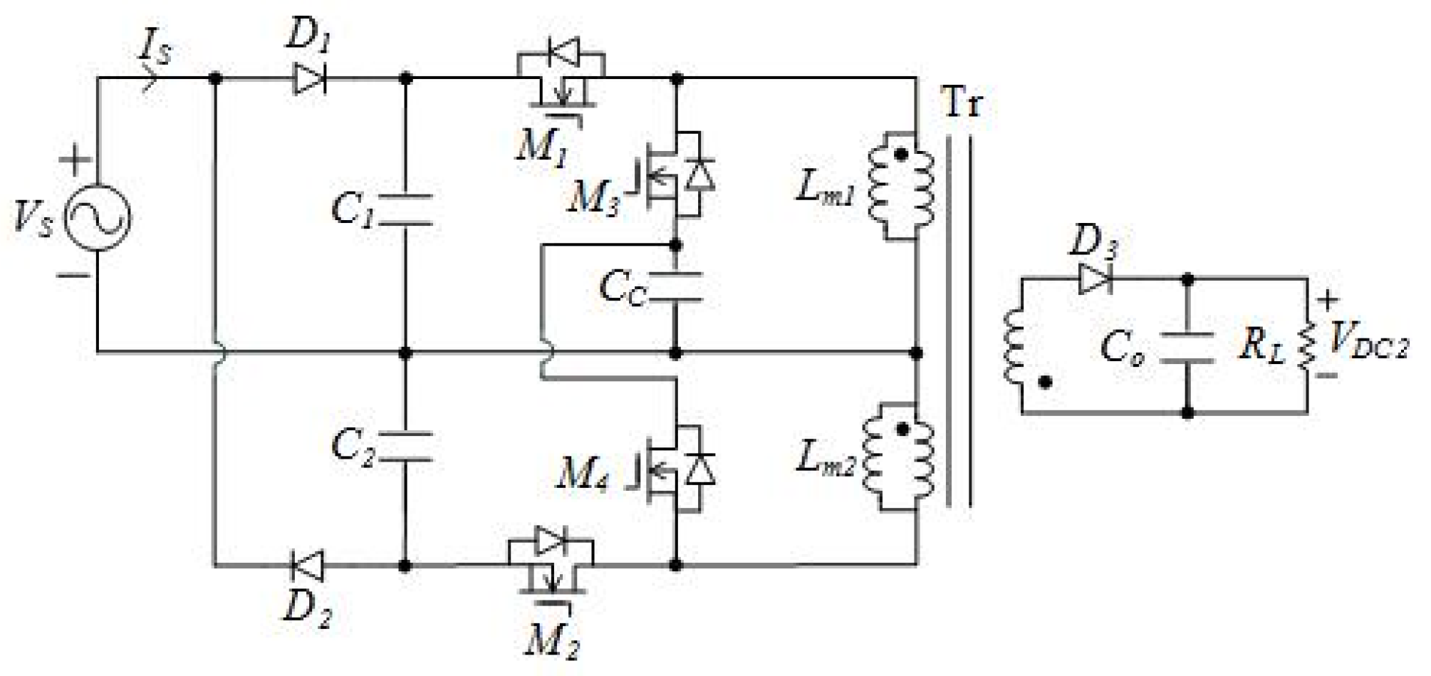
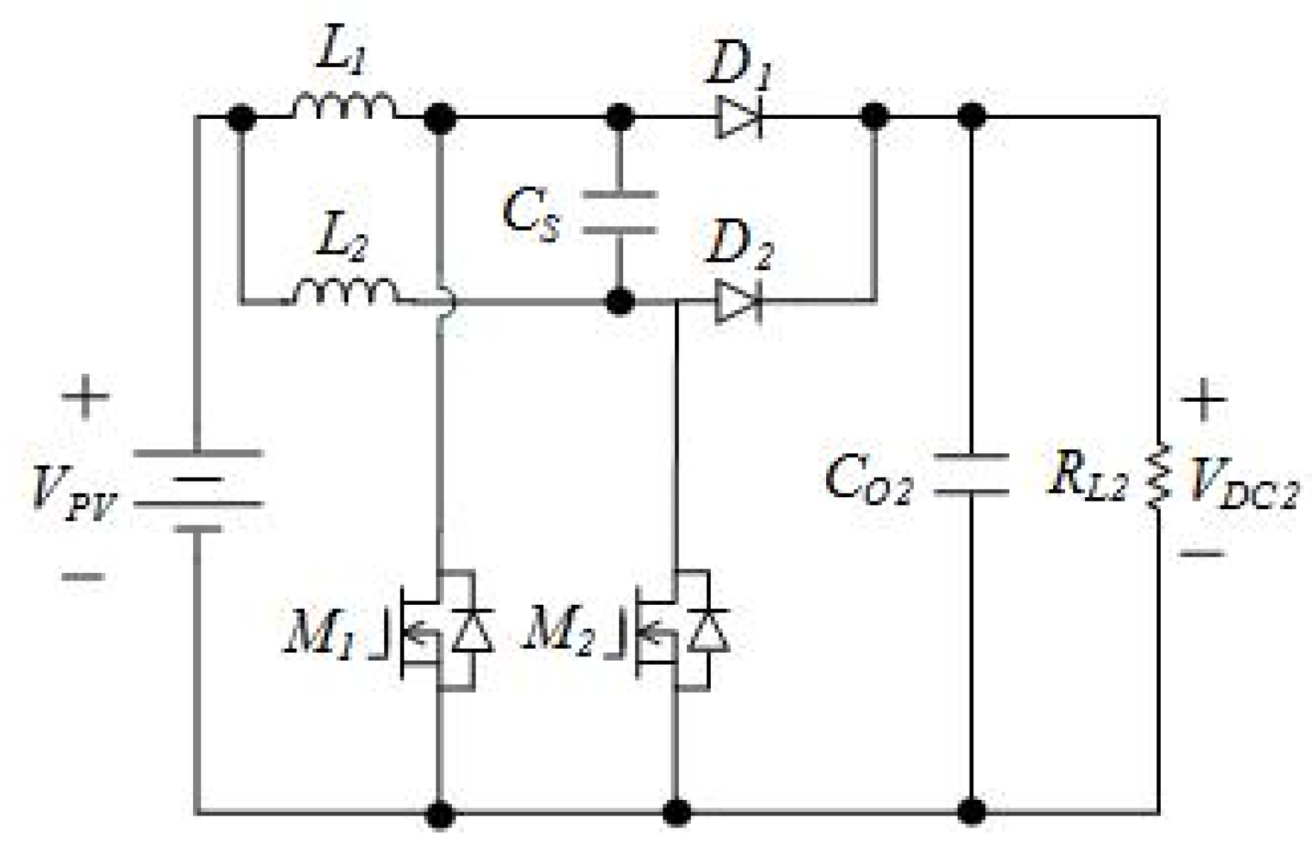
2. Related Work
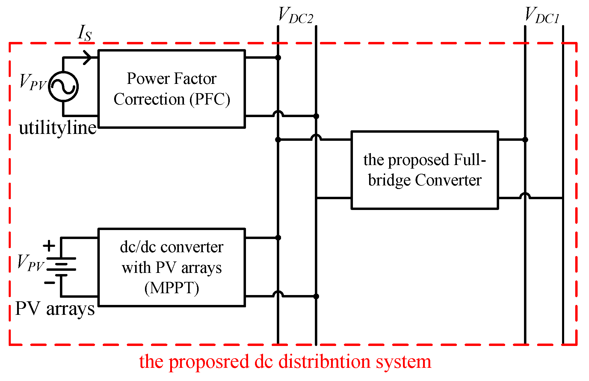
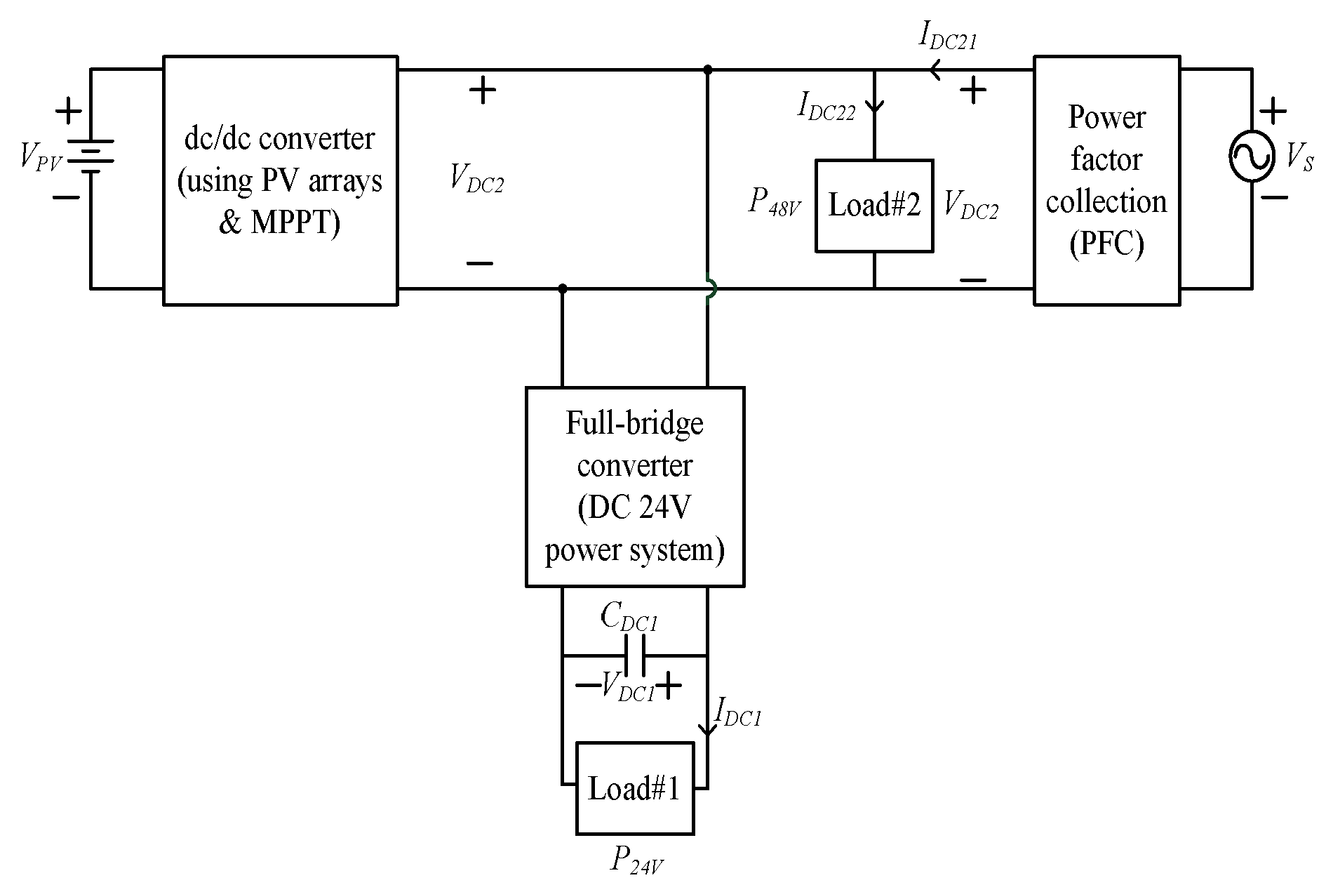
3. Topology and Operational Method of the Proposed DC Distribution Power
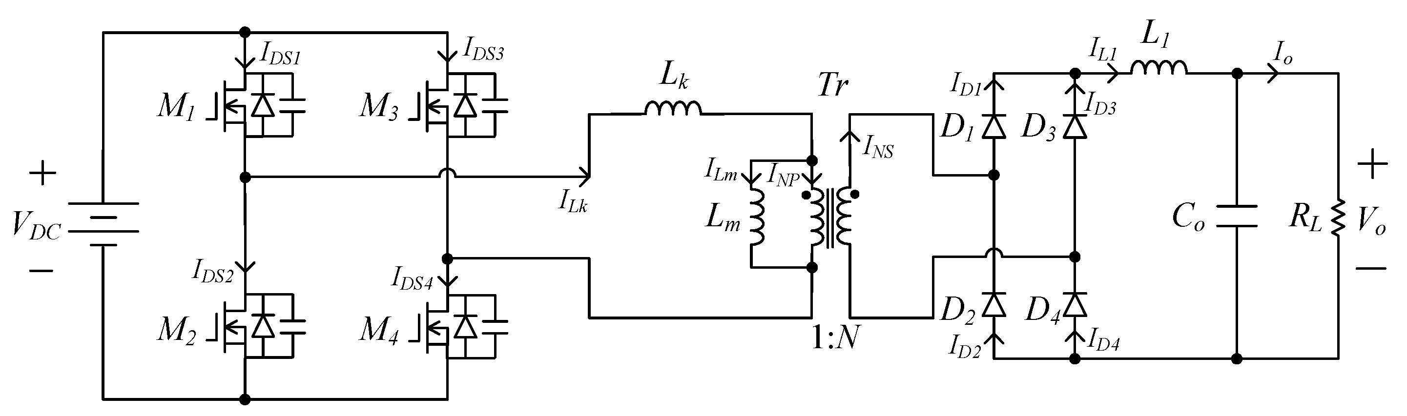
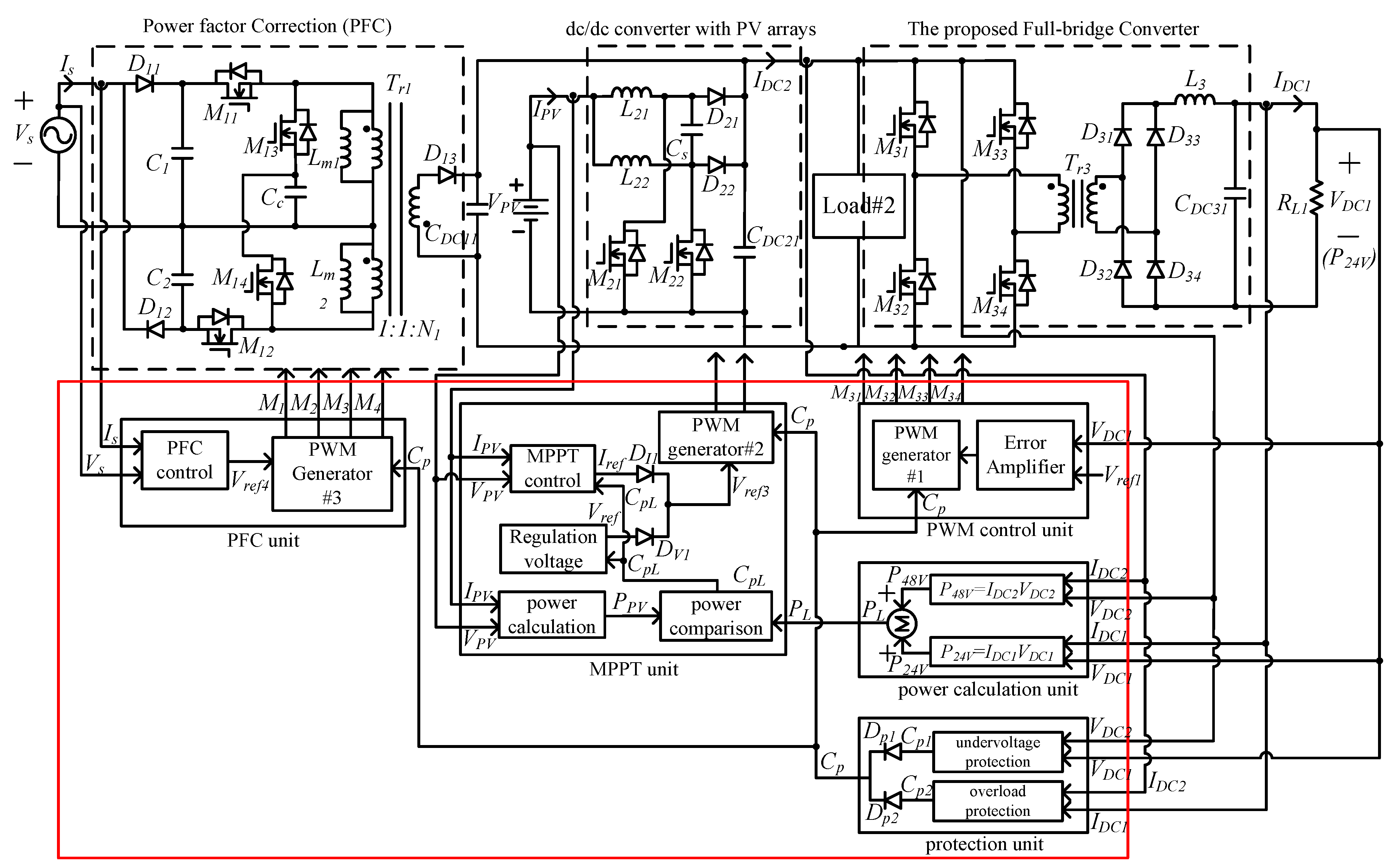
3.1. Topology of the Proposed DC Distribution System
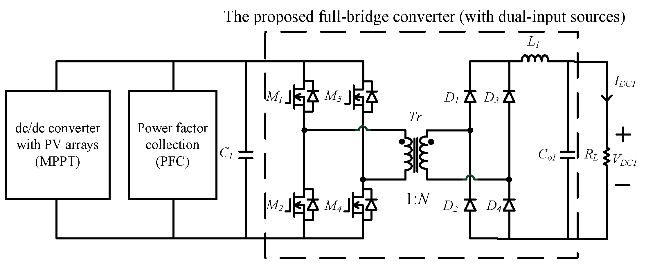
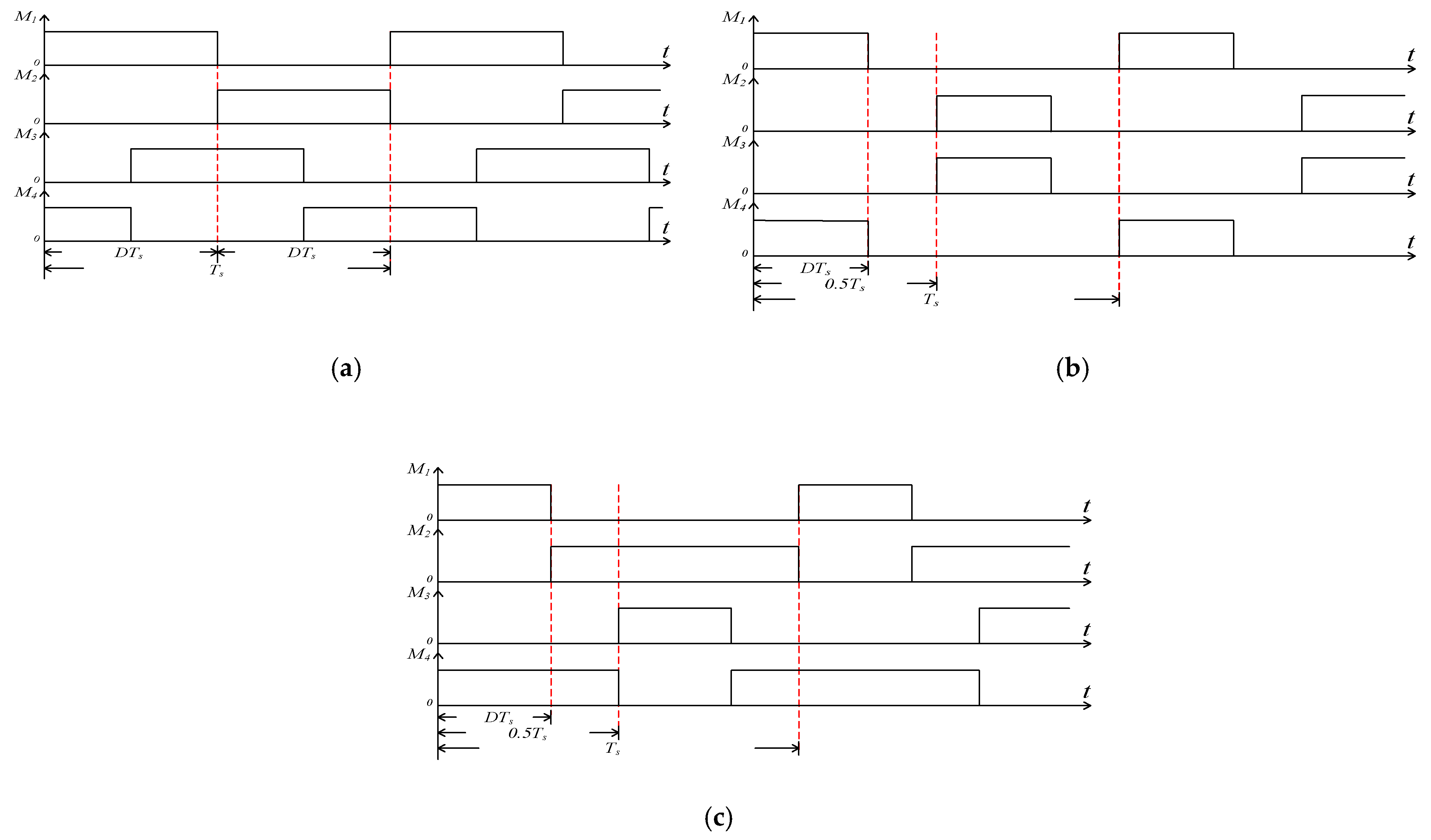
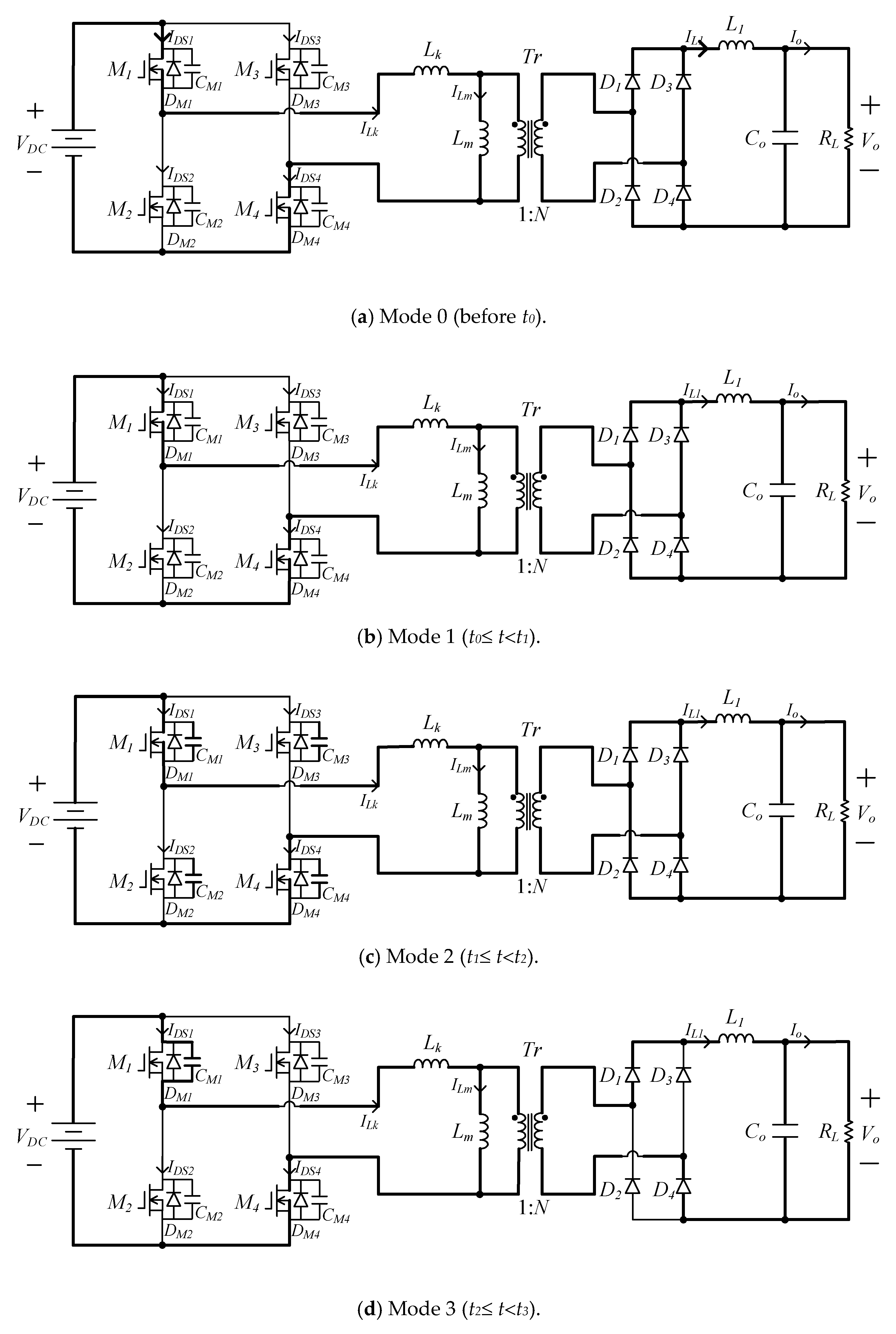
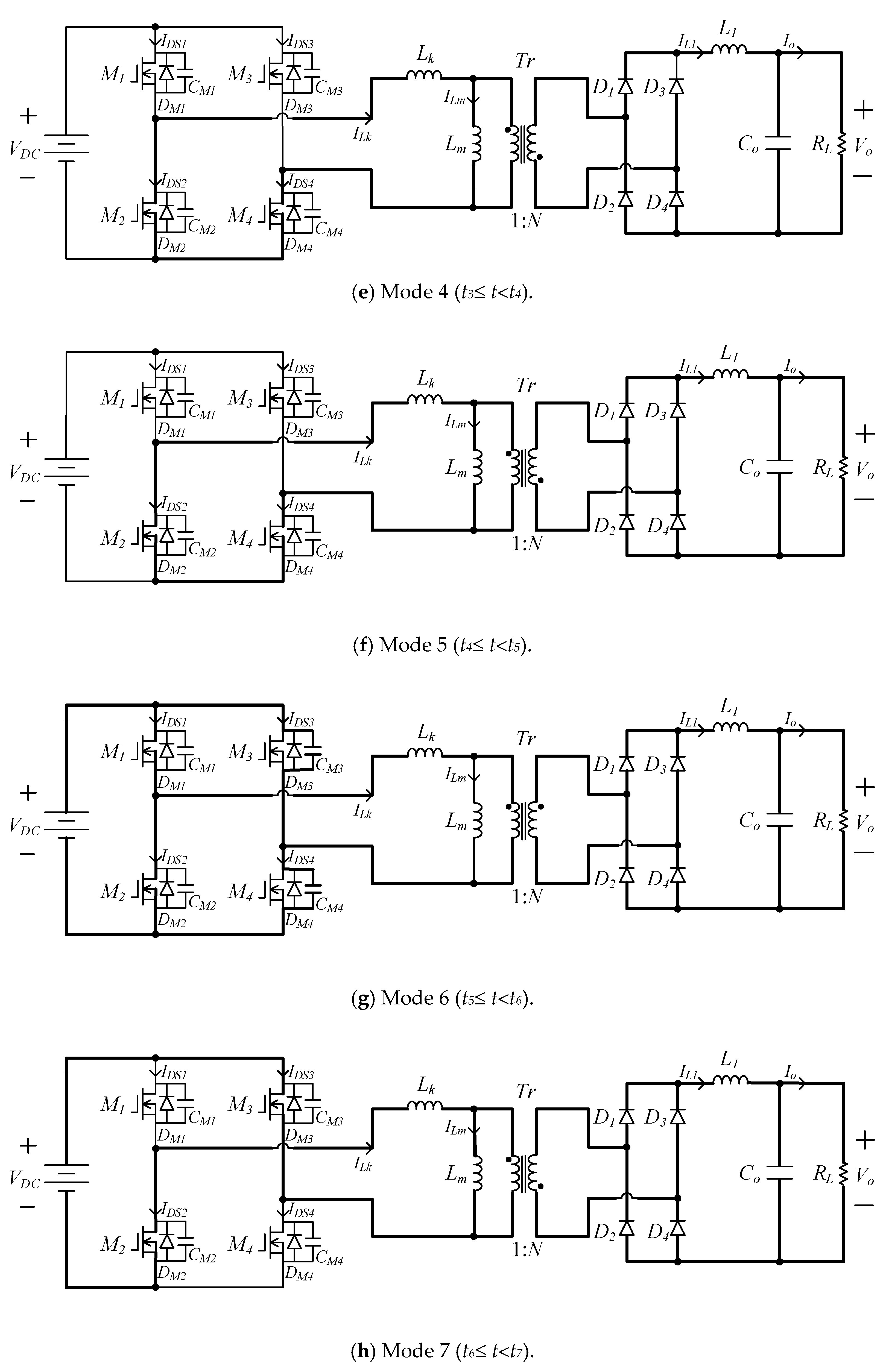
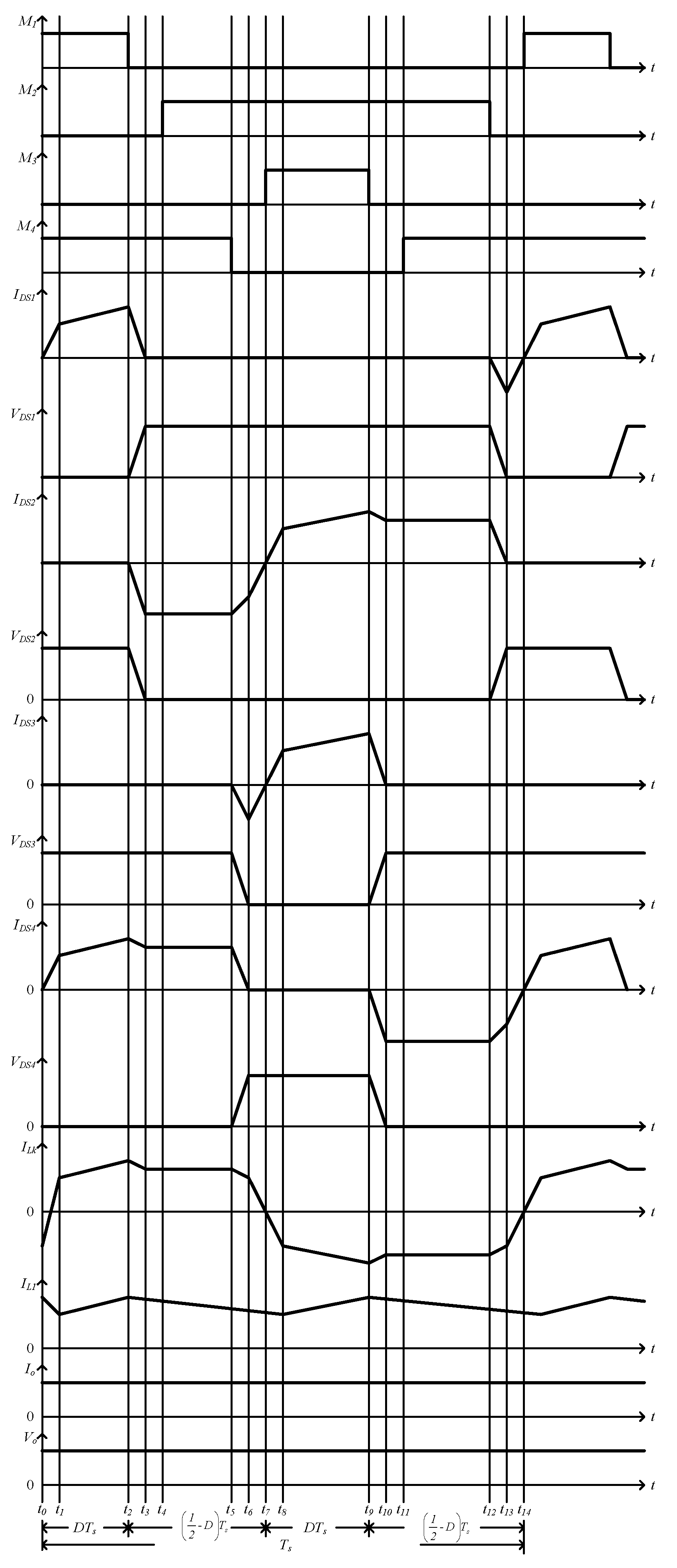
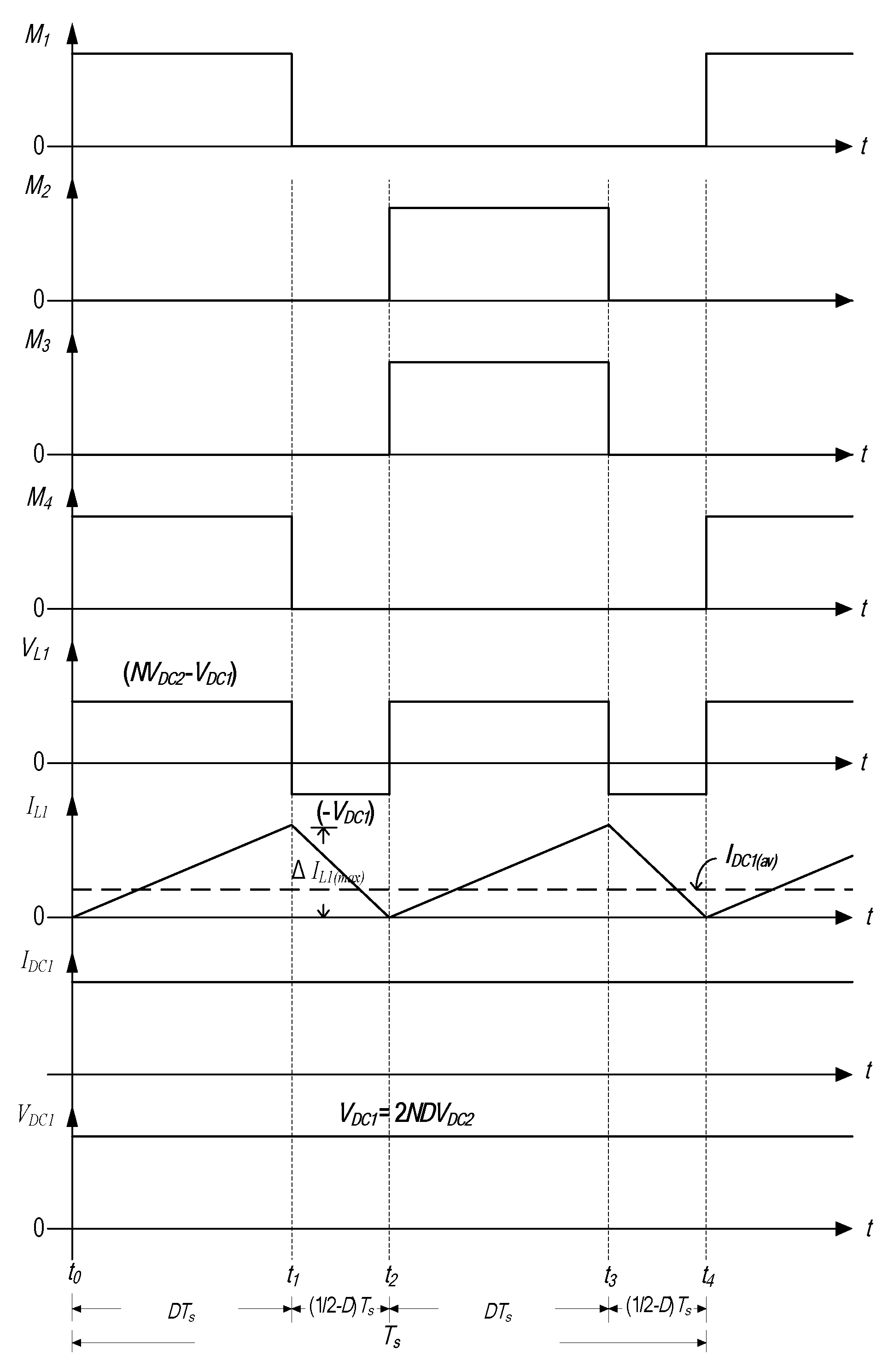
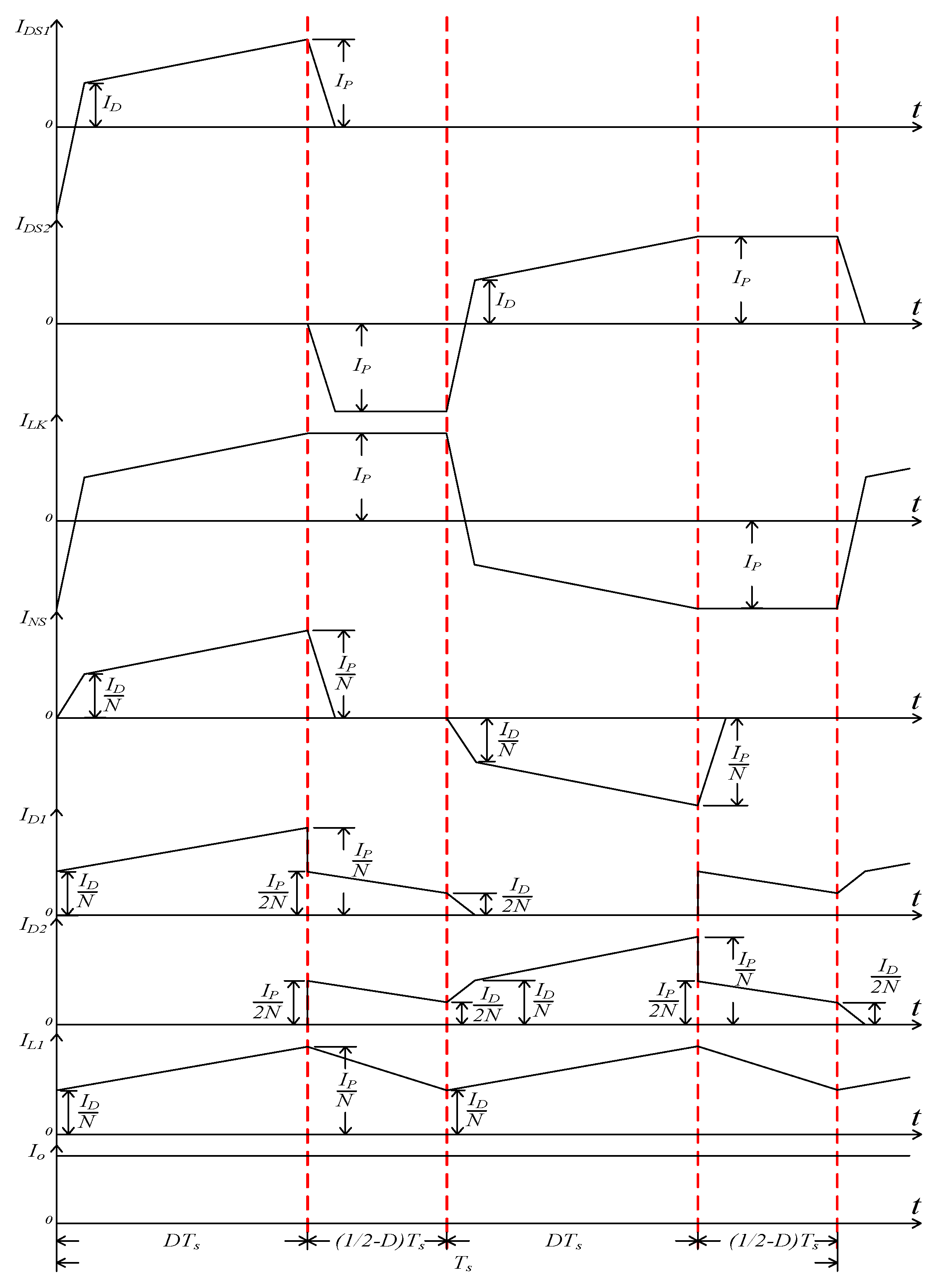
3.2. Operational Method of the Proposed Full-Bridge Converter
4. Design Method of Full-Bridge Converter with Multiple Input Sources
4.1. Component Design of the Proposed Full-Bridge Converter
- (a)
- Duty ratio D
- (b)
- Turns ratio N of Transformer Tr
- (c)
- Inductor L1
- (d)
- Output capacitor CDC1
4.2. Component Selection of the Proposed Full-Bridge Converter
5. Power Loss Analysis of the Proposed Full-Bridge Converter
5.1. Losses of Switches
5.2. Losses of Diodes
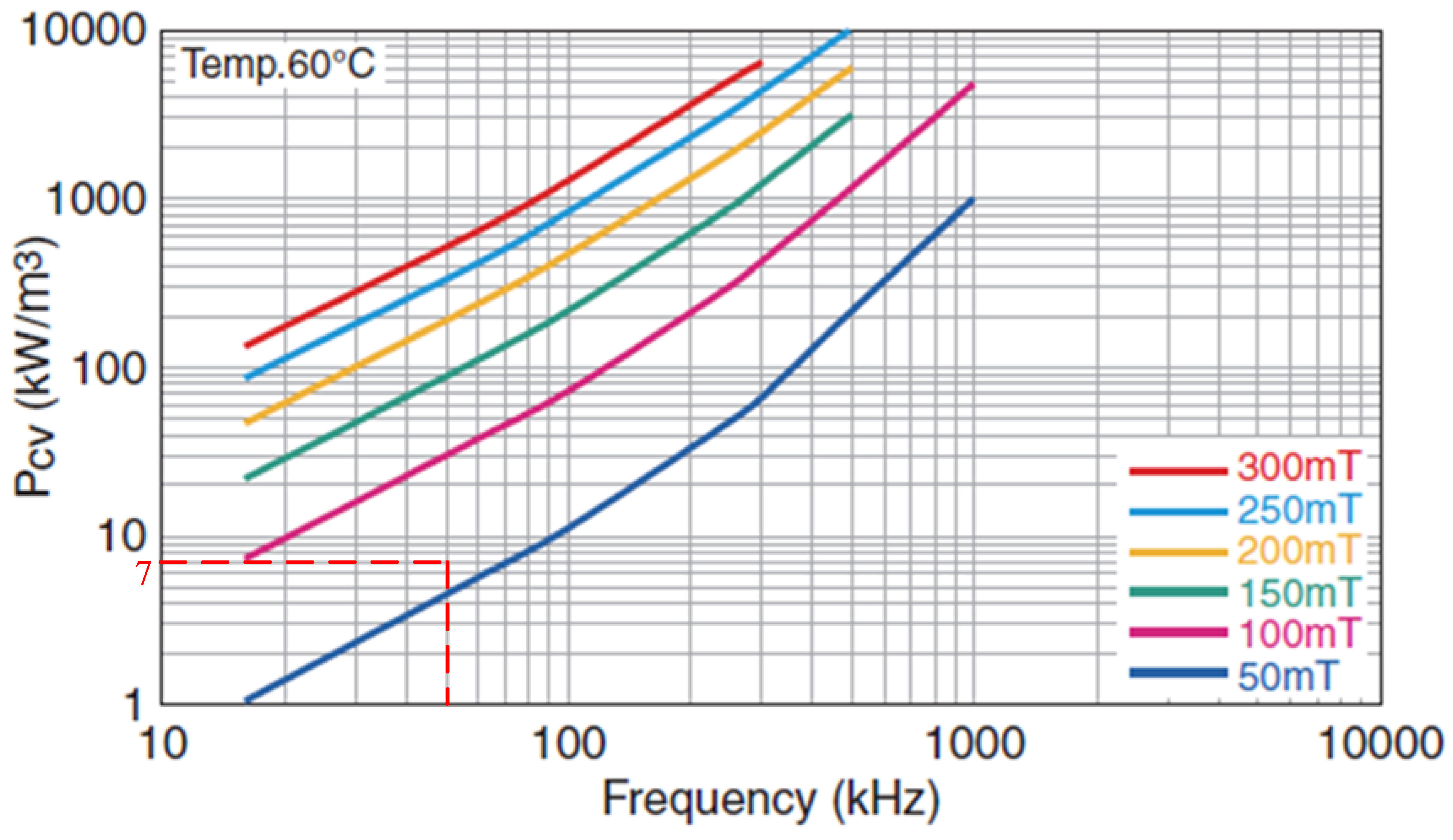
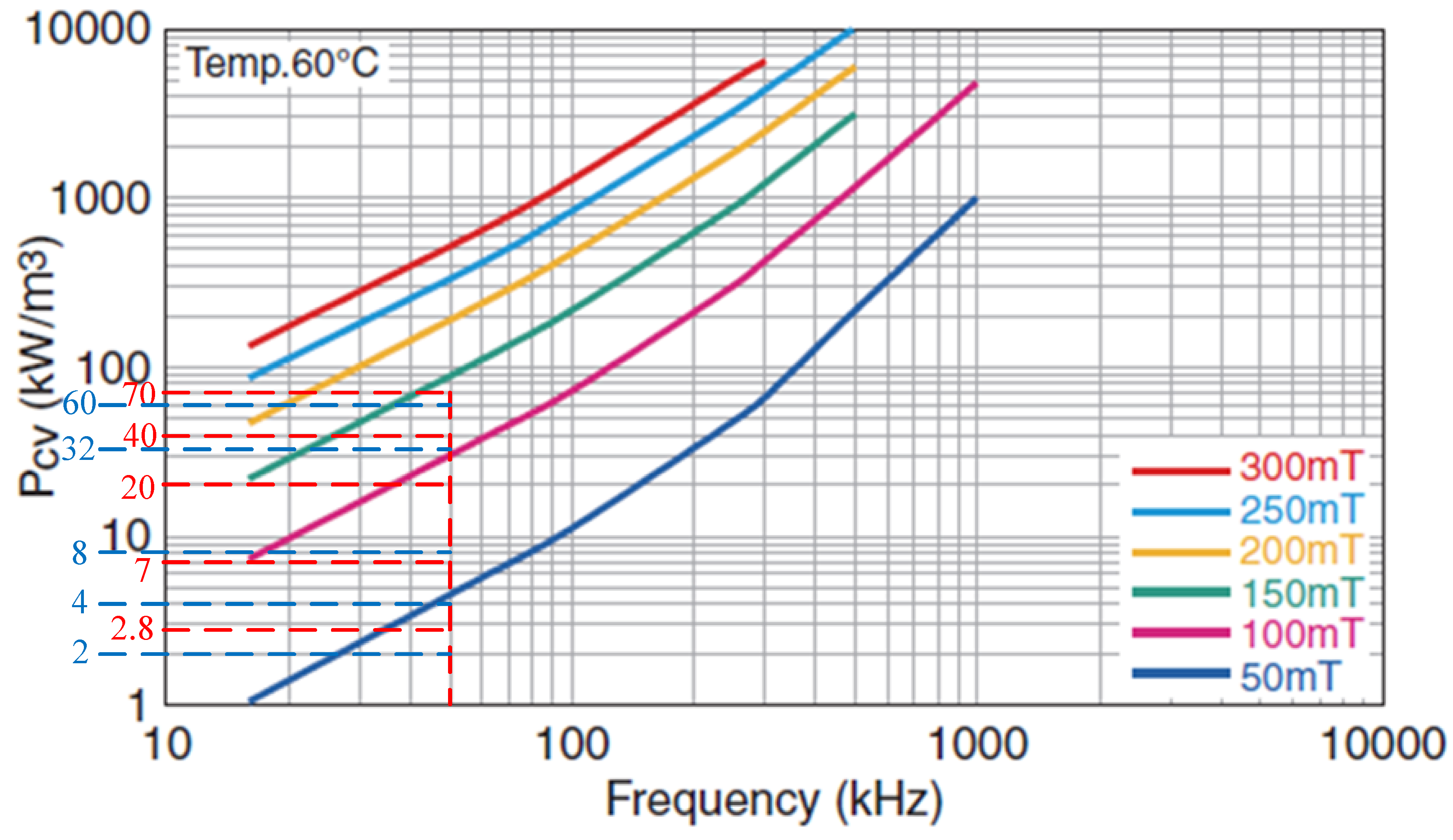
5.3. Losses of Transformer and Inductor
- (a)
- Transformer
- (b)
- Inductor
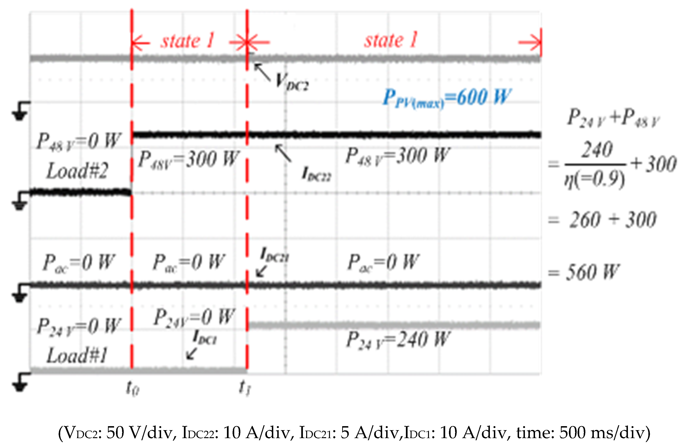
6. Power Management of the Proposed DC Distribution System
6.1. Control Algorithm of the Proposed DC Distribution System
6.2. Power Management of the Proposed DC Distribution System
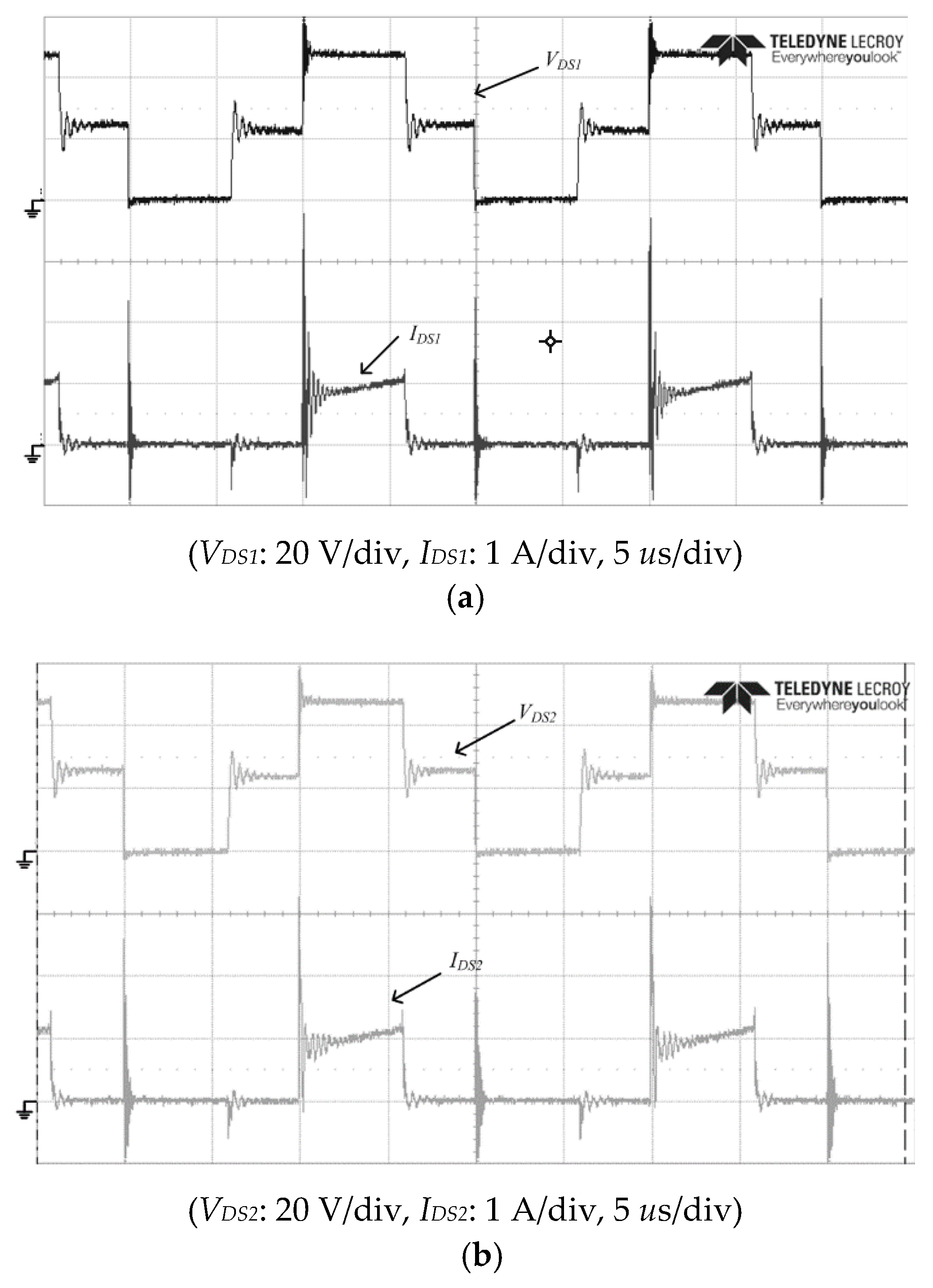
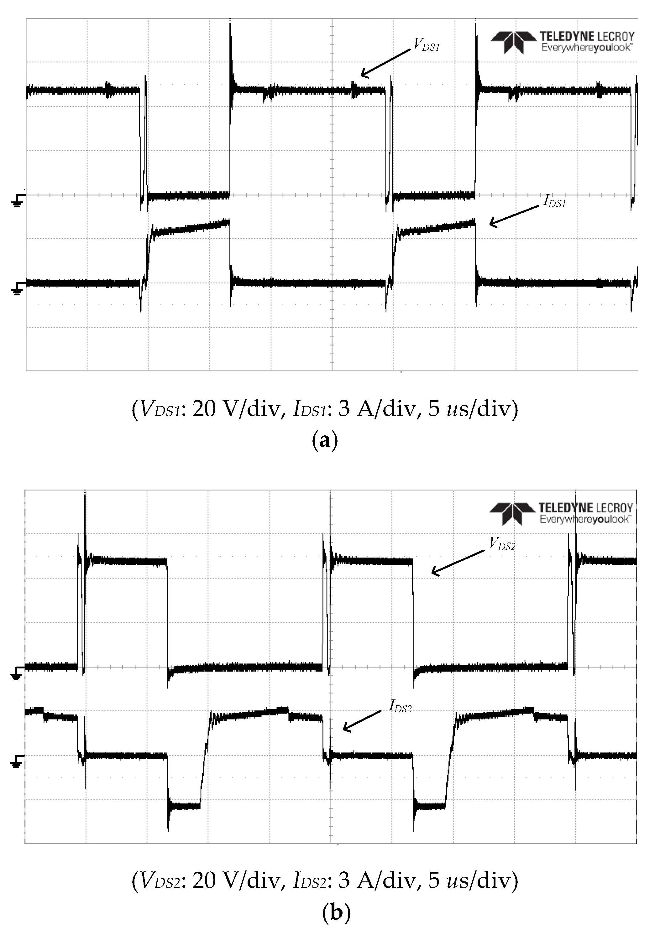
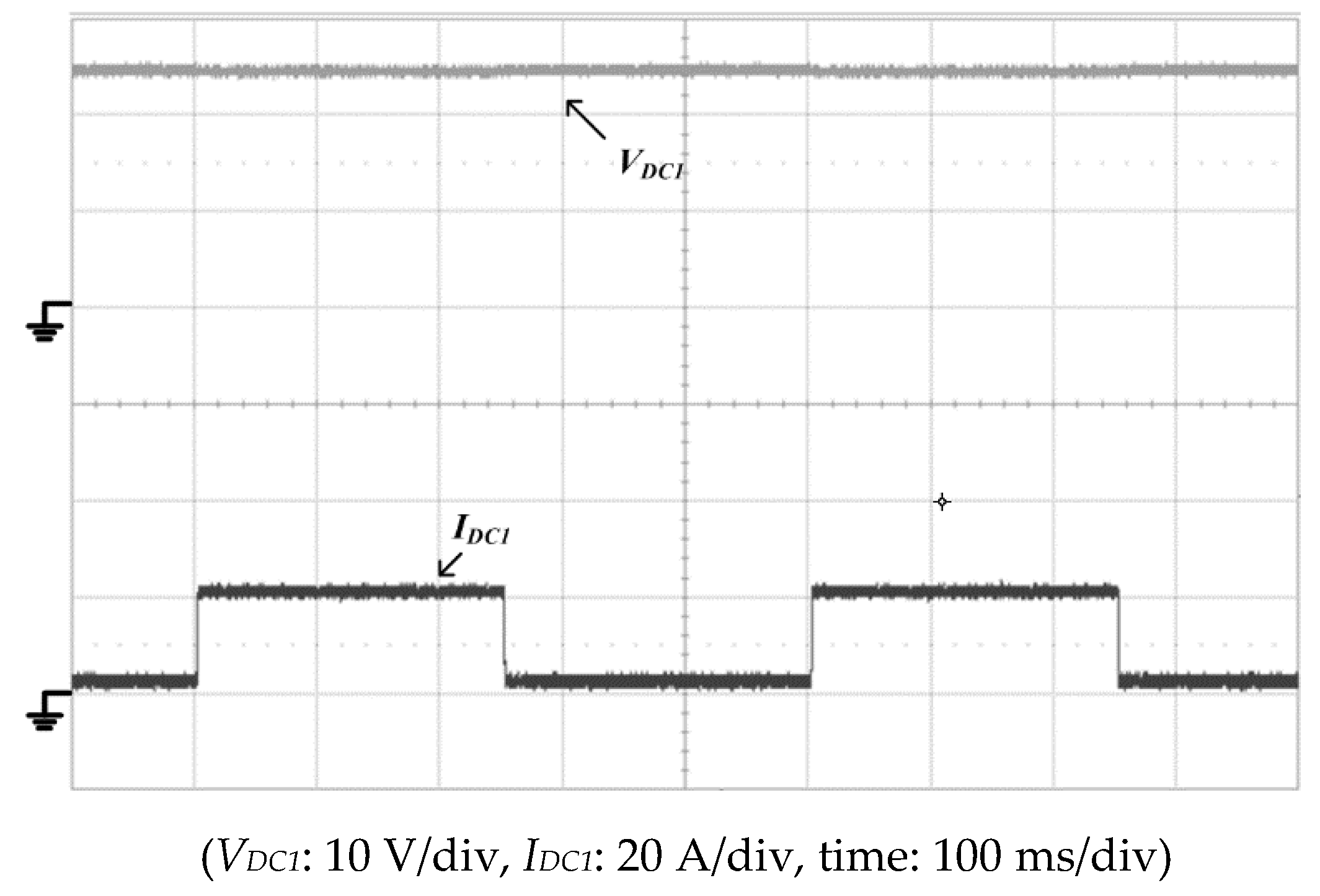
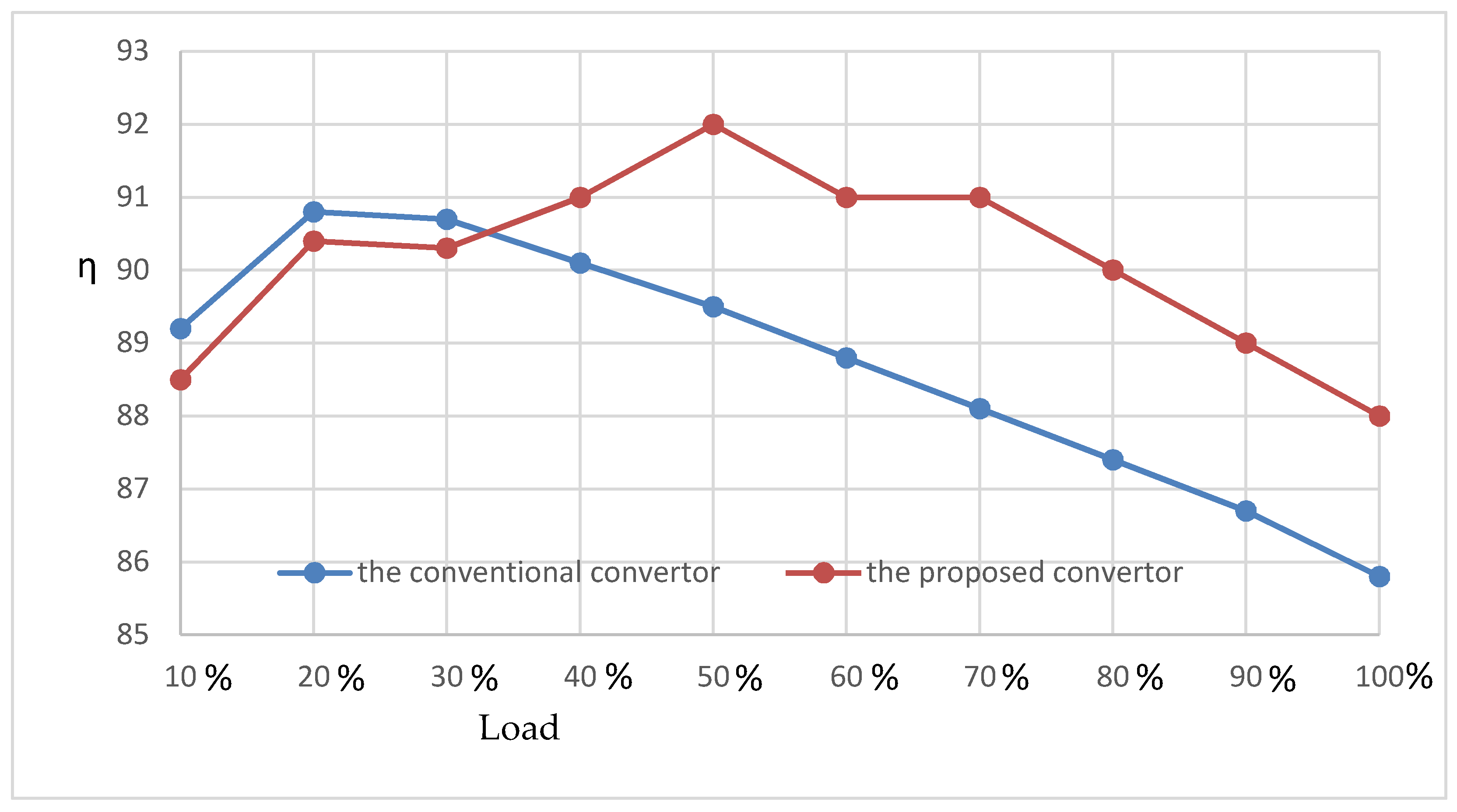
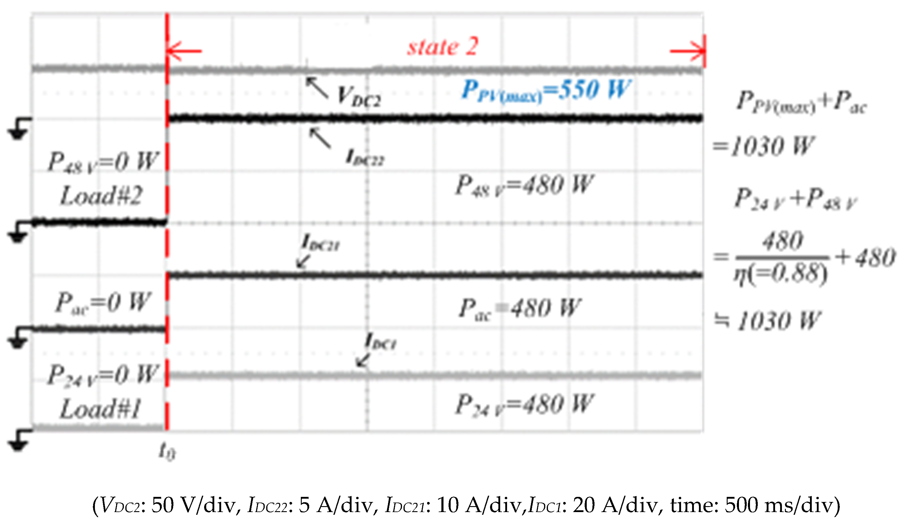
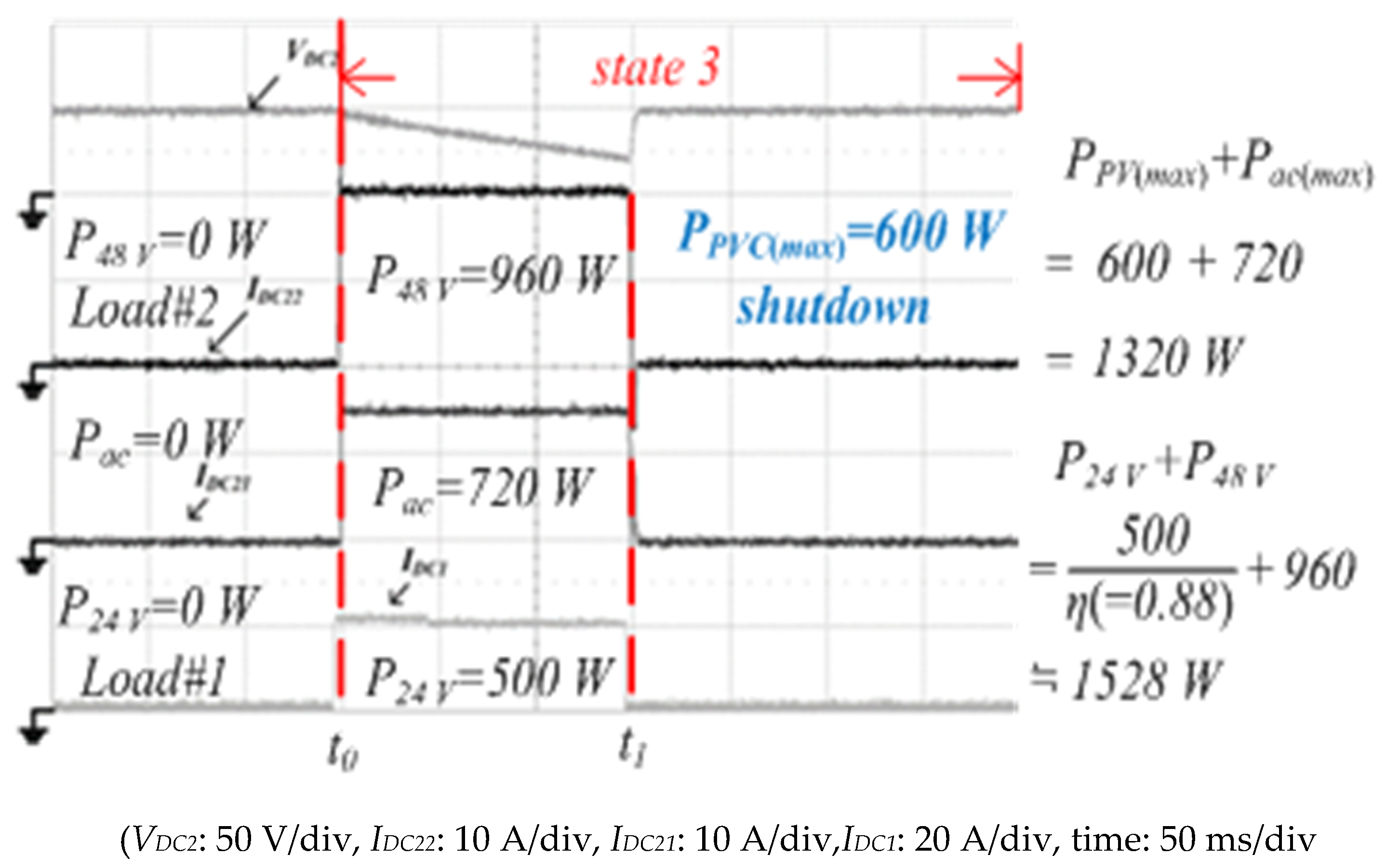
7. Measured Results and Discussion
- Input voltage VDC2: DC 48 V,
- Switching frequency fs: 50 kHz,
- Output voltage VDC1: DC 24 V,
- Maximum output current IDC1(max): 21 A,
- Maximum output power P24SV(max): 500 W.
- Switches M1~M4: AoW2918,
- Transformer core: EE-55,
- Diodes D1~D4: STPS41H100CT,
- Capacitor CDC1: 3300 μF/35 V,
- Leakage inductor LK: 3.8 μH,
- Magnetizing inductor Lm: 1.72 mH.
8. Conclusions
Author Contributions
Funding
Institutional Review Board Statement
Informed Consent Statement
Data Availability Statement
Conflicts of Interest
References
- Singh, S.; Singh, B.; Bhuvaneswari, G.; Bist, V. Power corrected bridgeless converter based switched mode power supply factor. IET Power Electron. 2016, 9, 1684–1693. [Google Scholar] [CrossRef]
- Singh, S.; Bist, V.; Singh, B.; Bhuvaneswari, G. Power factor correction in switched mode power supply for computers using canonical switching cell converter. IET Power Electron. 2015, 8, 234–244. [Google Scholar] [CrossRef]
- Prabhala, V.A.K.; Baddipadiga, B.P.; Ferdowsi, M. DC Distribution Systems—An Overview. In Proceedings of the 2014 International Conference on Renewable Energy Research and Application (ICRERA), Milwaukee, WI, USA, 19–22 October 2014; pp. 307–312. [Google Scholar]
- Zeni, L.; Gevorgian, V.; Wallen, R.; Bech, J.; Sørensen, P.E.; Hesselbæk, B. Utilisation of real-scale renewable energy test facility for validation of generic wind turbine and wind power plant controller models. IET Renew. Power Gener. 2016, 10, 1123–1131. [Google Scholar] [CrossRef]
- Othman, M.M.; Abdelaziz, A.Y.; Hegazi, Y.G.; El-Khattam, W. Approach for modelling stochastically dependent renewable energy-based generators using diagonal band copula. IET Renew. Power Gener. 2015, 9, 809–820. [Google Scholar] [CrossRef]
- Shen, C.L.; Chiu, P.C. Buck-boost-flyback integrated converter with single switch to achieve high voltage gain for PV or fuel-cell applications. IET Power Electron. 2016, 9, 1228–1237. [Google Scholar] [CrossRef]
- Poshtkouhi, S.; Trescases, O. Flyback Mode for Improved Low-Power Efficiency in the Dual-Active-Bridge Converter for Bidirectional PV Microinverters with Integrated Storage. IEEE Trans. Ind. Appl. 2015, 51, 3316–3324. [Google Scholar] [CrossRef]
- Edwin, F.F.; Xiao, W.; Khadkikar, V. Dynamic Modeling and Control of Interleaved Flyback Module-Integrated Converter for PV Power Applications. IEEE Trans. Ind. Electron. 2013, 61, 1377–1388. [Google Scholar] [CrossRef]
- Tamyurek, B.; Kirimer, B. An Interleaved High-Power Flyback Inverter for Photovoltaic Applications. IEEE Trans. Power Electron. 2015, 30, 3228–3241. [Google Scholar] [CrossRef]
- Thangavelu, A.; Senthilkumar, V.; Parvathyshankar, D. Zero voltage switching-pulse width modulation technique-based interleaved flyback converter for remote power solutions. IET Power Electron. 2016, 9, 1381–1390. [Google Scholar] [CrossRef]
- Li, J.; Van Horck, F.B.M.; Daniel, B.J.; Bergveld, H.J. A High-Switching-Frequency Flyback Converter in Resonant Mode. IEEE Trans. Power Electron. 2017, 32, 8582–8592. [Google Scholar] [CrossRef]
- Hwu, K.I.; Tu, W.C.; Wang, C.R. Photovoltaic Energy Conversion System Constructed by High Step-Up Converter with Hybrid Maximum Power Point Tracking. Int. J. Photoenergy 2013, 2013, 1–9. [Google Scholar] [CrossRef]
- Kim, R.-Y.; Lai, J.-S. A Seamless Mode Transfer Maximum Power Point Tracking Controller for Thermoelectric Generator Applications. IEEE Trans. Power Electron. 2008, 23, 2310–2318. [Google Scholar] [CrossRef]
- Weddell, A.S.; Merrett, G.V.; Bashir, M.A.-H. Photovoltaic Sample-and-Hold Circuit Enabling MPPT Indoors for Low-Power Systems. IEEE Trans. Circuits Syst. I Reg. Pap. 2011, 59, 1196–1204. [Google Scholar] [CrossRef] [Green Version]
- Batzelis, E.I.; Kampitsis, G.E.; Papathanassiou, S.A. Power Reserves Control for PV Systems with Real-Time MPP Estimation via Curve Fitting. IEEE Trans. Sustain. Energy 2017, 8, 1269–1280. [Google Scholar] [CrossRef]
- Shen, C.-L.; Yang, S.-H. Multi-Input Converter with MPPT Feature for Wind-PV Power Generation System. Int. J. Photoenergy 2013, 2013, 1–13. [Google Scholar] [CrossRef]
- Leyva, R.; Olalla, C.; Zazo, H.; Cabal, C.; Cid-Pastor, A.; Queinnec, I.; Alonso, C. MPPT Based on Sinusoidal Extremum-Seeking Control in PV Generation. Int. J. Photoenergy 2012, 2012, 1–7. [Google Scholar] [CrossRef]
- Thangavelu, A.; Vairakannu, S.; Parvathyshankar, D. Linear open circuit voltage-variable step-size-incremental conductance strategy-based hybrid MPPT controller for remote power applications. IET Power Electron. 2017, 10, 1363–1376. [Google Scholar] [CrossRef]
- Huynh, D.C.; Dunnigan, M.W. Development and Comparison of an Improved Incremental Conductance Algorithm for Tracking the MPP of a Solar PV Panel. IEEE Trans. Sustain. Energy 2016, 7, 1421–1429. [Google Scholar] [CrossRef]
- Lark, H. Asymmetrical Full-bridge Converter with High-Voltage Gain. IEEE Power Electron. 2012, 27, 860–868. [Google Scholar]
- Haijun, T.; Yiming, Z.; Xiguo, R. Full-Bridge DC-DC Converter Using Asymmetric Phase-Shifted PWM Control. Open Autom. Control. Syst. J. 2015, 7, 1909–1915. [Google Scholar] [CrossRef] [Green Version]
- Chen, Z.; Liu, S.; Shi, L. A Soft Switching Full Bridge Converter with Reduced Parasitic Oscillation in a Wide Load Range. IEEE Power Electron. 2014, 29, 801–811. [Google Scholar] [CrossRef]
- Pahlevaninezhad, M.; Das, P.; Drobnik, J.; Jain, P.K.; Bakhshai, A. A Novel ZVZCS Full-Bridge DC/DC Converter Used for Electric Vehicles. IEEE Trans. Power Electron. 2012, 27, 2752–2769. [Google Scholar] [CrossRef]
- Moschopoulos, G.; Jain, P. Single-stage ZVS PWM full-bridge converter. IEEE Trans. Aerosp. Electron. Syst. 2003, 39, 1122–1133. [Google Scholar] [CrossRef]
- Choi, W.-Y.; Yang, M.-K.; Cho, H.-S. High-Frequency-Link Soft-Switching PWM DC–DC Converter for EV On-Board Battery Chargers. IEEE Trans. Power Electron. 2014, 29, 4136–4145. [Google Scholar] [CrossRef]
- Dudrik, J.; Bodor, M.; Pastor, M. Soft-Switching Full-Bridge PWM DC–DC Converter with Controlled Output Rectifier and Secondary Energy Recovery Turn-Off Snubber. IEEE Trans. Power Electron. 2013, 29, 4116–4125. [Google Scholar] [CrossRef]
- Wijeratne, D.; Moschopoulos, G. A ZVS-PWM full-bridge converter with reduced conduction losses. In Proceedings of the 2011 Twenty-Sixth Annual IEEE Applied Power Electronics Conference and Exposition (APEC), Fort Worth, TX, USA, 6–11 March 2011; Volume 29, pp. 864–870. [Google Scholar]
- Wang, H.; Sun, Q.; Chung, H.S.H.; Tapuchi, S.; Ioinovici, A. A ZCS current-fed full-bridge PWM converter with self-adaptable SoftSwitching snubber energy. IEEE Power Electron. 2009, 24, 1977–1991. [Google Scholar] [CrossRef]


| Acronyms/ Abbreviations | Parameter/Definition |
|---|---|
| ZVS | Zero-voltage switching |
| PFC | Power factor correction |
| ZCS | Zero-current switching |
| ZCT | Zero-current transition |
| ZVT | Zero-voltage transition |
| IC | Integrated circuit |
| PWM | Pulse-width modulation |
| PV | Photovoltaic |
| MPPT | Maximum power point tracking |
| CCM | Continuous conduction mode |
| DCM | Discontinuous conduction mode |
| Component | Part Number | Voltage/Current Ratings or Formula | Features | ||
|---|---|---|---|---|---|
| Symbol | Parameter | Values | |||
| Switches , , , | AOW2918 | 100 V/90 A | Drain-source on resistance | <7 mΩ | |
| Turn-on transition time | 41 ns | ||||
| Turn-off transition time | 51 ns | ||||
| Diodes ~ | STPS41H100CT | 100 V/40 A | Maximum forward voltage | 0.67 V | |
| Transformer | EE-55Core (PC 40, manufactured by TDK) | (T) : 4π× : Peak Current of magnetizing inductor for primary winding (Ω) (Ω) | Permeability | 2300 | |
| Effective Magnetic Path length | 123 mm | ||||
| Effective core volume | 43.7 | ||||
| Approximate mean length of turn for primary winding | 92.2 mm | ||||
| Approximate mean length of turn for secondary winding | 100.6 mm | ||||
| Resistance using 40 strands of AWG#28 for primary winding | 8.37 mΩ | ||||
| Resistance using 80 strands of AWG#28 for secondary winding | 3.71 mΩ | ||||
| Turn of primary winding | 16 T | ||||
| Turn of secondary winding | 13 T | ||||
| Resistance of AWG#28 | 227 | ||||
| Inductor | EE-55Core (PC 40 manufactured by TDK) | (T) : Peak Current of inductor (Ω) | permeability | 2300 | |
| Effective Magnetic Path length | 123 mm | ||||
| Effective core volume | 43.7 | ||||
| Approximate mean length of turn | 96.4 mm | ||||
| Resistance using 80 strands of AWG#28 | 4.38 mΩ | ||||
| Air gap | 3.08 mm | ||||
| Turn of inductor | 16 T | ||||
| Operating States | State 1 | State 2 | State 3 | |
|---|---|---|---|---|
| Power System | ||||
| Power factor correction (utility line) Pac(max) | shutdown | working | shutdown | |
| DC/DC converter with PV arrays (MPPT) PPV(max) | working | working | shutdown | |
| The proposed full-bridge converter (with multiple input sources) | working | working | shutdown | |
| Load#1 | ON | ON | OFF | |
| Load#2 | ON | ON | OFF | |
| Load (%) | |||||
|---|---|---|---|---|---|
| Switch Loss | Conduction Loss | Switching Loss | Conduction Loss | Forward Drop | |
| 10 | 160 m | 7 m | 160 m | 25 m | 0.76 |
| 20 | 263 m | 25 m | 263 m | 36 m | 1.47 |
| 30 | 365 m | 56 m | 365 m | 150 m | 2.19 |
| 40 | 468 m | 99 m | 468 m | 253 m | 2.91 |
| 50 | 571 m | 155 m | 571 m | 384 m | 3.63 |
| 60 | 674 m | 223 m | 674 m | 541 m | 4.36 |
| 70 | 777 m | 303 m | 777 m | 726 m | 5.08 |
| 80 | 880 m | 396 m | 880 m | 938 m | 5.81 |
| 90 | 982 m | 501 m | 982 m | 1.18 | 6.53 |
| 100 | 1.085 | 618 m | 1.085 | 1.44 | 7.26 |
| Load (%) | (A) | (A) | (A) | Operational Condition | ||||||
|---|---|---|---|---|---|---|---|---|---|---|
| 10 | 2.1 | 0.75 | 2.611 | 0.986 | 1.879 | 2.122 | 1.743 | 1.136 | 2.205 | , , , , , , , , , and = 0.174 A |
| 20 | 4.2 | 2.43 | 4.291 | 1.902 | 2.269 | 3.76 | 3.362 | 2.192 | 4.253 | |
| 30 | 6.3 | 4.11 | 5.971 | 2.834 | 4.626 | 5.425 | 5.01 | 3.266 | 6.337 | |
| 40 | 8.4 | 5.79 | 7.651 | 3.769 | 6.013 | 7.097 | 6.663 | 4.344 | 8.428 | |
| 50 | 10.5 | 7.47 | 9.331 | 4.706 | 7.402 | 8.772 | 8.319 | 5.423 | 10.523 | |
| 60 | 12.6 | 9.15 | 11.011 | 5.643 | 8.793 | 11.448 | 9.976 | 6.563 | 12.618 | |
| 70 | 14.7 | 10.83 | 12.691 | 6.581 | 10.184 | 12.125 | 11.634 | 7.584 | 14.716 | |
| 80 | 16.8 | 12.51 | 14.371 | 7.519 | 11.575 | 13.803 | 13.292 | 8.665 | 16.813 | |
| 90 | 18.9 | 14.19 | 16.051 | 8.458 | 12.967 | 15.482 | 14.952 | 9.747 | 18.913 | |
| 100 | 21 | 15.87 | 17.731 | 9.397 | 14.36 | 17.161 | 16.612 | 10.829 | 21.012 |
| Load (%) | Core Loss and Core Parameters | |||||||
|---|---|---|---|---|---|---|---|---|
| Maximum Flux Density | Core Loss Efficiency | Core Loss (W) | Copper Loss | Maximum Flux Density | Core Loss Efficiency | Core Loss (W) | Copper Loss | |
| 10 | 65.3 | 7 | 306 m | 49 m | 20.9 | 2 | 87 m | 21 m |
| 20 | 65.3 | 7 | 306 m | 160 m | 34.4 | 2.8 | 122 m | 79 m |
| 30 | 65.3 | 7 | 306 m | 339 m | 47.9 | 4 | 175 m | 176 m |
| 40 | 65.3 | 7 | 306 m | 586 m | 61.3 | 7 | 360 m | 311 m |
| 50 | 65.3 | 7 | 306 m | 900 m | 74.8 | 8 | 350 m | 485 m |
| 60 | 65.3 | 7 | 306 m | 1.47 | 88.2 | 20 | 874 m | 697 m |
| 70 | 65.3 | 7 | 306 m | 1.73 | 101.7 | 32 | 1.40 | 949 m |
| 80 | 65.3 | 7 | 306 m | 2.25 | 115.2 | 40 | 1.75 | 1.24 |
| 90 | 65.3 | 7 | 306 m | 2.84 | 128.6 | 60 | 2.62 | 1.57 |
| 100 | 65.3 | 7 | 306 m | 3.49 | 142.1 | 70 | 3.06 | 1.93 |
| Load (%) | Practical Efficiency (%) | Switch Losses | Diode Losses | Total Core Losses | Total Power Losses | Calculation Efficiency | |
|---|---|---|---|---|---|---|---|
| Switching Losses | Conduction Loss | ||||||
| 10 | 88.5 | 640 m | 64 m | 3.04 | 463 m | 4.21 | 92.2 |
| 20 | 90.5 | 1.05 | 122 m | 5.88 | 667 m | 7.72 | 92.8 |
| 30 | 90.4 | 1.46 | 412 m | 8.76 | 996 m | 11.63 | 92.8 |
| 40 | 91 | 1.87 | 704 m | 11.64 | 1.56 | 15.77 | 92.7 |
| 50 | 92 | 2.28 | 1.08 | 14.52 | 2.04 | 19.92 | 92.6 |
| 60 | 91 | 2.70 | 1.53 | 17.44 | 3.35 | 25.02 | 92.3 |
| 70 | 91 | 3.11 | 2.06 | 20.32 | 4.39 | 29.88 | 92.1 |
| 80 | 90 | 3.52 | 2.67 | 23.24 | 5.55 | 34.98 | 91.9 |
| 90 | 89 | 3.93 | 3.36 | 26.12 | 7.34 | 40.75 | 91.7 |
| 100 | 88 | 4.34 | 4.11 | 29.04 | 8.79 | 46.28 | 91.5 |
| Power Sources | Symbol | Definition | Value |
|---|---|---|---|
| Utility line (using power factor correction(PFC)) | Pac | output power of utility line at present | |
| Pac(max) | maximum output power of utility line | 720 W | |
| PV arrays (using DC/DC converter with PV arrays) | PPV | output power of PV arrays | |
| PPV(max) | maximum output power of PV arrays | 1200 W | |
| Load | P24 V | consumption power at present (Load#1) | P24 V(max) = 500 W |
| P48 V | consumption power at present (Load#2) | P48 V(max) = 1360 W | |
| P24SV | output power of the proposed full-bridge converter | ||
| P24SV(max) | maximum output power of the proposed full-bridge converter | 500 W |
Publisher’s Note: MDPI stays neutral with regard to jurisdictional claims in published maps and institutional affiliations. |
© 2021 by the authors. Licensee MDPI, Basel, Switzerland. This article is an open access article distributed under the terms and conditions of the Creative Commons Attribution (CC BY) license (https://creativecommons.org/licenses/by/4.0/).
Share and Cite
Tseng, S.-Y.; Fan, J.-H. Soft-Switching Full-Bridge Converter with Multiple-Input Sources for DC Distribution Applications. Symmetry 2021, 13, 775. https://doi.org/10.3390/sym13050775
Tseng S-Y, Fan J-H. Soft-Switching Full-Bridge Converter with Multiple-Input Sources for DC Distribution Applications. Symmetry. 2021; 13(5):775. https://doi.org/10.3390/sym13050775
Chicago/Turabian StyleTseng, Sheng-Yu, and Jun-Hao Fan. 2021. "Soft-Switching Full-Bridge Converter with Multiple-Input Sources for DC Distribution Applications" Symmetry 13, no. 5: 775. https://doi.org/10.3390/sym13050775