Article

Polymer-Doped SnO2 as an Electron Transport Layer for Highly Efficient and Stable Perovskite Solar Cells

Department of Electrical Engineering, Gachon University, Seongnam 13120, Gyeonggi, Republic of Korea
*
Author to whom correspondence should be addressed.
Polymers 2024, 16(2), 199; https://doi.org/10.3390/polym16020199
Submission received: 17 December 2023 / Revised: 5 January 2024 / Accepted: 8 January 2024 / Published: 9 January 2024

Abstract

:
To produce highly efficient and repeatable perovskite solar cells (PSCs), comprehending interfacial loss and developing approaches to ameliorate interfacial features is essential. Nonradiative recombination at the SnO2–perovskite interface in SnO2-based perovskite solar cells (PSCs) leads to significant potential loss and variability in device performance. To improve the quality of the SnO2 electron transport layer, a novel polymer-doped SnO2 matrix, specifically using polyacrylic acid, was developed. This matrix is formed by spin-coating a SnO2 colloidal solution that includes polymers. The polymer aids in dispersing nanoparticles within the substrate and is evenly distributed in the SnO2 solution. As a result of the polymer addition, the density and wetting properties of the SnO2 layer substantially improved. Subsequently, perovskite-based photovoltaic devices comprising SnO2 and Spiro-OMeTAD layers and using (FAPbI3)0.97(MAPbBr3)0.03 perovskite are constructed. These optimized devices exhibited an increased efficiency of 17.2% when compared to the 15.7% power conversion efficiency of the control device. The incorporation of polymers in the electron transport layer potentially enables even better performance in planar perovskite solar cells.

1. Introduction

Metal halide perovskite has emerged as a key technology for high-performance optoelectronic devices, owing to its long diffusion length and high defect tolerance [1,2,3,4]. Recent advancements have seen perovskite solar cells (PSCs) achieve a rapid increase in power conversion efficiency (PCE), reaching up to 26% [5,6,7]. This progress parallels the optimal standard of commercial silicon cells [8]. Planar PSCs are becoming increasingly prominent and competitive in the photovoltaic field due to their simple synthesis process, low cost, and high efficiency [9,10,11,12]. However, challenges such as significant photocurrent hysteresis and unstable output under operational conditions remain major concerns for many planar PSCs [13,14,15]. These issues are largely attributed to ion migration and suboptimal interfacial properties in the devices [16,17]. Many studies have underscored the importance of smooth and dense surfaces for efficient electron transport and effective hole blocking, which prevents holes from moving from the absorber layers to the transparent electrode [18,19]. Consequently, there is a strong consensus on the necessity of designing optimal electron transport.
The ETL plays a vital role in PSC performance. To inhibit carrier recombination, the ETL must simultaneously prevent the migration of carriers to the counter electrode and facilitate the charge transport process from the photoactive layer to the electrode. Specifically, TiO2, ZnO, Nb2O5, Zn2SO4, Fe2O3, In2O3, and SnO2 are widely used ETLs in PSCs. The specific performance of varied types of ETL is presented in detail in Table 1.
Despite an increase in the number of semiconductor materials that are being discovered and applied for ETL in PSC, TiO2 and SnO2 have been extensively used as ETLs due to their superior properties. Mesoporous TiO2 coated over compact TiO2 was initially used as the electron transport material for PSCs, originating from solid-state dye-sensitized solar cells [27]. Nevertheless, the low electron mobility of TiO2 as well as high-temperature annealing have both negative and detrimental effects on the future application of PSCs [28,29,30,31]. Additionally, the strong effects of photocatalytic TiO2 require special attention because they reduce the stability of PSC under illumination [32,33]. Recently, SnO2 has been widely used as the most promising ETL, with a proven efficiency of over 21% and a substantial reduction in photocatalytic and hysteresis issues under illumination [34,35]. SnO2 exhibits the typical properties of an ideal ETL with high mobility [up to 240 cm2/(V·s)], large bandgap (exceeding 3.6 eV), and excellent chemical stability, making it a strong candidate for highly efficient PSCs [36,37]. However, SnO2 is inherently an insulating material when processed at low temperatures, and the efficiency of the device is heavily dependent on the thickness of the SnO2 layer [38,39,40,41]. To achieve fast charge transfer, high-performance SnO2-based PSCs require a thin SnO2 layer that is less than 30 nm in thickness. The aggregation issue of the nanoparticles in the film makes it difficult to fabricate such a thin and compact layer using the spin-coating technique [42,43,44]. Typically, the resulting SnO2 thin film has extensive areas of nonuniformity and pinholes. Additionally, pretreatment (such as UV treatment) is necessary to change the poor wetting performance of SnO2 with the perovskite precursor solution.
Doping organic compounds into electron transport layers (ETLs) can either align the Fermi level of the ETL with the conduction band of perovskite or influence the perovskite/hole transport layers, improving the crystallization and grain size of the perovskite layer [45,46,47]. Thus, doping effectively lowers trap defects in the photo absorber and ETL, enhancing charge separation and transfer for efficient perovskite solar cell performance. Based on this approach, polyethylenimine ethoxylate (PEIE) was utilized to enhance the electron transport capacity of SnO2 by suppressing trap-assisted recombination and lowering the energy barrier between the active layer, as well as improving the wetting ability of these layers, resulting in high PSC performance [48]. Additionally, incorporating polyethylene glycol (PEG) promoted the separation of nanoparticles in the film and significantly improved the density and wetting properties of the SnO2 layer, leading to an improvement in device performance [49]. Furthermore, polyvinyl pyrrolidone (PVP), another water-soluble polymer, was also used for this purpose [50]. The formation of bonds between the electron pairs of nitrogen (or oxygen) in PVP and metal ions enables PVP to adhere to metal surfaces, while the long vinyl polymer chain of the PVP backbone prevents nanoparticle agglomeration through steric hindrance [50].
Given these challenges, doping the ETL with polymers to create a uniform and compact SnO2 ETL and enhance the PCE of devices is valuable. PAA polymer has been extensively used in various energy storage technologies, such as electrolytes in flexible symmetrical supercapacitors, novel separators in silver oxide batteries, or as binders for GaP anodes in lithium-ion batteries [51,52,53]. However, the use of PAA as a doping material in SnO2 colloidal precursors for PSCs has not been explored. We propose that integrating PAA with the SnO2 colloidal solution could help in forming an effective ETL. Additionally, we present the development of an ideal PAA@SnO2 ETL, combining SnO2 with Li-ion. By selecting water-soluble polymers such as PAA, which dissolve in the SnO2 colloidal aqueous solution, we discovered that the PAA chain effectively limits the aggregation of SnO2 nanoparticles in the precursor solution. This combination with polymers substantially improves the quality of the film, enhancing its compaction and wetting properties.

2. Experiment Section

2.1. Materials

Lead Iodide (PbI2), Lithium chloride (LiCl), spiro-oMeTAD (99.8%), methylammonium bromide (MABr), methylammonium chloride (MACl), chlorobenzene (CB), isopropanol (IPA), DMSO, DMF, acetonitrile (ACN), lithium bis(trifluoromethanesulfonyl) imide (Li-TFSI), and 4-tert-butyl were purchased from Sigma-Aldrich (Seoul, Republic of Korea). A SnO2 colloidal solution (15 wt% in water) was purchased from Alfa Aesar (Seoul, Republic of Korea). Formamidinium iodide (FAI) was purchased from GreatCell Solar (Queanbeyan, Australia).

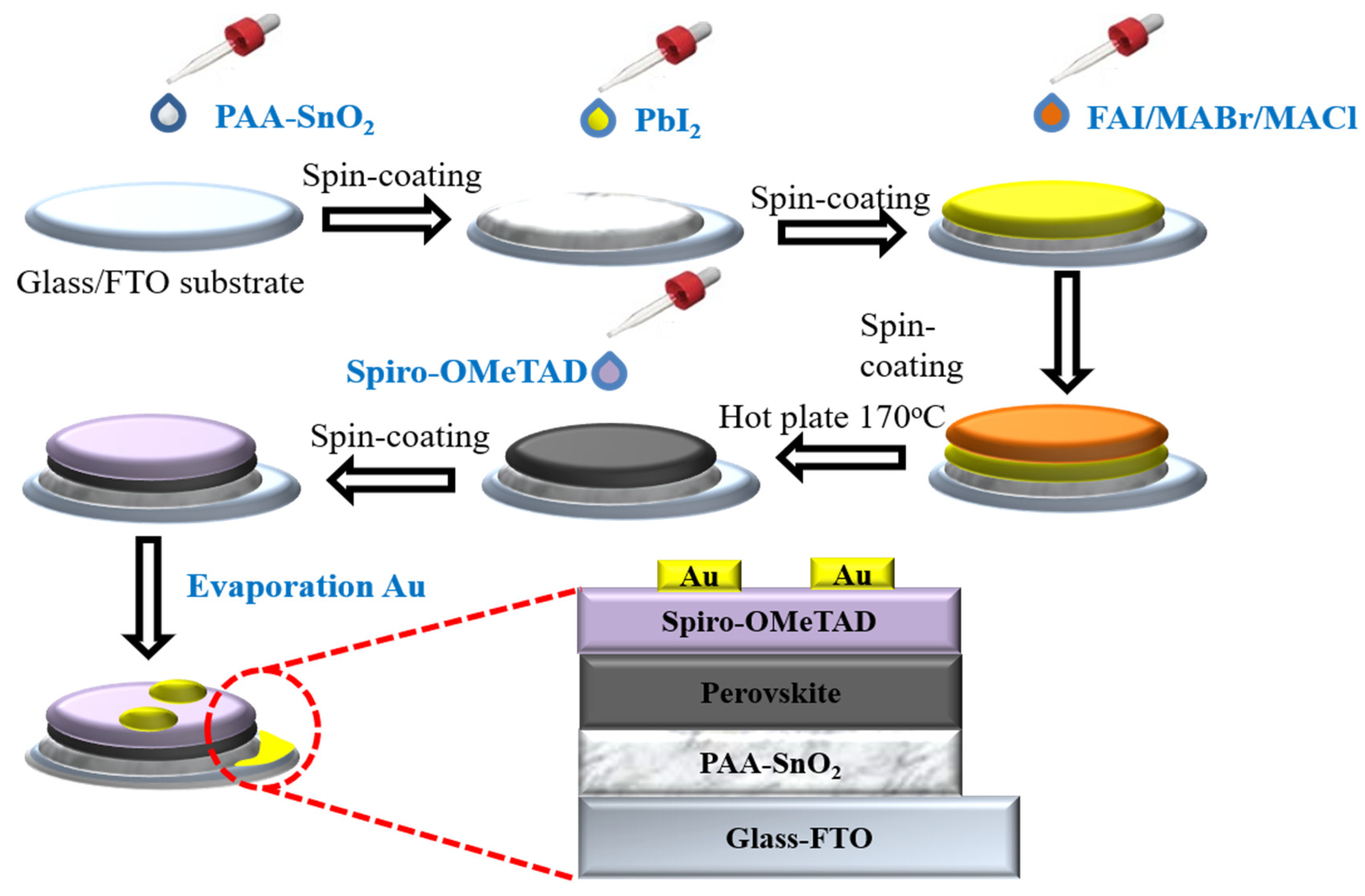
2.2. Perovskite Solar Cell Fabrication

The preparation of PSC is shown in detail in Figure 1. The glass/FTO substrate was cleaned using distilled water, acetone, and isopropanol. Then, the FTO glasses were dried using a nitrogen gun and treated with UV–ozone for 20 min. The SnO2 precursor was obtained by dissolving SnO2 (450 μL) colloid dispersion and LiCl (300 μL) aqueous solution (17 mg/4 mL) in water (2 mL) [49]. For PAA@SnO2, PAA (0.5, 1.0, 2.0, and 3.0 mg/mL) was added into the SnO2 precursor solution. The SnO2-based electron transport layer was spin-coated on the cleaned FTO at 3000 rpm for 30 s. This was followed by annealing at 150 °C for 30 min in air. Then, the substrates were treated with UV–ozone for 20 min before being transferred into a glovebox. The perovskite films were fabricated using a typical two-step sequential deposition method. First, 50 μL of PbI2 precursor solution (600 mg PbI2 dissolved in (DMF 0.9 mL) and (DMSO 0.1 mL)) was spin-coated onto SnO2 films at 2000 rpm for 20 s. The FAI/MABr/MACl mixed solution (60 mg FAI, 6 mg MABr, and 6 mg MACl dissolved in 1 mL IPA) was spin-coated onto the PbI2 film at 4000 rpm for 20 s. Then, the films were annealed at 150 °C for 20 min. After cooling to room temperature, the hole-transport layer was subsequently deposited on top of the perovskite film via spin-coating at 4000 rpm for 40 s using a chlorobenzene solution, which contained Spiro-OMeTAD (72.3 mg mL−1), tert-butylpyridine (29 μL mL−1), and bis(trifluoromethane)sulfonimide lithium salt (18.5 μL mL−1, 520 mg mL−1 in acetonitrile). Finally, 100 nm of gold electrodes were deposited on top of the devices via evaporation at approximately 10−6 Torr.

2.3. Characterization

To assess the ability of film to absorb light, the UV–Vis spectrophotometer Agilent (Varian, Cary 50, San Diego, CA, USA) was used to measure the UV–Vis light-absorption spectra of film. The X-ray diffraction (XRD) patterns were acquired using an XRD Rigaku DMAX 2200 system (Tokyo, Japan) with Cu K as the X-ray source (λ = 0.15406 nm). The Fourier transform infrared (FTIR) spectra were captured using an infrared spectrometric analyzer (Vertex 70, Bruker, Karlsruhe, Germany). Field emission scanning electron microscopy (FESEM, Hitachi S-4700, Tokyo, Japan), operating at 10 kV, was used to analyze the top and cross-sectional morphologies of the samples. Using a QuantaMaster TM 50 PTI (Piscataway, NJ, USA), steady-state photoluminescence (PL) spectra were acquired. A solar simulator (McScience K3000, Solar Simulator LAB 50, and Polaromix, Gyeonggi, Republic of Korea) simulating solar radiation with an irradiance of 100 mW cm−2 (AM 1.5 G) was used to model sunlight conditions. The external quantum efficiency (EQE) was determined using a McScience K3100 measurement system (Suwon, Republic of Korea).

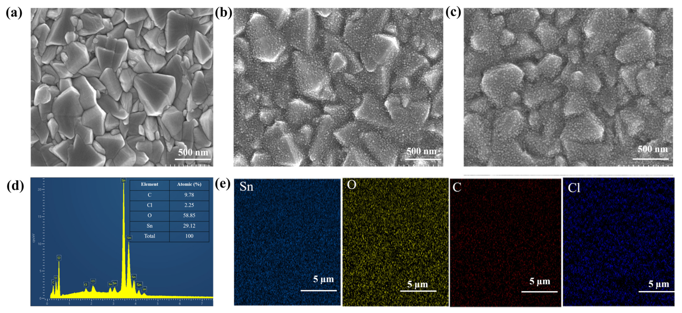
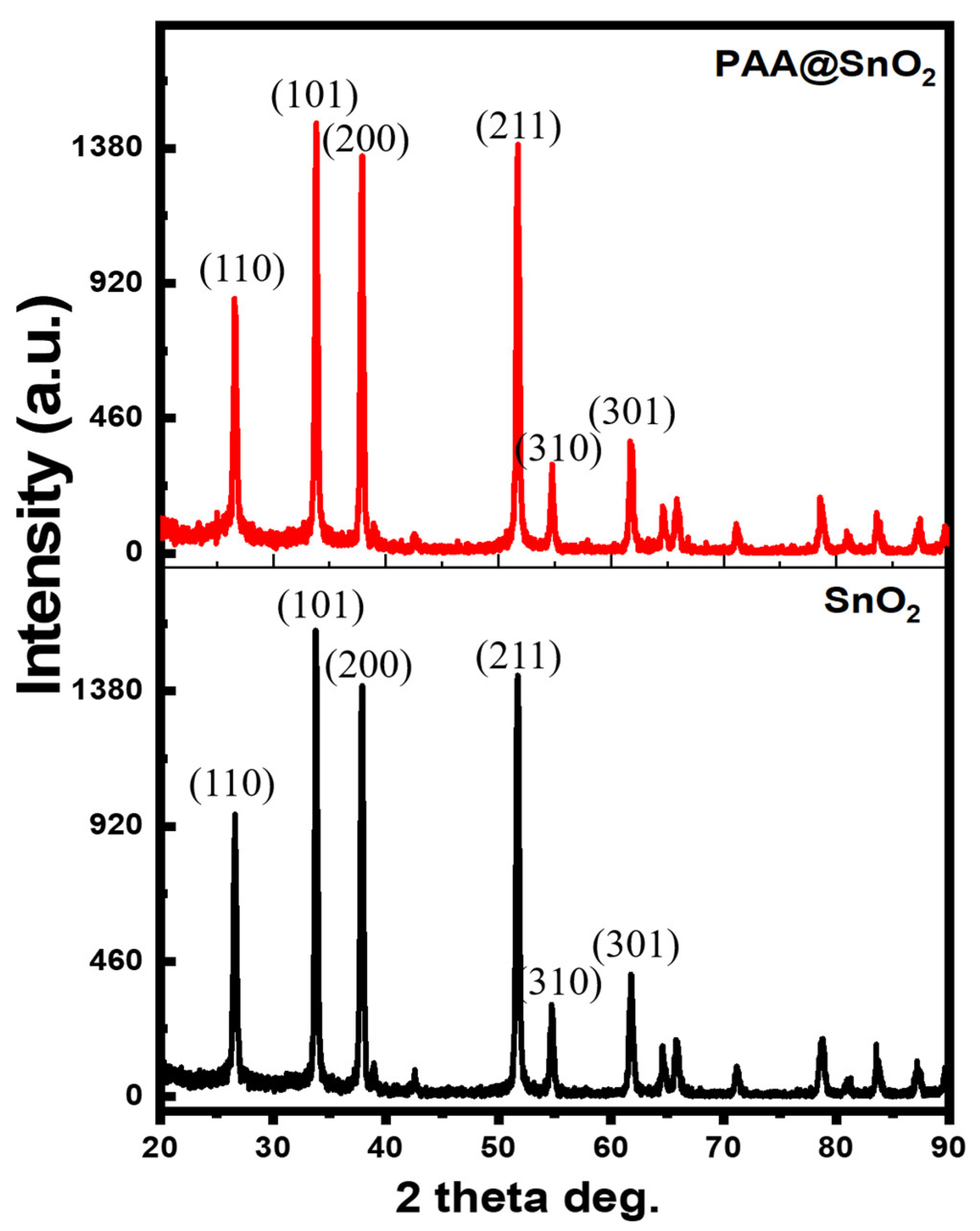
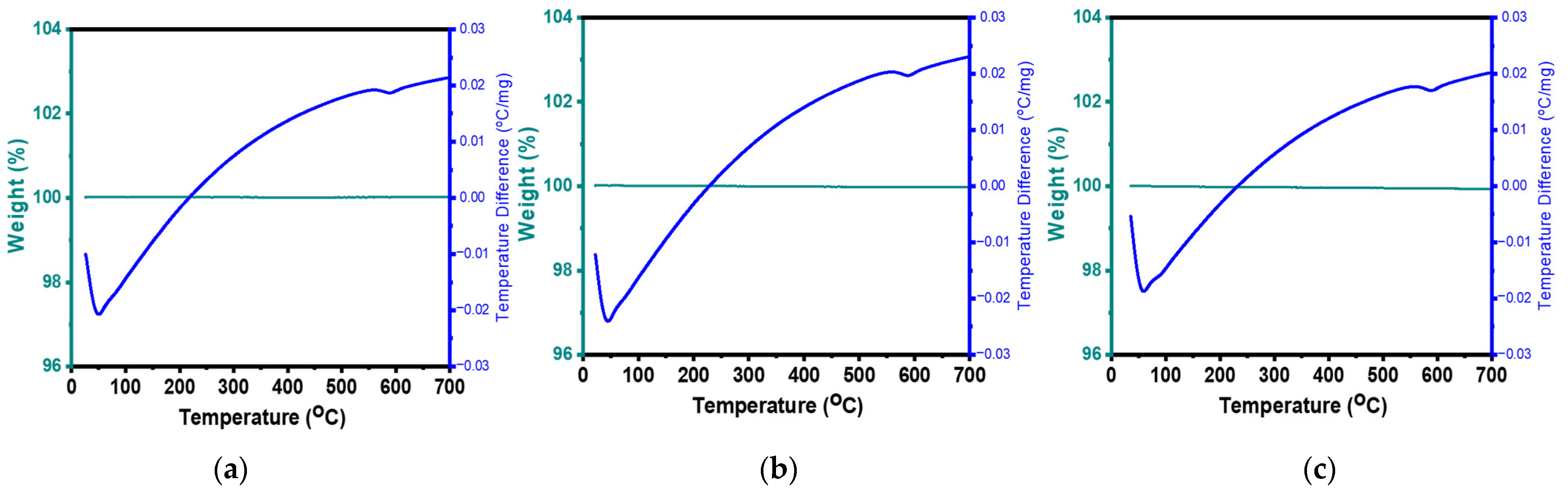
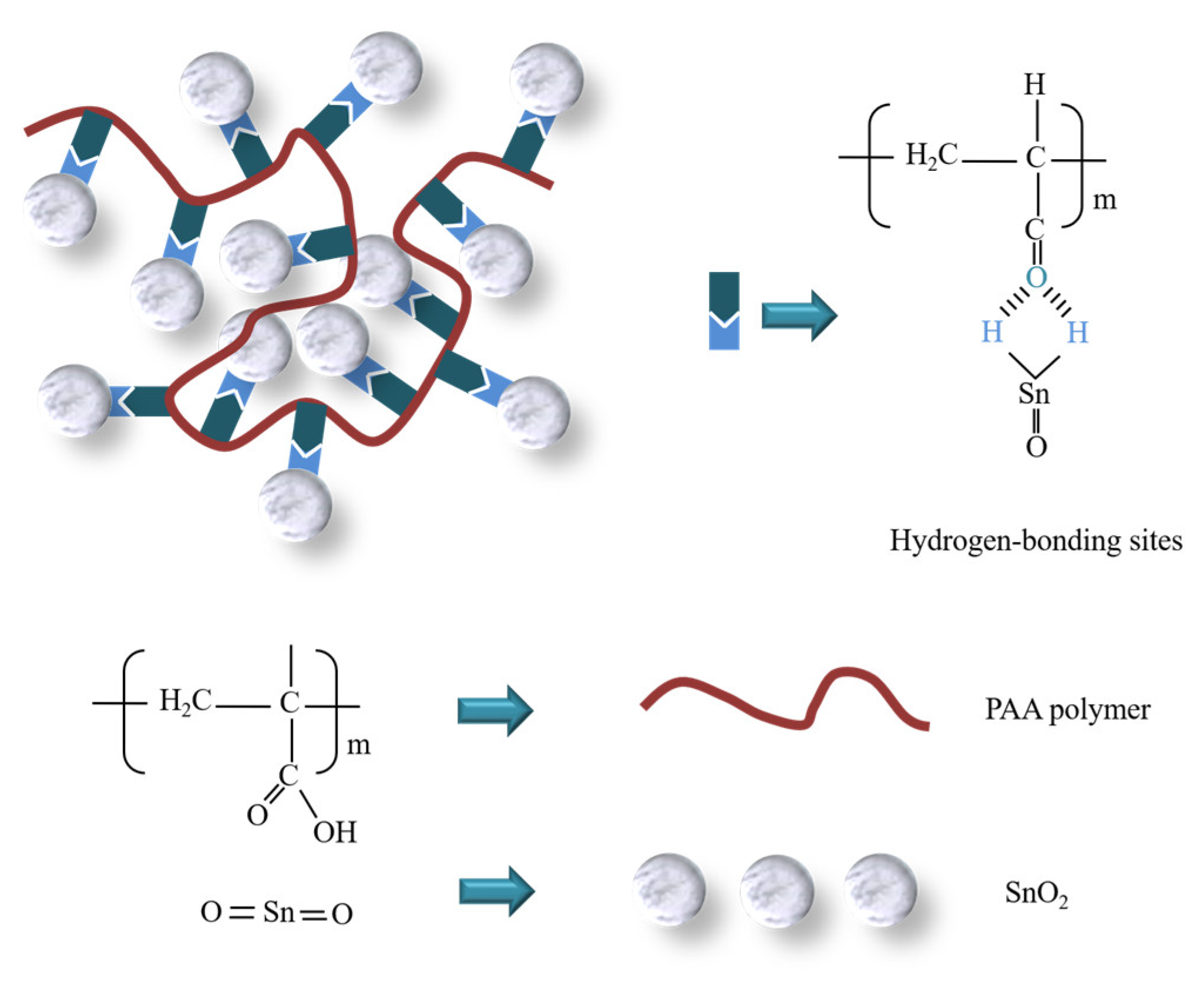
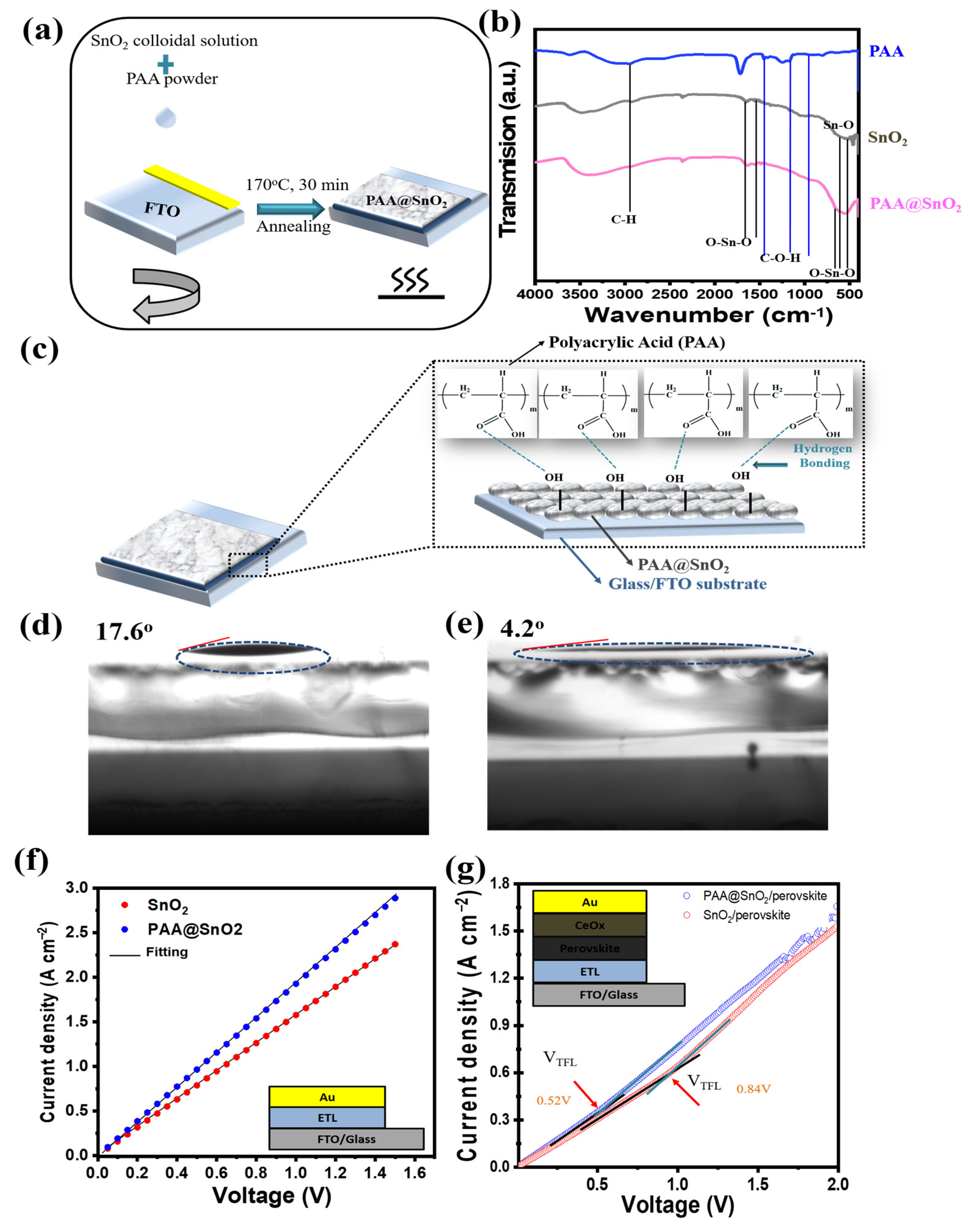
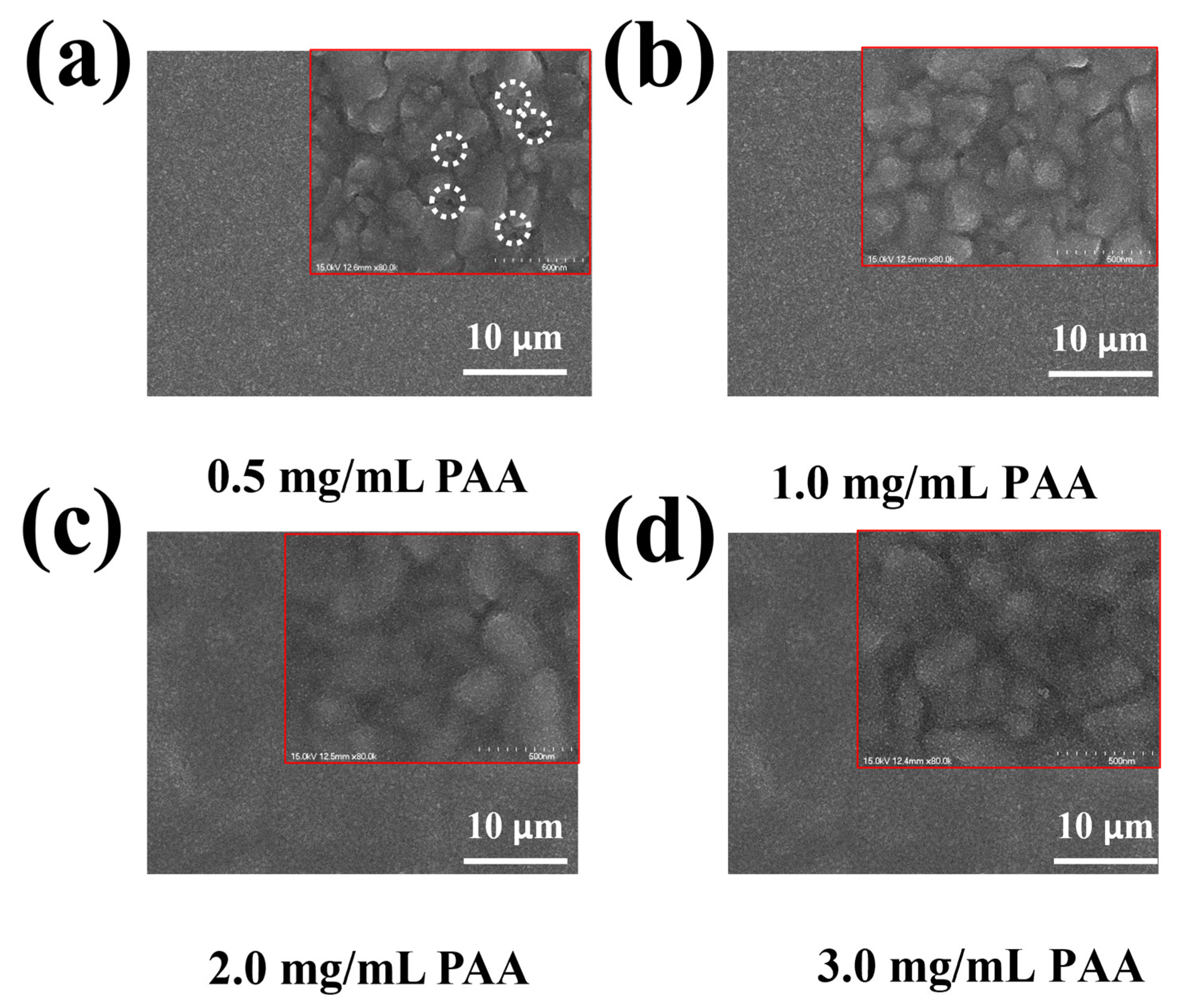
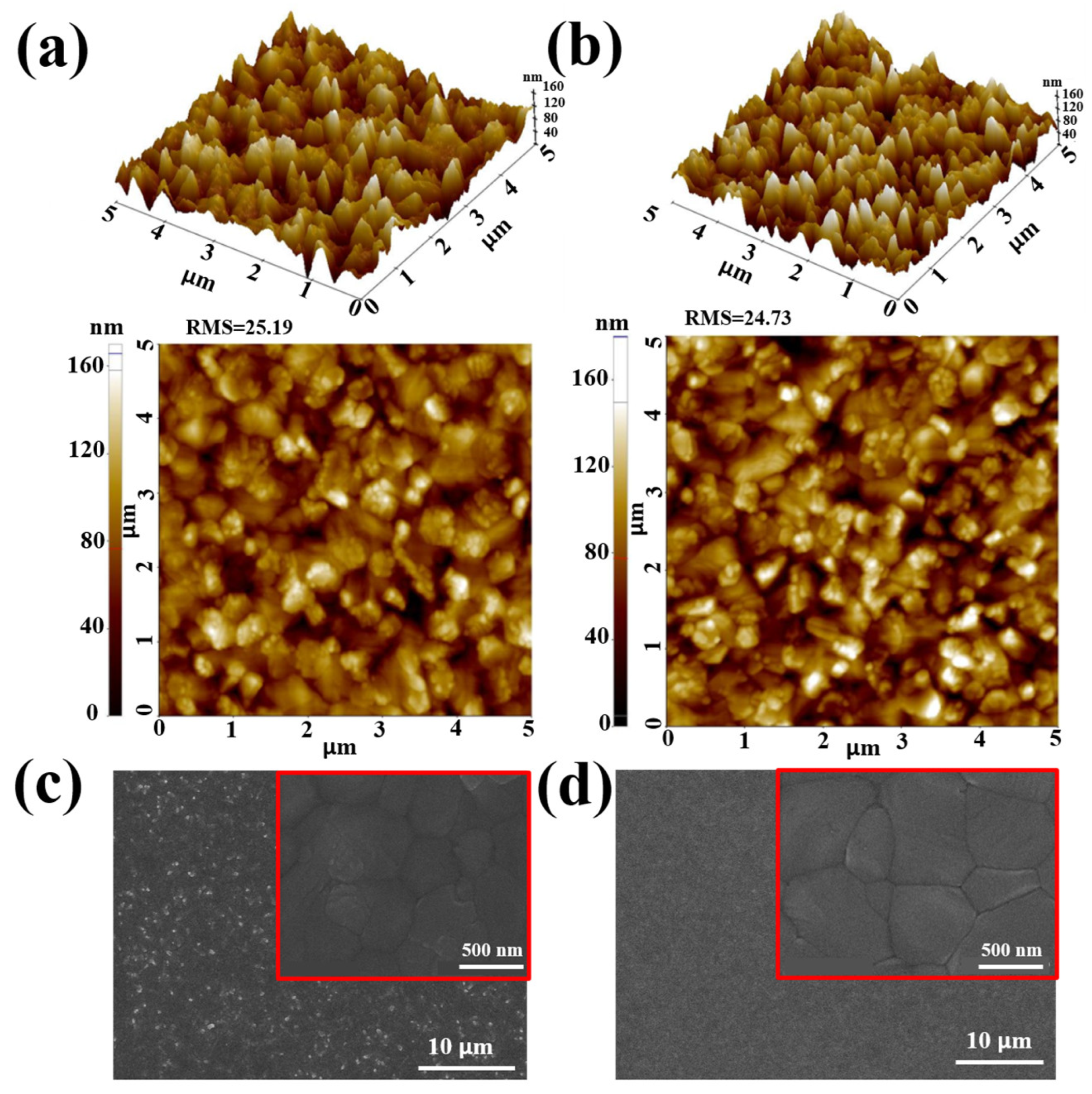
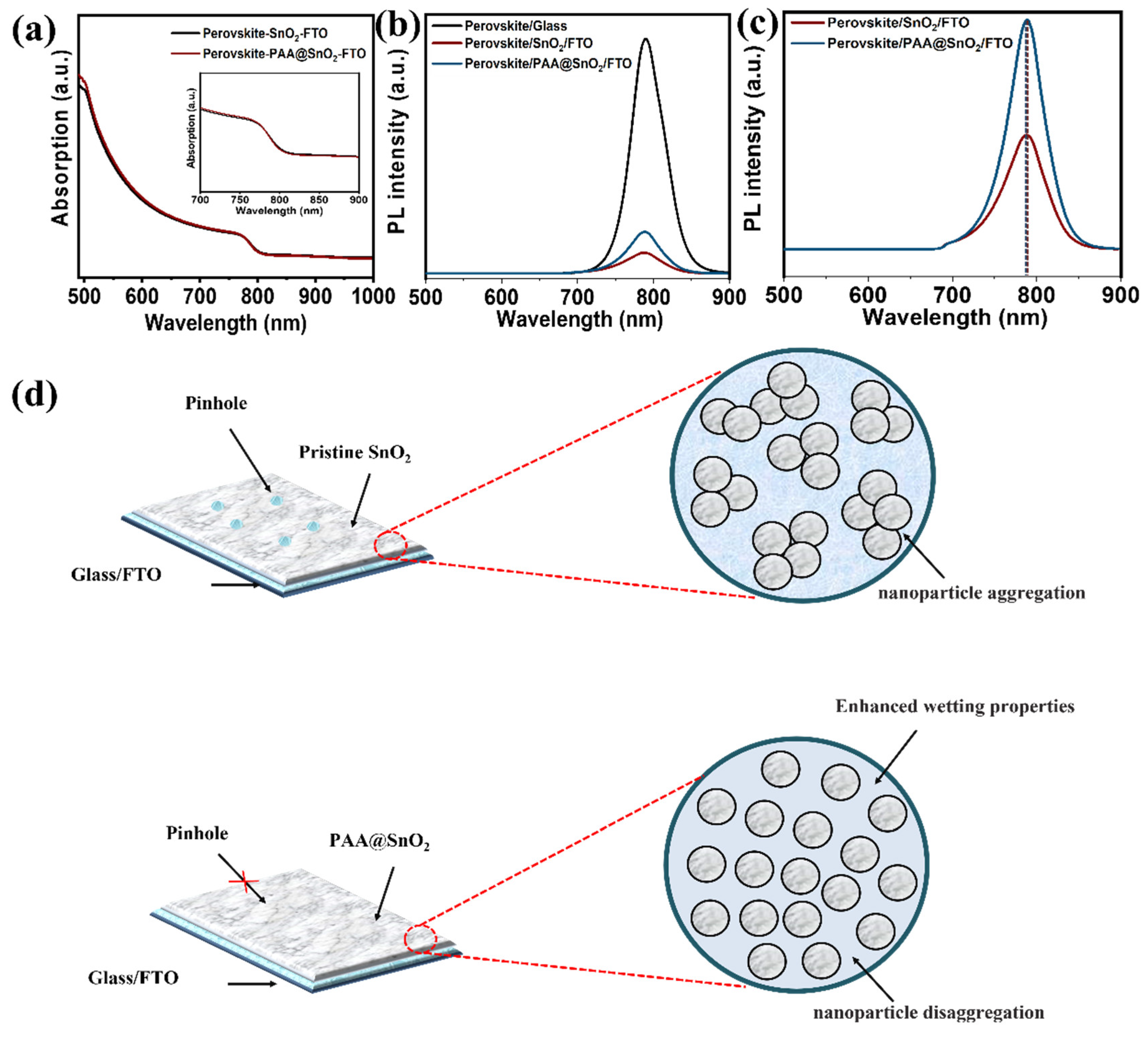
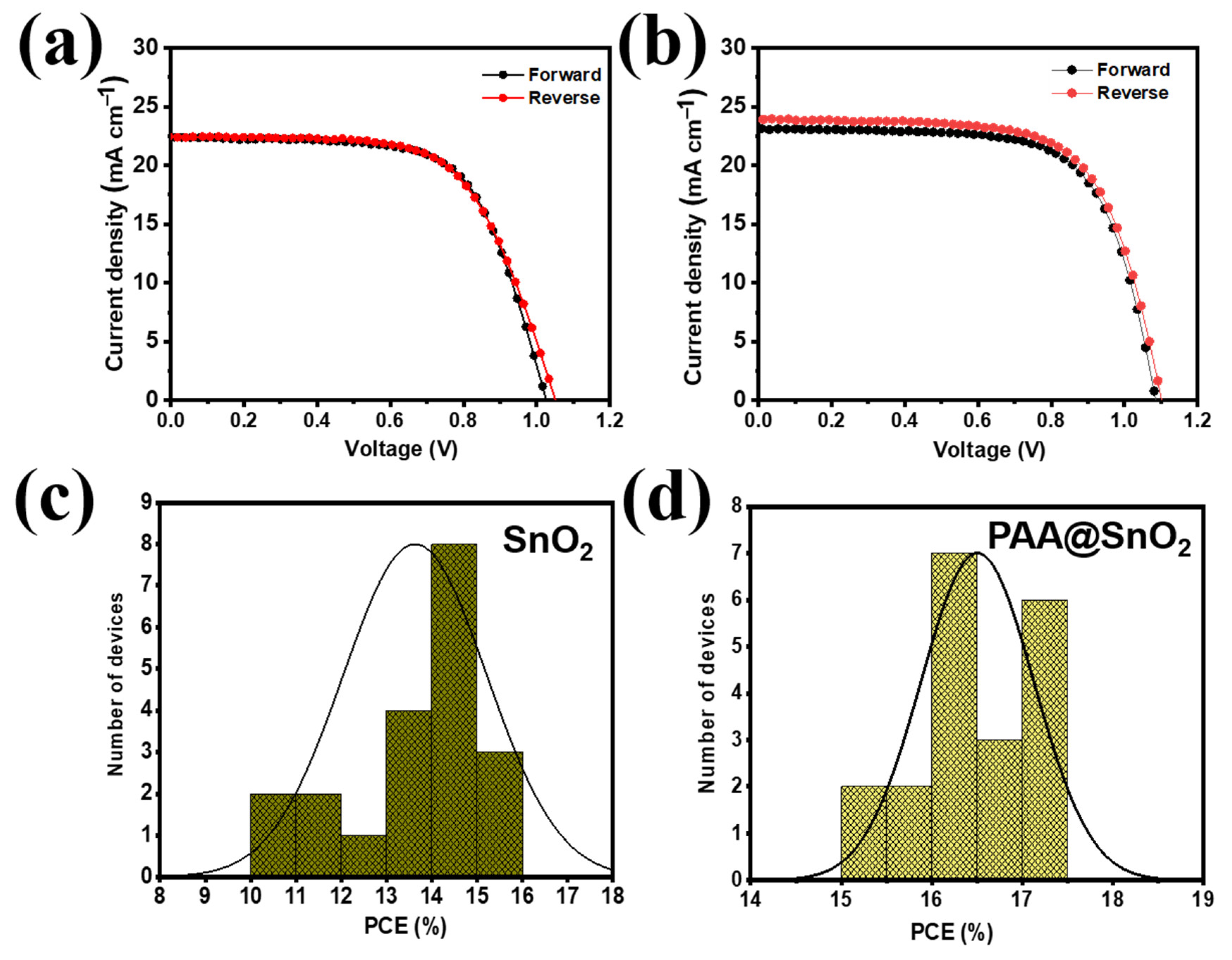
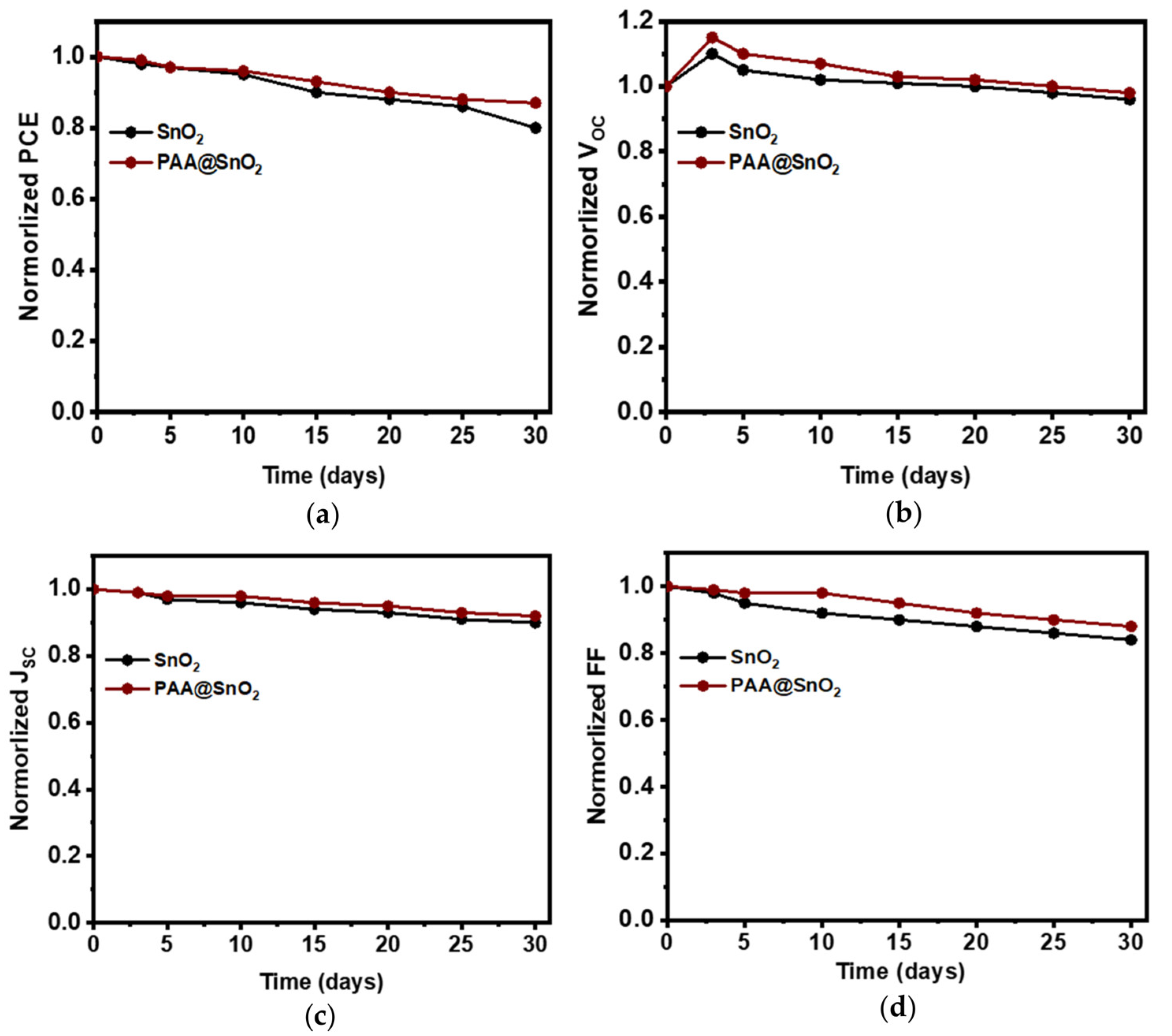
3. Results and Discussion

Despite semiconductor oxide nanoparticles being recognized as potential electron transport layer (ETL) materials for perovskite solar cells (PSCs), their tendency to agglomerate due to van der Waals forces within the colloid, coupled with their large specific surface area, presents a significant challenge [54,55]. Various strategies, including doping and surface engineering, have been implemented to curb the agglomeration of SnO2 particles in dispersion systems with small-sized particle media, thereby stabilizing SnO2 colloids. The suspension, uniformity, and stability of nanoparticles in water are heavily influenced by particle spatial agglomeration and charge balance. Introducing a suitable polymer or surfactant material helps to reduce inter-particle space and maintain a uniform charge on the particle surfaces, thus preventing oxide nanoparticle agglomeration. In this context, PAA is used as a buffering agent to stabilize SnO2 particles, working through two mechanisms: (i) PAA reduces the available active space around the particles, preventing SnO2 nanoparticle agglomeration, and (ii) crucially, functional groups on the PAA surface, when combined with SnO2 nanoparticles, help balance the charge between particles. To explore the impact of PAA on the photovoltaic characteristics and enhance PSC performance, a range of material characterization techniques were applied, as detailed throughout this manuscript.
We initially investigated the surface morphology obtained on different ETLs (SnO2 and PAA@SnO2) (as shown in Figure 2). Compared with the FTO surface (Figure 2a), SnO2 and PAA@SnO2 were successfully prepared (Figure 2b,c). However, the PAA@SnO2 nanocrystals were densely coated, and there were no pinholes on the film surface. This can prevent ineffective contact between the ETL film surface and perovskite, leading to improved optical performance. The EDX analysis presents the existing components on the PAA@SnO2 film (Figure 2d). The presence of a small amount of residual Cl (2.25%) does not significantly affect the composition of the film due to the guaranteed elemental ratio between Sn and O (specifically SnO2) along with the existence of PAA on the FTO substrate. Furthermore, Figure 2e shows the elemental mapping spectra corresponding to PAA@SnO2 film, showing the uniform distribution of Sn, O, and C nanocrystals throughout the film.
XRD analysis was performed to obtain crystallographic information regarding as-synthesised pure SnO2 and PAA@SnO2. Figure 3 displays the acquired XRD patterns for PAA@SnO2 and pristine SnO2. The main diffraction peaks at approximately 26.25°, 33.66°, 38.16°, 51.50°, 54.82°, and 61.55° for pure SnO2 correspond to (110), (101), (200), (211), (310), and (301), respectively. This indicates that a pure rutile tetragonal SnO2 structure has formed (JCPDS no. 41–1445). When a low concentration of PAA was added as a dopant, no additional peak was observed in the PAA@SnO2, indicating that PAA doping did not introduce a secondary phase as an impurity with the pure SnO2. Conversely, a reduction in peak intensity was observed in PAA@SnO2 spectrum, likely resulting from the interaction between the PAA polymer and SnO2 crystals.
Thermogravimetric analysis (TGA) and differential scanning calorimetry (DSC) were used to determine the thermal properties of FTO, FTO/SnO2, and FTO/PAA@SnO2 from 25 °C to 700 °C in nitrogen gas flowing at a rate of 10°/min. Figure 4a shows that the FTO substrate remains stable in N2 up to 700 °C. This indicates good thermal stability without pyrolysis or thermo-oxidative decay occurring. However, conducting investigations at temperatures above 700 °C is not advisable, as this can lead to a decrease in Hall mobility and reduction in the number of oxygen vacancies. These changes result in lower mobility and fewer carriers in the FTO membrane, ultimately leading to the increased resistivity of the FTO substrate [56]. Additionally, the spin-coating of SnO2 and PAA@SnO2 forms thin films of 69 and 35 nm, respectively. Thus, the mass loss is not too significant, specifically 99.98% (Figure 4b) and 99.94% (Figure 4c). Furthermore, the obtained curve of the DSC analysis is very similar. In Figure 4a–c, the DSC plot shows two endothermic peaks. The first endothermic peak is approximately in the range of 45–110 °C, corresponding to the removal of the absorbed water from the substrate [57,58]. The other small peak at 580 °C was due to further crystallinity of the FTO substrate [59,60]. Therefore, the degree of SnO2 and PAA@SnO2 crystallization on the FTO substrate is appropriate for the annealing temperature of 150 °C.
Next, to investigate the influence as well as find the optimal concentration of PAA, we adjusted the PAA concentration to 0.5, 1.0, 2.0, and 3.0 mg mL−1, respectively. The undoped or doped SnO2 ETL were spin-coated with SnO2 precursor solution at ambient temperature and then thermally annealed in air for 30 min at 170 °C. The chemical structure of PAA-SnO2 is shown in Figure 5.
Figure 6a shows a facile synthesis of ETL used to collect and transport electrons from the absorber layer to the TCO. First, the ability to transmit in the visible region of pristine SnO2 and PAA@SnO2 at different concentrations was evaluated. From Figure S1a, undoped and doped SnO2 ETL show excellent transmittance in the wavelength region from 300–900 nm, and the transmittance of the PAA@SnO2 at various film concentrations almost remains unchanged when compared with that of the pristine SnO2 film. This indicates that the addition of PAA slightly changes the optical transmittance properties of the undoped SnO2 film. Additionally, a good transmittance spectrum is advantageous to the performance of PSCs because it shows uniform film deposition with few defect states. However, a minor decrease in the transmittance of the ETL is observed, corresponding to the optical image of the solution shifting from transparent to opalescent with the increasing doping concentration of PAA, as illustrated in Figure S1b. Additionally, the absorbance progressively increases as the wavelength increases, as shown in Figure S2a. The Tauc plot (Figure S2b) was utilized to estimate the optical band edge (Eg). It was determined that the Eg of the pristine SnO2 film was 4.2 eV. This value remained nearly unchanged for PAA@SnO2, suggesting that the small amount of PAA doping did not significantly impact the Eg of the pristine SnO2 film.
Fourier transform infrared (FT-IR) spectroscopy was analyzed to determine the presence of separate components in the PAA@SnO2 film before annealing (Figure 6b). The O-Sn-O stretching mode and Sn-O vibrational mode are responsible for the absorption peaks at 550, 650, 1550, and 1690 cm−1, respectively [49]. The COOH stretching modes in PAA are responsible for the peaks to appear at 1479, 1296, and 948 cm−1. It can be seen that PAA was absorbed into SnO2 film by noting that the spectrum of PAA@SnO2 exhibits the typical peaks of SnO2 and PAA, with the O-Sn-O peaks of SnO2 shifting to 670 cm−1. Furthermore, the presence of PAA at different concentrations in the SnO2 precursor solution was demonstrated by the FT-IR spectrum (Figure S3). More importantly, we explored whether annealing plays a role in the formation of PAA@SnO2. According to Figure S4, there is a slight change in the composition of pristine SnO2 and PAA@SnO2 at various concentrations post-annealing. Notably, the presence of hydroxyl groups on the film surface at 2850 and 2915 cm−1 indicates strong hydrogen bonding with the carboxylic group in the PAA polymer. This is attributed to the high temperature of the annealing process, which promotes the partial breakdown of the Sn=O bond, leading to the formation of Sn(OH)n on the SnO2 surface. The mechanism of this hydrogen bond formation is depicted in Figure 6c. Therefore, during the annealing process, the hydroxyl group on the SnO2 surface forms a hydrogen bond with the carboxylic group of PAA (as shown in Figure 5) [49,53,61].
By suppressing the formation of large clusters in the substrate and using SnO2 that has been incorporated into PAA via hydrogen bonding, it is anticipated that the spin-coated film will become compact and uniform with a decrease in pinholes and that the PAA polymer will create a dense and compact matrix on the substrate. Additionally, to obtain complete coverage on the substrate, UV pretreatment is required because pure SnO2 film is a non-wettable surface for a perovskite precursor solution. This implies that the water contact angle measurement of pristine SnO2 is high (approximately 40°) [62,63] and clearly decreases after UV treatment (17.6°). Fortunately, PAA inclusion in SnO2 film can enhance the affinity between SnO2 and perovskite by altering the SnO2 surface, as demonstrated in Figure 6d,e and Figure S5. Therefore, increasing PAA concentration will contribute to further reducing contact angle of SnO2. However, excessively increasing the PAA concentration (specifically 3 mg/mL) will promote particle aggregation, leading to a rebound increase in contact angle data. When compared to PAA@SnO2 at various concentrations, the contact angle of the perovskite solution on pure SnO2 film was significantly higher. Additionally, perovskite is not completely coated on the virgin SnO2 substrate without pretreatment. However, perovskite on PAA@SnO2 displays a dense and compact coating (Figure S6). Hence, without any pretreatment (such as UV treatment), a complete covering of perovskite film on the PAA@SnO2 layer is accomplished.
The effect of PAA on the conductivity of the SnO2 thin films was analyzed via electrical measurements. As shown in Figure 6f, the PAA@SnO2 film exhibits a higher electron mobility (2.08 × 10⁻³ cm2 V−1 s−1) than that of the SnO2 film (8.5 × 10⁻⁴ cm2 V−1 s−1) as measured by the space charge limited current (SCLC) method [36,64]. The SCLC model was used with the electron-only devices (FTO/ETL/perovskite/CeOx/Au) to investigate the trap density [65]. The dark I-V curves for the two devices are displayed in Figure 6g. Typically, the I-V curve exhibits a linear ohmic-type response at low bias voltages. The current begins to increase nonlinearly with an increase in bias voltage, signaling the commencement of the trap-filling process. Furthermore, trap-filled limit voltage (VTFL) is the definition of the kink point that separates the linear and nonlinear regions. The trap density (Nt) can be computed using the following equation:
N t = 2   ɛ 0 ɛ   V T F L e   L 2
where ɛ0, ɛ, e, and L denote the perovskite film thickness, elementary charge, relative dielectric constant, and permittivity of vacuum, respectively. The perovskite layer on the PAA@SnO2 ETL has an estimated trap density of approximately 6.27 × 1014 cm−3, which is significantly less than the 4.4 × 1015 cm−3 of the film deposited on the SnO2 ETL, indicating that the introduction of PAA reduces the defect states of the ETL.
With or without PAA doping, compact SnO2 films were spin-coated onto FTO substrates using a colloid dispersion solution. To better understand the surface morphology of the coated films, atomic force microscopy (AFM) was employed. Given that FTO shows a roughness surface of 30 nm [66,67], both SnO2 ETL films exhibit a smooth surface, as observed in Figure S7a,b. However, a pristine SnO2 film exhibits a rougher surface than the SnO2 ETL films (26.32 nm vs. 24.98 nm), which is in line with the surface morphology observed via scanning electron microscopy (SEM), as shown in Figure 2b,c. Furthermore, it should be observed that at a concentration of 0.5 mg mL−1, several pinholes are visible, despite the fact that the agglomeration between particles is significantly reduced when compared to pristine SnO2 (as shown in Figure 7a). This result suggests that the SnO2 oligomers can be disaggregated by the hydrogen bonds of PAA and SnO2 particles. However, their affinity is insufficient to glue the particles together. When the concentration increases slightly (1.0 mg mL−1), the PAA@SnO2 surface is pinhole-free with no intergranular agglomeration through uniform particle formation (Figure 7b). Additionally, due to the high hydrogen bonding affinity between PAA and SnO2, which occurred when the mass concentration of PAA exceeded 1.0 mg mL−1 or when there were more PAA components present, PAA@SnO2 aggregated into large particles and failed to form a uniform and dense ETL layer in Figure 7c–d.
AFM measurements revealed that the root mean square (RMS) roughnesses of perovskite films on SnO2 and PAA@SnO2 were 25.19 nm and 24.73 nm, respectively. This smoother perovskite is shown in Figure 8a,b. The SEM images of the absorber layer deposited onto various ETLs are shown in Figure 8c,d. The images confirm the surface morphology of the perovskite layers. The perovskite coated on PAA@SnO2 was also discovered to be bigger than that coated on the SnO2 layers. Additionally, as shown in Figure S8, the effects of various PAA concentrations in a SnO2 colloidal solution on the surface morphology of perovskite layers were also obtained. It can be determined that the crystal grains of the perovskite on PAA@SnO2 (0.5 and 1.0 mg/mL) are more uniform with less white PbI2 phase in comparison with those of the perovskite on pristine SnO2 and PAA@SnO2 (2.0 and 3.0 mg/mL). The result indicates that PAA@SnO2 can facilitate a uniform distribution of nucleation sites. Given that the incorporation of PAA leads to reduced roughness in the ETL thin film, the presence of a pre-existing functional group (carboxylic acid) on the PAA surface readily bonds with SnO2 to form hydrogen bonding, leading to nanoparticle disaggregation as well as the enhanced wetting properties of ETL for perovskite precursor solution.
By adjusting the PAA concentration and layer thickness, the performance of the device is maximized. To successfully enable electron transport for ETL, the concentration of insulating PAA in SnO2 should be maintained to a minimum. According to Table S1, the PCE of devices increases as PAA concentration increases, and the fill factor achieves its maximum when PAA content reaches 1.0 mg mL−1. Conversely, there was a decrease in device PCE as the concentration of PAA increased (e.g., 2.0 and 3.0 mg mL−1), which is thought to decrease the presence of SnO2 nanoparticles in solution. Furthermore, the high affinity between PAA and SnO2 contributes significantly to the formation of nanoparticle aggregations. Additionally, due to the weak conductivity of SnO2 produced at low temperatures, the layer thickness should be as thin as possible while still preventing significant current leakage. For both pure SnO2 and PAA@SnO2, a well-defined boundary between each layer indicates thick coatings on the substrate, as shown in Figure S9a,b. Notably, the PAA@SnO2 layer is significantly thinner (approximately 35 nm) when compared to pure SnO2 (approximately 69 nm). The polymer matrix reduces the thickness of the ETL by approximately 50%, a substantial reduction when compared to the majority of ETLs reported in literature [68,69], which can enhance ETL light transmission and decrease series resistance. Furthermore, the thicknesses of the perovskite, spiro-OMeTAD, and metal electrode (Au) layers are approximately 560 nm, 195 nm, and 30 nm, respectively. Additionally, cross-section SEM images show that the surface roughness of pristine SnO2 is higher than that of PAA@SnO2 (Figure S9c,d). This highlights the advantages of using polymer doping materials, especially those with functional groups on their surfaces, such as PAA in this study.
UV–Vis spectroscopy was used to assess the light-harvesting capabilities of perovskites with varied SnO2 and PAA@SnO2 ETLs (Figure 9a). Evidently, the PAA@SnO2 layer has a minor impact on the perovskite layer’s capacity for absorption. Nevertheless, its bandgap has not changed. From the Tauc plot in Figure S10, the value of Eg is estimated to be 2.05 eV, and there is not much difference in Eg between PAA@SnO2 and pristine SnO2. Therefore, doping PAA does not significantly affect the pristine SnO2 structure for the formation of the perovskite layer. Figure 9b,c show the steady-state photoluminescence (PL) of the absorber produced on different films. The PL peaks of the perovskite on SnO2 and PAA@SnO2 can be shown to have been significantly quenched, demonstrating a perfect band-edge alignment of SnO2 with perovskite (Figure 9b). The PL intensity of the perovskite film on the surface of the PAA@SnO2 film is greater than that observed on the SnO2 film under the identical test conditions. The perovskite layer on PAA@SnO2 may have undergone less nonradiative recombination due to the stronger PL intensity [70,71,72,73]. Additionally, the perovskite film’s PL peak on the PAA@SnO2 ETL shifts by around 1.1 nm to a lower wavelength, which signals fewer defects (Figure 9c) [74]. Using PAA-incorporated SnO2, the performance of PSC will be increased for two reasons, according to an examination of the characteristics of PAA@SnO2 when compared to virgin SnO2 (Figure 9d). First, pinholes can be minimized for film thicknesses under 40 nm by inhibiting nanoparticle aggregation, resulting in a more compact and homogeneous surface. Second, the PAA polymer can enhance the substrate’s wetting properties.
Based on the aforementioned advantages, the photovoltaic properties of undoped and doped-based SnO2 PSCs were evaluated. The J−V curves for SnO2 and PAA@SnO2-based devices in the reverse and forward scan directions are shown in Figure 10a,b and Figure S11. Table 2 illustrates the PAA@SnO2-based devices with high efficiency and J−V characteristics of the champion devices using ETLs. The devices based on the SnO2 ETL substrate exhibit a maximum PCE of 15.7%, with the specific values of Voc = 1.06 V, Jsc = 22.39 mA cm−2, and FF = 0.68. Surprisingly, by switching the control ETL to a PAA@SnO2 ETL, the detailed parameters of Voc and FF were considerably enhanced to 1.08 V and 0.73%, respectively. Furthermore, the optimal PCE can be increased to 17.2%. This study shows that interfacial carrier recombination was significantly reduced by the PAA@SnO2 layer’s ability to passivate charge recombination at the ETL/perovskite interfaces. For each undoped and PAA-doped ETL, we created 20 different devices to test the repeatability of the material and technique, as shown in Table S2. The distribution of device parameters is shown in Figure 10c,d together with the statistical parameters that are presented in Figure S12. The J–V values for the doped SnO2-based devices clearly show a narrow distribution with a low standard deviation, indicating exceptional repeatability.
The long-term stability of PSCs with SnO2 and PAA@SnO2 was evaluated in a nitrogen environment without encapsulation. Figure 11 illustrates the shelf stability of PSCs with different ETLs over time. After 30 days of storage, the device using the PAA@SnO2 ETL retained 89% of its original power conversion efficiency (PCE), whereas the device with the SnO2 ETL experienced a 21% reduction in its initial PCE. This indicates that devices with the PAA@SnO2 ETL are more stable, likely due to improved contact between the PAA@SnO2 ETL and perovskite layer. The degradation of the charge carrier transport layer and perovskite layer is a well-known factor contributing to the instability of PSCs. The enhanced stability in the PAA@SnO2-based devices when compared to those with SnO2 can be attributed to the improved interaction between the ETL and the perovskite layer.
Table 3 summarizes the performance of PSCs with different doping materials in SnO2 ETL. When compared to the performance of other recent PSCs, our PAA@SnO2 exhibits performance increases from 15.7% to 17.2% (increase of approximately 10% in performance). It can be observed that doping with organic materials, specifically polymers, is slightly more effective than doping with inorganic materials due to the large particle size of the material, which easily forms large clusters on the ETL surface, contributing to reducing the surface contact between ETL and perovskite.

4. Conclusions

In summary, a straightforward and cost-effective technique has been suggested for the incorporation of PAA into the SnO2 matrix to create a high-quality electron-selective layer. The PAA@SnO2 layer, characterized by its dense and uniform structure with an ultra-thin thickness below 40 nm, is attributed to the enhanced dispersibility of the SnO2 substrate. Due to the enhanced wetting properties of the polymer-modified film, a pinhole-free and high-quality perovskite film is easily formed on the PAA@SnO2 matrix. Effective PSCs based on the PAA@SnO2 matrix have been demonstrated, achieving a power conversion efficiency of 17.2% with high repeatability and shelf stability. This study presents a novel perspective on the inclusion of polymers as electron/hole selective layers in colloidal quantum dot inks. It is anticipated that future research and development involving other inorganic nanoparticle inks combined with suitable polymers will enhance device performance. This study highlights a new approach in the simple combination of polymers with metal oxides, acting as an effective electron/hole selective layer. The development of different polymers with suitable metal oxides is expected to further improve the current performance of devices. This process is promising in its simplicity and effectiveness, promoting its potential widespread application on an industrial scale.

Supplementary Materials

The following supporting information can be downloaded at: https://www.mdpi.com/article/10.3390/polym16020199/s1.

Author Contributions

Investigation, V.P.H.H.; data curation, V.P.H.H.; writing—original draft preparation, V.P.H.H.; conceptualization, C.-W.B.; methodology, C.-W.B.; writing—review and editing, C.-W.B.; supervision, C.-W.B.; funding acquisition, C.-W.B. All authors have read and agreed to the published version of the manuscript.

Funding

This research was funded by the National Research Foundation of Korea (NRF) funded by the Ministry of Science and ICT (NRF-2020R1F1A1076576) and by the Korea Basic Science Institute grant funded by the Ministry of Education (2019R1A6C1010016). Furthermore, this study was supported by the Korea Institute of Energy Technology Evaluation and Planning (KETEP) and the Ministry of Trade, Industry, and Energy (MOTIE) of the Republic of Korea (no. 1415188041).

Data Availability Statement

Data are contained within the article and supplementary materials.

Acknowledgments

This study was supported by grants from the National Research Foundation of Korea (NRF) funded by the Ministry of Science and ICT (NRF-2020R1F1A1076576) and by the Korea Basic Science Institute grant funded by the Ministry of Education (2019R1A6C1010016). Furthermore, this study was supported by the Korea Institute of Energy Technology Evaluation and Planning (KETEP) and the Ministry of Trade, Industry, and Energy (MOTIE) of the Republic of Korea (no. 1415188041).

Conflicts of Interest

The authors declare that they have no known competing financial interests or personal relationships that could have appeared to influence the work reported in this paper.

References

  1. Miyata, A.; Mitioglu, A.; Plochocka, P.; Portugall, O.; Wang, J.T.-W.; Stranks, S.D.; Snaith, H.J.; Nicholas, R.J. Direct measurement of the exciton binding energy and effective masses for charge carriers in organic–inorganic tri-halide perovskites. Nat. Phys. 2015, 11, 582–587. [Google Scholar] [CrossRef]
  2. Snaith, H.J. Perovskites: The Emergence of a New Era for Low-Cost, High-Efficiency Solar Cells. J. Phys. Chem. Lett. 2013, 4, 3623–3630. [Google Scholar] [CrossRef]
  3. Jung, H.S.; Park, N. Perovskite Solar Cells: From Materials to Devices. Small 2015, 11, 10–25. [Google Scholar] [CrossRef]
  4. Yang, L.; Barrows, A.T.; Lidzey, D.G.; Wang, T. Recent progress and challenges of organometal halide perovskite solar cells. Rep. Prog. Phys. 2016, 79, 026501. [Google Scholar] [CrossRef]
  5. Park, J.; Kim, J.; Yun, H.-S.; Paik, M.J.; Noh, E.; Mun, H.J.; Kim, M.G.; Shin, T.J.; Seok, S.I. Controlled growth of perovskite layers with volatile alkylammonium chlorides. Nature 2023, 616, 724–730. [Google Scholar] [CrossRef]
  6. Ma, F.; Zhao, Y.; Qu, Z.; You, J. Developments of Highly Efficient Perovskite Solar Cells. Accounts Mater. Res. 2023, 4, 716–725. [Google Scholar] [CrossRef]
  7. Tiwari, S.K.; Shankar, G.; Kumar, P.; Laref, A.; Pradhan, B. Efficiency Approaching 26% in Triple Cation Mixed Halide Perovskite Solar Cells by Numerical Simulation. IEEE J. Photovolt. 2023, 13, 242–249. [Google Scholar] [CrossRef]
  8. Yoshikawa, K.; Kawasaki, H.; Yoshida, W.; Irie, T.; Konishi, K.; Nakano, K.; Uto, T.; Adachi, D.; Kanematsu, M.; Uzu, H.; et al. Silicon heterojunction solar cell with interdigitated back contacts for a photoconversion efficiency over 26%. Nat. Energy 2017, 2, 17032. [Google Scholar] [CrossRef]
  9. Bush, K.A.; Bailie, C.D.; Chen, Y.; Bowring, A.R.; Wang, W.; Ma, W.; Leijtens, T.; Moghadam, F.; McGehee, M.D. Thermal and Environmental Stability of Semi-Transparent Perovskite Solar Cells for Tandems Enabled by a Solution-Processed Nanoparticle Buffer Layer and Sputtered ITO Electrode. Adv. Mater. 2016, 28, 3937–3943. [Google Scholar] [CrossRef]
  10. Grätzel, M. The Rise of Highly Efficient and Stable Perovskite Solar Cells. Accounts Chem. Res. 2017, 50, 487–491. [Google Scholar] [CrossRef]
  11. Ono, L.K.; Park, N.-G.; Zhu, K.; Huang, W.; Qi, Y. Perovskite Solar Cells—Towards Commercialization. ACS Energy Lett. 2017, 2, 1749–1751. [Google Scholar] [CrossRef]
  12. Wang, Y.; Li, S.; Zhang, P.; Liu, D.; Gu, X.; Sarvari, H.; Ye, Z.; Wu, J.; Wang, Z.; Chen, Z.D. Solvent annealing of PbI2for the high-quality crystallization of perovskite films for solar cells with efficiencies exceeding 18%. Nanoscale 2016, 8, 19654–19661. [Google Scholar] [CrossRef]
  13. Domanski, K.; Alharbi, E.A.; Hagfeldt, A.; Grätzel, M.; Tress, W. Systematic investigation of the impact of operation conditions on the degradation behaviour of perovskite solar cells. Nat. Energy 2018, 3, 61–67. [Google Scholar] [CrossRef]
  14. Snaith, H.J.; Abate, A.; Ball, J.M.; Eperon, G.E.; Leijtens, T.; Noel, N.K.; Stranks, S.D.; Wang, J.T.-W.; Wojciechowski, K.; Zhang, W. Anomalous Hysteresis in Perovskite Solar Cells. J. Phys. Chem. Lett. 2014, 5, 1511–1515. [Google Scholar] [CrossRef]
  15. Wei, J.; Li, H.; Zhao, Y.; Zhou, W.; Fu, R.; Leprince-Wang, Y.; Yu, D.; Zhao, Q. Suppressed hysteresis and improved stability in perovskite solar cells with conductive organic network. Nano Energy 2016, 26, 139–147. [Google Scholar] [CrossRef]
  16. Zhao, Y.; Zhou, W.; Ma, W.; Meng, S.; Li, H.; Wei, J.; Fu, R.; Liu, K.; Yu, D.; Zhao, Q. Correlations between Immobilizing Ions and Suppressing Hysteresis in Perovskite Solar Cells. ACS Energy Lett. 2016, 1, 266–272. [Google Scholar] [CrossRef]
  17. Wei, J.; Shi, C.; Zhao, Y.; Zhou, W.; Li, H.; Fu, R.; Yu, D.; Zhao, Q. Potentials and challenges towards application of perovskite solar cells. Sci. China Mater. 2016, 59, 769–778. [Google Scholar] [CrossRef]
  18. Shao, Y.; Xiao, Z.; Bi, C.; Yuan, Y.; Huang, J. Origin and elimination of photocurrent hysteresis by fullerene passivation in CH3NH3PbI3 planar heterojunction solar cells. Nat. Commun. 2014, 5, 5784. [Google Scholar] [CrossRef]
  19. Nie, W.; Tsai, H.; Blancon, J.; Liu, F.; Stoumpos, C.C.; Traore, B.; Kepenekian, M.; Durand, O.; Katan, C.; Tretiak, S.; et al. Critical Role of Interface and Crystallinity on the Performance and Photostability of Perovskite Solar Cell on Nickel Oxide. Adv. Mater. 2018, 30, 1703879. [Google Scholar] [CrossRef]
  20. Wang, Y.; Wan, J.; Ding, J.; Hu, J.; Wang, D. A Rutile TiO2 Electron Transport Layer for the Enhancement of Charge Collection for Efficient Perovskite Solar Cells. Angew. Chem. Int. Ed. 2019, 58, 9414–9418. [Google Scholar] [CrossRef] [PubMed]
  21. Wang, J.; Pan, H.; Xu, X.; Jin, H.; Ma, W.; Xiong, S.; Bao, Q.; Tang, Z.; Ma, Z. Li-Doped ZnO Electron Transport Layer for Improved Performance and Photostability of Organic Solar Cells. ACS Appl. Mater. Interfaces 2022, 14, 12450–12460. [Google Scholar] [CrossRef] [PubMed]
  22. Jiang, J.; Lang, X.; Zeng, Q.; Faheem, M.B.; Rong, S.; Zhao, H.; Li, Y. Polyacetylene derivatives in perovskite solar cells: From defect passivation to moisture endurance. J. Mater. Chem. A 2021, 9, 13220–13230. [Google Scholar] [CrossRef]
  23. Liu, X.; Chueh, C.-C.; Zhu, Z.; Jo, S.B.; Sun, Y.; Jen, A.K.-Y. Highly crystalline Zn2SnO4 nanoparticles as efficient electron-transporting layers toward stable inverted and flexible conventional perovskite solar cells. J. Mater. Chem. A 2016, 4, 15294–15301. [Google Scholar] [CrossRef]
  24. Hu, W.; Liu, T.; Yin, X.; Liu, H.; Zhao, X.; Luo, S.; Guo, Y.; Yao, Z.; Wang, J.; Wang, N.; et al. Hematite electron-transporting layers for environmentally stable planar perovskite solar cells with enhanced energy conversion and lower hysteresis. J. Mater. Chem. A 2017, 5, 1434–1441. [Google Scholar] [CrossRef]
  25. Zhang, X.; Li, J.; Bi, Z.; He, K.; Xu, X.; Xiao, X.; Zhu, Y.; Zhan, Y.; Zhong, L.; Xu, G.; et al. Stable and efficient air-processed perovskite solar cells employing low-temperature processed compact In2O3 thin films as electron transport materials. J. Alloys Compd. 2020, 836, 155460. [Google Scholar] [CrossRef]
  26. Mo, Y.; Wang, C.; Zheng, X.; Zhou, P.; Li, J.; Yu, X.; Yang, K.; Deng, X.; Park, H.; Huang, F.; et al. Nitrogen-doped tin oxide electron transport layer for stable perovskite solar cells with efficiency over 23%. Interdiscip. Mater. 2022, 1, 309–315. [Google Scholar] [CrossRef]
  27. Tan, H.; Jain, A.; Voznyy, O.; Lan, X.; de Arquer, F.P.G.; Fan, J.Z.; Quintero-Bermudez, R.; Yuan, M.; Zhang, B.; Zhao, Y.; et al. Efficient and stable solution-processed planar perovskite solar cells via contact passivation. Science 2017, 355, 722–726. [Google Scholar] [CrossRef] [PubMed]
  28. Tress, W.; Marinova, N.; Moehl, T.; Zakeeruddin, S.M.; Nazeeruddin, M.K.; Grätzel, M. Understanding the rate-dependent J–V hysteresis, slow time component, and aging in CH3NH3PbI3 perovskite solar cells: The role of a compensated electric field. Energy Environ. Sci. 2015, 8, 995–1004. [Google Scholar] [CrossRef]
  29. Zhang, M.; Yan, K.; Han, W.; Yang, S. One-pot Synthesis of Mesoporous TiO2 from Self-Assembled Sol Particles and Its Application as Mesoscopic Photoanodes of Dye-Sensitized Solar Cells. Chempluschem 2013, 78, 647–655. [Google Scholar] [CrossRef]
  30. Yang, D.; Zhou, X.; Yang, R.; Yang, Z.; Yu, W.; Wang, X.; Li, C.; Liu, S.; Chang, R.P.H. Surface optimization to eliminate hysteresis for record efficiency planar perovskite solar cells. Energy Environ. Sci. 2016, 9, 3071–3078. [Google Scholar] [CrossRef]
  31. Son, D.-Y.; Lee, J.-W.; Choi, Y.J.; Jang, I.-H.; Lee, S.; Yoo, P.J.; Shin, H.; Ahn, N.; Choi, M.; Kim, D.; et al. Self-formed grain boundary healing layer for highly efficient CH3NH3PbI3 perovskite solar cells. Nat. Energy 2016, 1, 16081. [Google Scholar] [CrossRef]
  32. Shin, S.S.; Yeom, E.J.; Yang, W.S.; Hur, S.; Kim, M.G.; Im, J.; Seo, J.; Noh, J.H.; Seok, S.I. Colloidally prepared La-doped BaSnO3 electrodes for efficient, photostable perovskite solar cells. Science 2017, 356, 167–171. [Google Scholar] [CrossRef] [PubMed]
  33. Luo, J.; Chen, J.; Wu, B.; Goh, T.W.; Qiao, W.; Ku, Z.; Bin Yang, H.; Zhang, L.; Sum, T.C.; Liu, B. Surface Rutilization of Anatase TiO2 for Efficient Electron Extraction and Stable Pmax Output of Perovskite Solar Cells. Chem 2018, 4, 911–923. [Google Scholar] [CrossRef]
  34. Yang, D.; Yang, R.; Wang, K.; Wu, C.; Zhu, X.; Feng, J.; Ren, X.; Fang, G.; Priya, S.; Liu, S. High efficiency planar-type perovskite solar cells with negligible hysteresis using EDTA-complexed SnO2. Nat. Commun. 2018, 9, 3239. [Google Scholar] [CrossRef] [PubMed]
  35. Jiang, Q.; Chu, Z.; Wang, P.; Yang, X.; Liu, H.; Wang, Y.; Yin, Z.; Wu, J.; Zhang, X.; You, J. Planar-Structure Perovskite Solar Cells with Efficiency beyond 21%. Adv. Mater. 2017, 29, 1703852. [Google Scholar] [CrossRef] [PubMed]
  36. Jiang, Q.; Zhang, L.; Wang, H.; Yang, X.; Meng, J.; Liu, H.; Yin, Z.; Wu, J.; Zhang, X.; You, J. Enhanced electron extraction using SnO2 for high-efficiency planar-structure HC(NH2)2PbI3-based perovskite solar cells. Nat. Energy 2016, 2, 16177. [Google Scholar] [CrossRef]
  37. Wu, W.; Chen, D.; Cheng, Y.; Caruso, R.A. Thin Films of Tin Oxide Nanosheets Used as the Electron Transporting Layer for Improved Performance and Ambient Stability of Perovskite Photovoltaics. Sol. RRL 2017, 1, 1700117. [Google Scholar] [CrossRef]
  38. Ke, W.; Fang, G.; Liu, Q.; Xiong, L.; Qin, P.; Tao, H.; Wang, J.; Lei, H.; Li, B.; Wan, J.; et al. Low-Temperature Solution-Processed Tin Oxide as an Alternative Electron Transporting Layer for Efficient Perovskite Solar Cells. J. Am. Chem. Soc. 2015, 137, 6730–6733. [Google Scholar] [CrossRef]
  39. Dong, Q.; Shi, Y.; Wang, K.; Li, Y.; Wang, S.; Zhang, H.; Xing, Y.; Du, Y.; Bai, X.; Ma, T. Insight into Perovskite Solar Cells Based on SnO2 Compact Electron-Selective Layer. J. Phys. Chem. C 2015, 119, 10212–10217. [Google Scholar] [CrossRef]
  40. Baena, J.P.C.; Steier, L.; Tress, W.; Saliba, M.; Neutzner, S.; Matsui, T.; Giordano, F.; Jacobsson, T.J.; Kandada, A.R.S.; Zakeeruddin, S.M.; et al. Highly efficient planar perovskite solar cells through band alignment engineering. Energy Environ. Sci. 2015, 8, 2928–2934. [Google Scholar] [CrossRef]
  41. Bai, Y.; Fang, Y.; Deng, Y.; Wang, Q.; Zhao, J.; Zheng, X.; Zhang, Y.; Huang, J. Low Temperature Solution-Processed Sb:SnO2 Nanocrystals for Efficient Planar Perovskite Solar Cells. ChemSusChem 2016, 9, 2686–2691. [Google Scholar] [CrossRef] [PubMed]
  42. Park, M.; Kim, J.-Y.; Son, H.J.; Lee, C.-H.; Jang, S.S.; Ko, M.J. Low-temperature solution-processed Li-doped SnO2 as an effective electron transporting layer for high-performance flexible and wearable perovskite solar cells. Nano Energy 2016, 26, 208–215. [Google Scholar] [CrossRef]
  43. Anaraki, E.H.; Kermanpur, A.; Steier, L.; Domanski, K.; Matsui, T.; Tress, W.; Saliba, M.; Abate, A.; Grätzel, M.; Hagfeldt, A.; et al. Highly efficient and stable planar perovskite solar cells by solution-processed tin oxide. Energy Environ. Sci. 2016, 9, 3128–3134. [Google Scholar] [CrossRef]
  44. Dagar, J.; Castro-Hermosa, S.; Lucarelli, G.; Cacialli, F.; Brown, T.M. Highly efficient perovskite solar cells for light harvesting under indoor illumination via solution processed SnO2/MgO composite electron transport layers. Nano Energy 2018, 49, 290–299. [Google Scholar] [CrossRef]
  45. Bahadur, J.; Ghahremani, A.H.; Martin, B.; Druffel, T.; Sunkara, M.K.; Pal, K. Solution processed Mo doped SnO2 as an effective ETL in the fabrication of low temperature planer perovskite solar cell under ambient conditions. Org. Electron. 2019, 67, 159–167. [Google Scholar] [CrossRef]
  46. Ahmed, A.; Riaz, K.; Mehmood, H.; Tauqeer, T.; Ahmad, Z. Performance optimization of CH3NH3Pb(I1-xBrx)3 based perovskite solar cells by comparing different ETL materials through conduction band offset engineering. Opt. Mater. 2020, 105, 109897. [Google Scholar] [CrossRef]
  47. Aygüler, M.F.; Hufnagel, A.G.; Rieder, P.; Wussler, M.; Jaegermann, W.; Bein, T.; Dyakonov, V.; Petrus, M.L.; Baumann, A.; Docampo, P. Influence of Fermi Level Alignment with Tin Oxide on the Hysteresis of Perovskite Solar Cells. ACS Appl. Mater. Interfaces 2018, 10, 11414–11419. [Google Scholar] [CrossRef]
  48. Anefnaf, I.; Aazou, S.; Schmerber, G.; Refki, S.; Zimmermann, N.; Heiser, T.; Ferblantier, G.; Slaoui, A.; Dinia, A.; Abd-Lefdil, M.; et al. Polyethylenimine-Ethoxylated Interfacial Layer for Efficient Electron Collection in SnO2-Based Inverted Organic Solar Cells. Crystals 2020, 10, 731. [Google Scholar] [CrossRef]
  49. Wei, J.; Guo, F.; Wang, X.; Xu, K.; Lei, M.; Liang, Y.; Zhao, Y.; Xu, D. SnO2-in-Polymer Matrix for High-Efficiency Perovskite Solar Cells with Improved Reproducibility and Stability. Adv. Mater. 2018, 30, 1805153. [Google Scholar] [CrossRef]
  50. Wang, D.; Chen, S.-C.; Zheng, Q. Poly(vinylpyrrolidone)-doped SnO2 as an electron transport layer for perovskite solar cells with improved performance. J. Mater. Chem. C 2019, 7, 12204–12210. [Google Scholar] [CrossRef]
  51. Cevik, E.; Bozkurt, A. Redox active polymer metal chelates for use in flexible symmetrical supercapacitors: Cobalt-containing poly(acrylic acid) polymer electrolytes. J. Energy Chem. 2021, 55, 145–153. [Google Scholar] [CrossRef]
  52. Braam, K.; Subramanian, V. A Stencil Printed, High Energy Density Silver Oxide Battery Using a Novel Photopolymerizable Poly(acrylic acid) Separator. Adv. Mater. 2015, 27, 689–694. [Google Scholar] [CrossRef] [PubMed]
  53. Huy, V.P.H.; So, S.; Kim, I.T.; Hur, J. Self-healing gallium phosphide embedded in a hybrid matrix for high-performance Li-ion batteries. Energy Storage Mater. 2021, 34, 669–681. [Google Scholar] [CrossRef]
  54. Lakshminarasimhan, N.; Kim, W.; Choi, W. Effect of the Agglomerated State on the Photocatalytic Hydrogen Production with in Situ Agglomeration of Colloidal TiO2 Nanoparticles. J. Phys. Chem. C 2008, 112, 20451–20457. [Google Scholar] [CrossRef]
  55. Li, F.; Deng, X.; Qi, F.; Li, Z.; Liu, D.; Shen, D.; Qin, M.; Wu, S.; Lin, F.; Jang, S.-H.; et al. Regulating Surface Termination for Efficient Inverted Perovskite Solar Cells with Greater Than 23% Efficiency. J. Am. Chem. Soc. 2020, 142, 20134–20142. [Google Scholar] [CrossRef] [PubMed]
  56. Yang, J.K.; Liang, B.; Zhao, M.J.; Gao, Y.; Zhang, F.C.; Zhao, H.L. Reference of Temperature and Time during tempering process for non-stoichiometric FTO films. Sci. Rep. 2015, 5, 15001. [Google Scholar] [CrossRef] [PubMed]
  57. Sayah, A.; Habelhames, F.; Bahloul, A.; Boudjadi, A. The effect of electrodeposition applied potential on the electrochemical performance of polyaniline films. J. Mater. Sci. Mater. Electron. 2021, 32, 10692–10701. [Google Scholar] [CrossRef]
  58. Khan, M.; Parveen, A. Microwave Assisted Synthesis of Graphene/SnO2 Nanocomposite and its Structural, Dielectric and Electrical Properties. J. Nanotechnol. Res. 2020, 2, 10–24. [Google Scholar] [CrossRef]
  59. Phuoc, P.H.; Hung, C.M.; Van Toan, N.; Van Duy, N.; Hoa, N.D.; Van Hieu, N. One-step fabrication of SnO2 porous nanofiber gas sensors for sub-ppm H2S detection. Sens. Actuators A Phys. 2020, 303, 111722. [Google Scholar] [CrossRef]
  60. Sameea, N.; Hassaan, M.; Tiama, T.M. Development and In-Vivo Histological evaluation of the biocompatibility of glass ionomer Cement Prepared by sol–gel Method. EC Dent. Sci. 2017, 12, 18–38. [Google Scholar]
  61. Wang, C.; Wu, H.; Chen, Z.; McDowell, M.T.; Cui, Y.; Bao, Z. Self-healing chemistry enables the stable operation of silicon microparticle anodes for high-energy lithium-ion batteries. Nat. Chem. 2013, 5, 1042–1048. [Google Scholar] [CrossRef] [PubMed]
  62. Xu, C.; Liu, Z.; Sun, Q.; Lee, E.-C. Morphology control of SnO2 layer by solvent engineering for efficient perovskite solar cells. Sol. Energy 2021, 214, 280–287. [Google Scholar] [CrossRef]
  63. Zamani, M.R.; Keshtmand, R. Surface Modification of the SnO2 Layer Using UV-Ozone in a Perovskite Solar Cell with a Planar Structure. IUST 2021, 18, 1–9. [Google Scholar]
  64. Yu, H.; Yeom, H.; Lee, J.W.; Lee, K.; Hwang, D.; Yun, J.; Ryu, J.; Lee, J.; Bae, S.; Kim, S.K.; et al. Superfast Room-Temperature Activation of SnO2 Thin Films via Atmospheric Plasma Oxidation and their Application in Planar Perovskite Photovoltaics. Adv. Mater. 2018, 30, 1704825. [Google Scholar] [CrossRef] [PubMed]
  65. Chen, H.; Liu, D.; Wang, Y.; Wang, C.; Zhang, T.; Zhang, P.; Sarvari, H.; Chen, Z.; Li, S. Enhanced Performance of Planar Perovskite Solar Cells Using Low-Temperature Solution-Processed Al-Doped SnO2 as Electron Transport Layers. Nanoscale Res. Lett. 2017, 12, 238. [Google Scholar] [CrossRef]
  66. Kim, S.; Bark, C.W. Effect of Surface Treatment by Chemical-Mechanical Polishing for Transparent Electrode of Perovskite Solar Cells. Energies 2020, 13, 585. [Google Scholar] [CrossRef]
  67. Cojocaru, L.; Uchida, S.; Jayaweera, P.V.; Kaneko, S.; Wang, H.; Nakazaki, J.; Kubo, T.; Segawa, H. Effect of TiO2 surface treatment on the I-V hysteresis of planar structure perovskite solar cells prepared on rough and flat FTO substrates. Energy Technol. 2017, 5, 1762–1766. [Google Scholar] [CrossRef]
  68. Liu, X.; Zhang, Y.; Shi, L.; Liu, Z.; Huang, J.; Yun, J.S.; Zeng, Y.; Pu, A.; Sun, K.; Hameiri, Z.; et al. Exploring Inorganic Binary Alkaline Halide to Passivate Defects in Low-Temperature-Processed Planar-Structure Hybrid Perovskite Solar Cells. Adv. Energy Mater. 2018, 8. [Google Scholar] [CrossRef]
  69. Lin, C.C.; Murakami, T.N.; Chikamatsu, M.; Bessho, T.; Furue, M.; Segawa, H. A Sodium Chloride Modification of SnO2 Electron Transport Layers to Enhance the Performance of Perovskite Solar Cells. ACS Omega 2021, 6, 17880–17889. [Google Scholar] [CrossRef]
  70. Kim, S.; Zhang, F.; Tong, J.; Chen, X.; Enkhbayar, E.; Zhu, K.; Kim, J. Effects of potassium treatment on SnO2 electron transport layers for improvements of perovskite solar cells. Sol. Energy 2022, 233, 353–362. [Google Scholar] [CrossRef]
  71. Zhang, S.; Gu, H.; Chen, S.-C.; Zheng, Q. KF-Doped SnO2 as an electron transport layer for efficient inorganic CsPbI2Br perovskite solar cells with enhanced open-circuit voltages. J. Mater. Chem. C 2021, 9, 4240–4247. [Google Scholar] [CrossRef]
  72. Zhu, P.; Gu, S.; Luo, X.; Gao, Y.; Li, S.; Zhu, J.; Tan, H. Simultaneous Contact and Grain-Boundary Passivation in Planar Perovskite Solar Cells Using SnO2-KCl Composite Electron Transport Layer. Adv. Energy Mater. 2020, 10, 1903083. [Google Scholar] [CrossRef]
  73. Liu, Z.; Deng, K.; Hu, J.; Li, L. Coagulated SnO2 Colloids for High-Performance Planar Perovskite Solar Cells with Negligible Hysteresis and Improved Stability. Angew. Chem. Int. Ed. 2019, 58, 11497–11504. [Google Scholar] [CrossRef] [PubMed]
  74. Zhang, L.; Li, H.; Zhuang, J.; Luan, Y.; Wu, S.; Niu, G.; Chu, L.; Cao, X.; Li, X.; Wang, J. Antimony trifluoride-incorporated SnO2 for high-efficiency planar perovskite solar cells. J. Mater. Chem. C 2021, 9, 15428–15434. [Google Scholar] [CrossRef]
  75. Liu, Q.; Zhang, X.; Li, C.; Lu, H.; Weng, Z.; Pan, Y.; Chen, W.; Hang, X.-C.; Sun, Z.; Zhan, Y. Effect of tantalum doping on SnO2 electron transport layer via low temperature process for perovskite solar cells. Appl. Phys. Lett. 2019, 115, 143903. [Google Scholar] [CrossRef]
  76. Ye, H.; Liu, Z.; Liu, X.; Sun, B.; Tan, X.; Tu, Y.; Shi, T.; Tang, Z.; Liao, G. 17.78% efficient low-temperature carbon-based planar perovskite solar cells using Zn-doped SnO2 electron transport layer. Appl. Surf. Sci. 2019, 478, 417–425. [Google Scholar] [CrossRef]
  77. Roose, B.; Johansen, C.M.; Dupraz, K.; Jaouen, T.; Aebi, P.; Steiner, U.; Abate, A. A Ga-doped SnO2 mesoporous contact for UV stable highly efficient perovskite solar cells. J. Mater. Chem. A 2018, 6, 1850–1857. [Google Scholar] [CrossRef]
  78. Wang, S.; Shen, W.; Liu, J.; Ouyang, T.; Wu, Y.; Li, W.; Chen, M.; Qi, P.; Lu, Y.; Tang, Y. Improved photovoltage of printable perovskite solar cells via Nb5+ doped SnO2 compact layer. Nanotechnology 2021, 32, 145403. [Google Scholar] [CrossRef]
  79. Xu, Z.; Teo, S.H.; Gao, L.; Guo, Z.; Kamata, Y.; Hayase, S.; Ma, T. La-doped SnO2 as ETL for efficient planar-structure hybrid perovskite solar cells. Org. Electron. 2019, 73, 62–68. [Google Scholar] [CrossRef]
  80. Yang, G.; Lei, H.; Tao, H.; Zheng, X.; Ma, J.; Liu, Q.; Ke, W.; Chen, Z.; Xiong, L.; Qin, P.; et al. Reducing Hysteresis and Enhancing Performance of Perovskite Solar Cells Using Low-Temperature Processed Y-Doped SnO2 Nanosheets as Electron Selective Layers. Small 2017, 13, 1601769. [Google Scholar] [CrossRef]
  81. Gong, W.; Guo, H.; Zhang, H.; Yang, J.; Chen, H.; Wang, L.; Hao, F.; Niu, X. Chlorine-doped SnO2 hydrophobic surfaces for large grain perovskite solar cells. J. Mater. Chem. C 2020, 8, 11638–11646. [Google Scholar] [CrossRef]
Figure 1. Schematic illustrating the process of preparing complete solar cell.
Polymers 16 00199 g001
Figure 2. SEM image of (a) pristine FTO, (b) FTO/SnO2, (c) FTO/PAA@SnO2, (d) EDX spectrum of PAA@SnO2, and (e) elemental mapping corresponding to PAA@SnO2 on FTO/glass.
Polymers 16 00199 g002
Figure 3. XRD pattern of SnO2 and PAA@SnO2.
Polymers 16 00199 g003
Figure 4. Thermal properties of (a) FTO, (b) FTO/SnO2, and (c) FTO/PAA@SnO2.
Polymers 16 00199 g004
Figure 5. Chemical structure of SnO2 and PAA@SnO2.
Polymers 16 00199 g005
Figure 6. (a) Schematic illustrating the pristine and PAA@SnO2 ETL preparation. (b) FT-IR spectra of PAA, SnO2, and PAA@SnO2 films before annealing. (c) Diagram of mechanism for hydrogen bond formation. Contact angle measurement of SnO2 films without (d) or with (e) PAA polymer (blue circle: boundary region to determine the contact angle). (f) The electron mobility for the SnO2 and PAA@SnO2 films calculated by the SCLC model with the device structure of Glass/FTO/ETL/Au. (g) Dark I-V measurement of the electron-only devices based on SnO2 and PAA@SnO2 ETLs.
Polymers 16 00199 g006
Figure 7. Top-view SEM image of (a) pristine SnO2 (dashed circles: pinholes on the surface) and (bd) PAA@SnO2 at various concentrations (red squares: high-magnification SEM image).
Polymers 16 00199 g007
Figure 8. AFM images of perovskite coated on (a) SnO2 and (b) PAA@SnO2 layer. Top-view of SEM images of perovskite coated on (c) SnO2 and (d) PAA@SnO2 films.
Polymers 16 00199 g008
Figure 9. (a) UV−Vis absorption data of absorber films with SnO2 and PAA@SnO2 layers (the inset is amplifying absorption spectra in the wavelength range of 700−900 nm). (b,c) Steady-state PL spectra. (d) The diagram of film morphology for SnO2 and PAA@SnO2.
Polymers 16 00199 g009
Figure 10. Current density−voltage (J−V) curves of devices based on (a) pristine SnO2 and (b) PAA@SnO2 with PAA concentration of 1.0 mg/mL under reverse-forward scanning directions. The PCE distribution of the PSCs of (c) SnO2 and (d) PAA@SnO2.
Polymers 16 00199 g010
Figure 11. Shelf-stability of perovskite solar cells in a glove box without any encapsulation. Normalized (a) PCE, (b) VOC, (c) JSC, and (d) FF.
Polymers 16 00199 g011
Table 1. Device structure and performance parameters of different metal oxide ETLs.
ETLStructure of DevicePCE
(%)
VOC
(V)
JSC (mA cm−2)FFRef
TiO2FTO/TiO2/MAPbI3/Spiro-OMeTAD/Au20.91.1723.310.77[20]
ZnOITO/ZnO/PBDB-T:ITIC/MoO3/Ag16.90.8814.60.63[21]
Nb2O5ITO/NiOx/FA0.85MA0.15PbI2.55Br0.45/Nb2O5/Ag18.31.0822.70.72[22]
Zn2SO4 ITO/Zn2SnO4/PCBM/CH3NH3PbI3/Spiro-OMeTAD/Ag 14.51.0721.20.62[23]
Fe2O3FTO/Fe2O3/CH3NH3PbI3/Spiro OMeTAD/Au10.780.6516.60.63[24]
In2O3FTO/In2O3/CH3NH3PbI3/Spiro-OMeTAD/Au13.971.0719.30.68[25]
SnO2FTO/SnO2/(FAPbI3)0.95(MAPbBr3)0.05/Spiro-OMeTAD/Au20.61.0824.420.78[26]
Table 2. Photovoltaic parameters of champion PSCs based on SnO2 and PAA@SnO2 ETLs.
DevicesScan DirectionPCE (%)Jsc (mA cm−2)Voc (V)FF
SnO2-PSCReverse15.722.391.060.68
Forward15.221.851.030.66
PAA@SnO2-PSCReverse17.224.921.080.73
Forward16.823.121.070.69
Table 3. Comparison of the performance of PAA@SnO2 ETL in PSC with those of varying doping materials.
ETLPCE
(%)
VOC
(V)
JSC (mA cm−2)FFRef.
Pristine SnO2
Ta-doped SnO2
19.48
20.80
1.158
1.161
21.7
22.8
0.78
0.79
[75]
Pristine SnO2
Zn-doped SnO2
15.31
17.78
1.078
1.098
23.2
23.4
0.61
0.69
[76]
Pristine SnO2
Ga-doped SnO2
12.5
17.0
0.997
1.070
22.1
22.8
0.57
0.70
[77]
Pristine SnO2
Nb-doped SnO2
12.32
13.53
0.88
0.92
22.8
24.1
0.61
0.61
[78]
Pristine SnO2
La-doped SnO2
14.24
17.08
1.060
1.090
20.7
21.8
0.65
0.72
[79]
Pristine SnO2
Y-doped SnO2
11.69
15.60
1.030
1.070
18.6
21.8
0.61
0.67
[80]
Pristine SnO2
Cl-doped SnO2
15.07
18.10
1.020
1.110
21.0
23.0
0.59
0.69
[81]
Pristine SnO2
Al-doped SnO2
9.02
12.10
1.000
1.030
16.8
19.4
0.53
0.58
[65]
Pristine SnO2
KF-doped SnO2
13.40
15.39
1.180
1.310
14.6
14.8
0.78
0.79
[71]
Pristine SnO2
PVP-doped SnO2
18.05
19.42
1.100
1.130
21.0
21.1
0.79
0.81
[50]
Pristine SnO2
PEG-doped SnO2
18.60
20.80
1.070
1.110
22.6
22.7
0.77
0.82
[49]
Pristine SnO2
PAA-doped SnO2
15.70
17.20
1.06
1.08
22.4
24.9
0.68
0.73
This work
Disclaimer/Publisher’s Note: The statements, opinions and data contained in all publications are solely those of the individual author(s) and contributor(s) and not of MDPI and/or the editor(s). MDPI and/or the editor(s) disclaim responsibility for any injury to people or property resulting from any ideas, methods, instructions or products referred to in the content.

