Growth of Ordered Graphene Ribbons by Sublimation Epitaxy

Abstract
:
1. Introduction
2. Materials and Methods
2.1. Materials
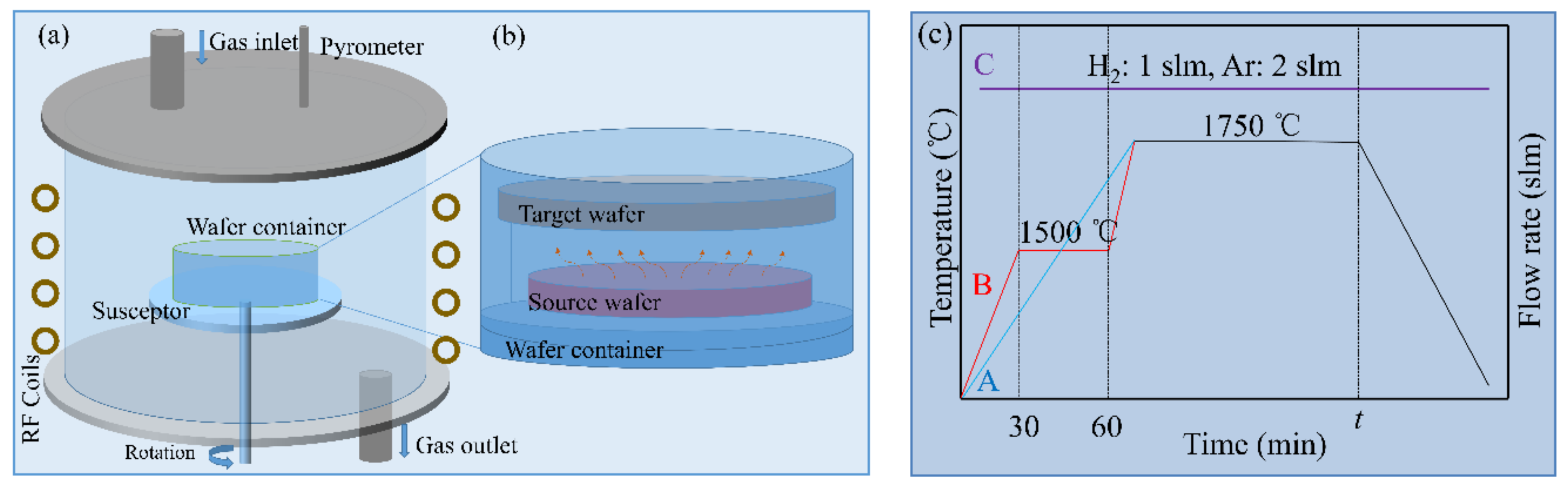
2.2. Apparatus
2.3. Methods
3. Results and Discussion
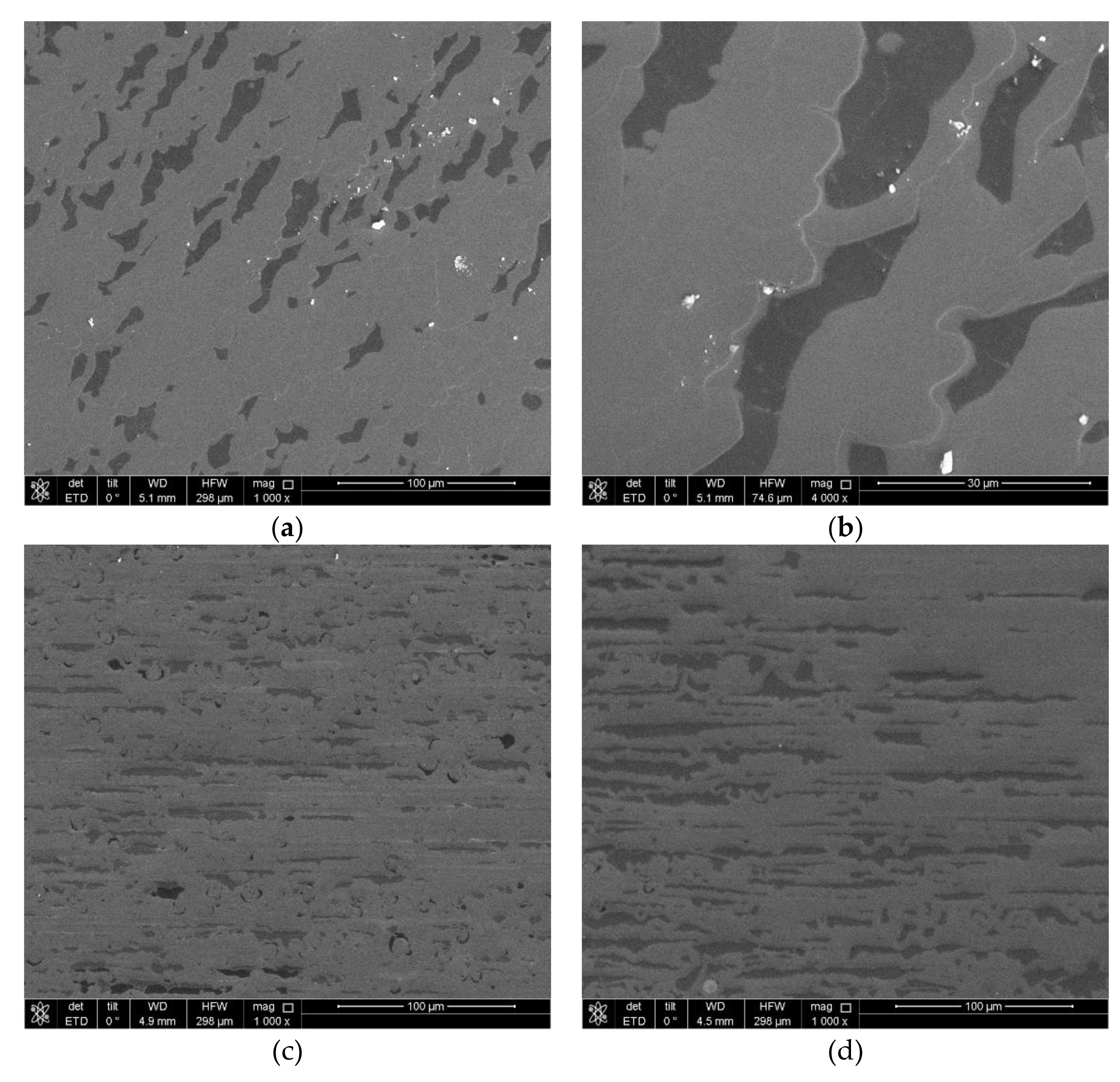
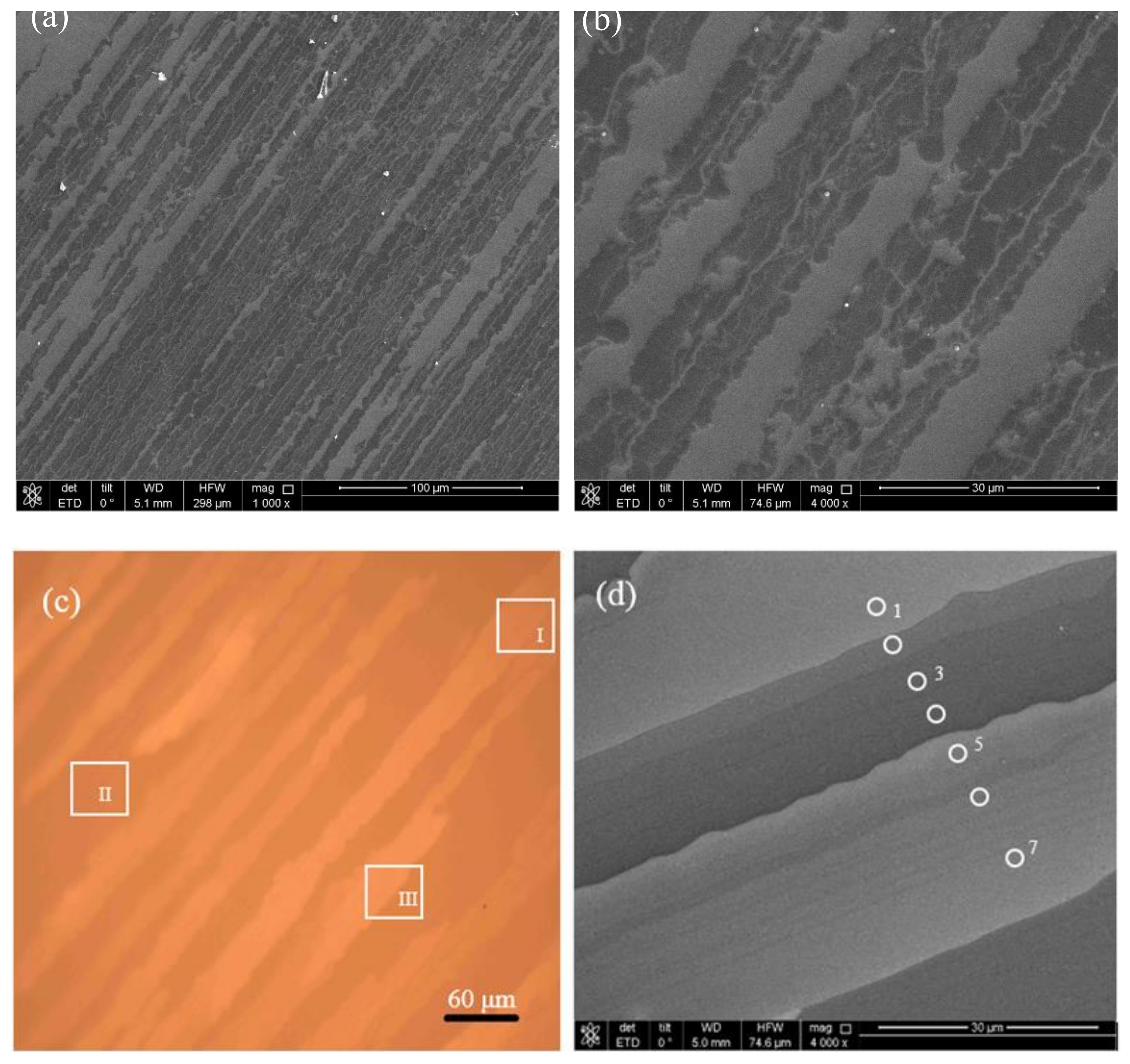
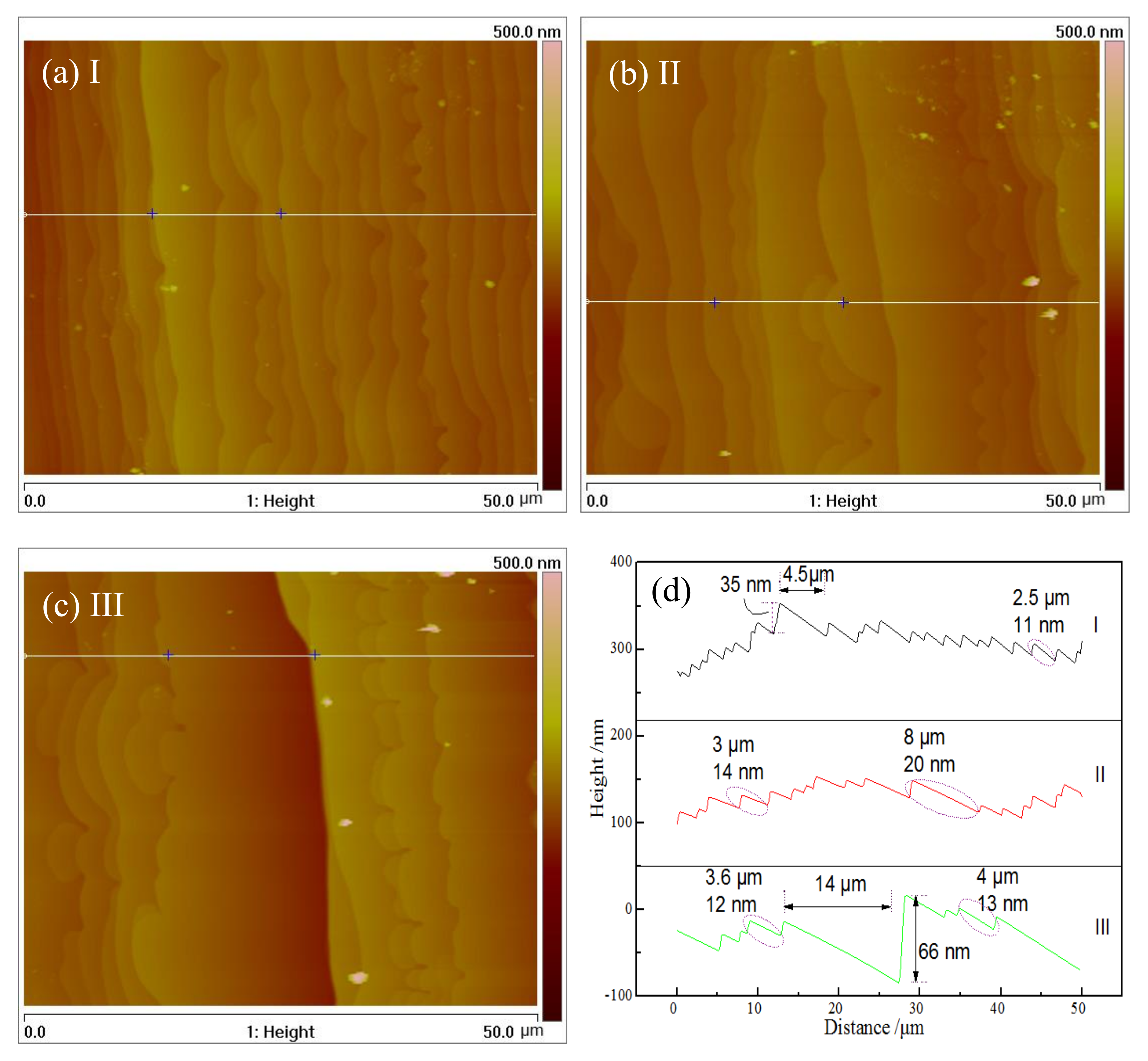
3.1. Effect of Heat Treatment
3.2. Role of Gas Mixture
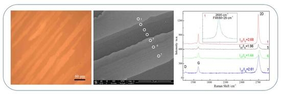
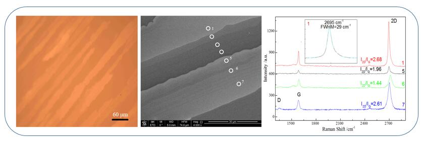
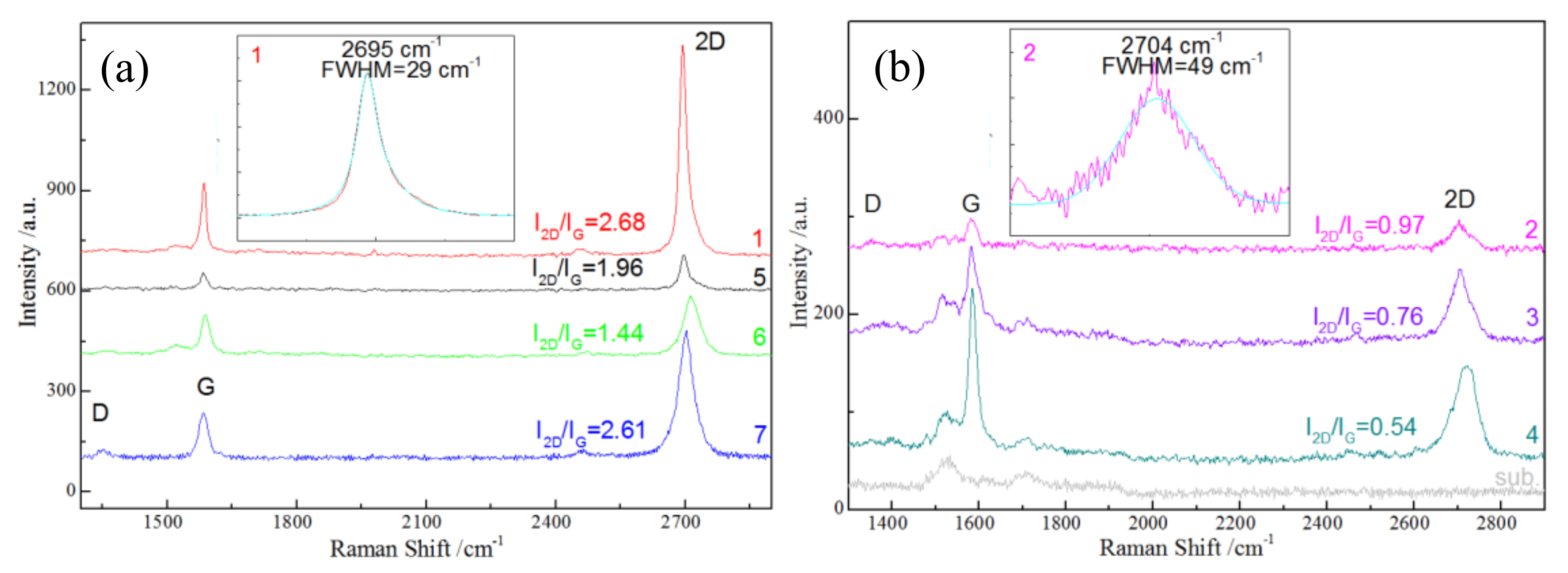
3.3. Graphene Characterization
4. Conclusions
Supplementary Materials
Author Contributions
Acknowledgments
Conflicts of Interest
References
- Zhang, Y.B.; Tan, Y.W.; Stormer, H.L.; Kim, P. Experimental observation of the quantum Hall effect and Berry’s phase in graphene. Nature 2005, 438, 201–204. [Google Scholar] [CrossRef] [PubMed]
- Ding, K.-H.; Lim, L.-K.; Su, G.; Weng, Z.-Y. Quantum Hall effect in ac driven graphene: From the half-integer to the integer case. Phys. Rev. B 2018, 97, 035123. [Google Scholar] [CrossRef] [Green Version]
- Novoselov, K.S.; Geim, A.K.; Morozov, S.V.; Jiang, D.; Katsnelson, M.I.; Grigorieva, I.V.; Dubonos, S.V.; Firsov, A.A. Two-dimensional gas of massless Dirac fermions in graphene. Nature 2005, 438, 197–200. [Google Scholar] [CrossRef] [PubMed] [Green Version]
- Luo, C.W.; Tseng, P.S.; Chen, H.J.; Wu, K.H.; Li, L.J. Dirac fermion relaxation and energy loss rate near the Fermi surface in monolayer and multilayer graphene. Nanoscale 2014, 6, 8575–8578. [Google Scholar] [CrossRef] [PubMed]
- Geim, A.K.; Novoselov, K.S. The rise of graphene. Nat. Mat. 2007, 6, 183–191. [Google Scholar] [CrossRef] [PubMed]
- Ren, S.; Rong, P.; Yu, Q. Preparations, properties and applications of graphene in functional devices: A concise review. Ceram. Int. 2018, 44, 11940–11955. [Google Scholar] [CrossRef]
- Zhou, K.G.; Vasu, K.S.; Cherian, C.T.; Neek-Amal, M.; Zhang, J.C.; Ghorbanfekr-Kalashami, H.; Huang, K.; Marshall, O.P.; Kravets, V.G.; Abraham, J.; et al. Electrically controlled water permeation through graphene oxide membranes. Nature 2018, 559, 236–240. [Google Scholar] [CrossRef] [PubMed]
- Politano, A.; Cattelan, M.; Boukhvalov, D.W.; Campi, D.; Cupolillo, A.; Agnoli, S.; Apostol, N.G.; Lacovig, P.; Lizzit, S.; Farias, D.; et al. Unveiling the Mechanisms Leading to H-2 Production Promoted by Water Decomposition on Epitaxial Graphene at Room Temperature. ACS Nano 2016, 10, 4543–4549. [Google Scholar] [CrossRef] [PubMed]
- Koppens, F.H.L.; Mueller, T.; Avouris, P.; Ferrari, A.C.; Vitiello, M.S.; Polini, M. Photodetectors based on graphene, other two-dimensional materials and hybrid systems. Nat. Nanotechnol. 2014, 9, 780–793. [Google Scholar] [CrossRef] [PubMed]
- Politano, A.; Chiarello, G. Plasmon modes in graphene: Status and prospect. Nanoscale 2014, 6, 10927–10940. [Google Scholar] [CrossRef] [PubMed]
- Novoselov, K.S.; Geim, A.K.; Morozov, S.V.; Jiang, D.; Zhang, Y.; Dubonos, S.V.; Grigorieva, I.V.; Firsov, A.A. Electric field effect in atomically thin carbon films. Science 2004, 306, 666–669. [Google Scholar] [CrossRef] [PubMed]
- Bointon, T.H.; Barnes, M.D.; Russo, S.; Craciun, M.F. High Quality Monolayer Graphene Synthesized by Resistive Heating Cold Wall Chemical Vapor Deposition. Adv. Mater. 2015, 27, 4200–4206. [Google Scholar] [CrossRef] [PubMed] [Green Version]
- Lee, H.C.; Jo, S.B.; Lee, E.; Yoo, M.S.; Kim, H.H.; Lee, S.K.; Lee, W.H.; Cho, K. Facet-Mediated Growth of High-Quality Monolayer Graphene on Arbitrarily Rough Copper Surfaces. Adv. Mater. 2016, 28, 2010–2014. [Google Scholar] [CrossRef] [PubMed]
- Chen, X.; Xiang, R.; Zhao, P.; An, H.; Inoue, T.; Chiashi, S.; Maruyama, S. Chemical vapor deposition growth of large single-crystal bernal-stacked bilayer graphene from ethanol. Carbon 2016, 107, 852–856. [Google Scholar] [CrossRef]
- Wu, J.; Wang, J.; Pan, D.; Li, Y.; Jiang, C.; Li, Y.; Jin, C.; Wang, K.; Song, F.; Wang, G.; et al. Synchronous Growth of High-Quality Bilayer Bernal Graphene: From Hexagonal Single-Crystal Domains to Wafer-Scale Homogeneous Films. Adv. Funct. Mater. 2017, 27, 1605927. [Google Scholar] [CrossRef]
- Gibson, K.D.; Sibener, S.J. Growth, Structure, and Vibrational Properties of Few Layer Graphene Grown on Rh(111). J. Phys. Chem. C 2016, 120, 24158–24164. [Google Scholar] [CrossRef]
- Soares, G.V.; Nakhaie, S.; Heilmann, M.; Riechert, H.; Lopes, J.M.J. Growth of boron-doped few-layer graphene by molecular beam epitaxy. Appl. Phys. Lett. 2018, 112, 163103. [Google Scholar] [CrossRef] [Green Version]
- Weibel, A.; Mesguich, D.; Chevallier, G.; Flahaut, E.; Laurent, C. Fast and easy preparation of few-layered-graphene/magnesia powders for strong, hard and electrically conducting composites. Carbon 2018, 136, 270–279. [Google Scholar] [CrossRef]
- Kairi, M.I.; Dayou, S.; Kairi, N.I.; Abu Bakar, S.; Vigolo, B.; Mohamed, A.R. Toward high production of graphene flakes—A review on recent developments in their synthesis methods and scalability. J. Mater. Chem. A 2018, 6, 15010–15026. [Google Scholar] [CrossRef]
- Badri, M.A.S.; Salleh, M.M.; Noor, N.F.a.M.; Abd Rahman, M.Y.; Umar, A.A. Green synthesis of few-layered graphene from aqueous processed graphite exfoliation for graphene thin film preparation. Mater. Chem. Phys. 2017, 193, 212–219. [Google Scholar] [CrossRef]
- Han, M.Y.; Oezyilmaz, B.; Zhang, Y.; Kim, P. Energy band-gap engineering of graphene nanoribbons. Phys. Rev. Lett. 2007, 98, 206805. [Google Scholar] [CrossRef] [PubMed]
- Li, X.; Wang, X.; Zhang, L.; Lee, S.; Dai, H. Chemically derived, ultrasmooth graphene nanoribbon semiconductors. Science 2008, 319, 1229–1232. [Google Scholar] [CrossRef] [PubMed]
- Luo, W.-G.; Wang, H.-F.; Cai, K.-M.; Han, W.-P.; Tan, P.-H.; Hu, P.-A.; Wang, K.-Y. Synthesis of Homogenous Bilayer Graphene on Industrial Cu Foil. Chin. Phys. Lett. 2014, 31, 067202. [Google Scholar] [CrossRef]
- Pang, J.; Bachmatiuk, A.; Fu, L.; Yan, C.; Zeng, M.; Wang, J.; Trzebicka, B.; Gemming, T.; Eckert, J.; Rummeli, M.H. Oxidation as A Means to Remove Surface Contaminants on Cu Foil Prior to Graphene Growth by Chemical Vapor Deposition. J. Phys. Chem. C 2015, 119, 13363–13368. [Google Scholar] [CrossRef]
- Xu, X.; Zhang, Z.; Dong, J.; Yi, D.; Niu, J.; Wu, M.; Lin, L.; Yin, R.; Li, M.; Zhou, J.; et al. Ultrafast epitaxial growth of metre-sized single-crystal graphene on industrial Cu foil. Sci. Bull. 2017, 62, 1074–1080. [Google Scholar] [CrossRef] [Green Version]
- Wang, C.; Chen, W.; Han, C.; Wang, G.; Tang, B.; Tang, C.; Wang, Y.; Zou, W.; Chen, W.; Zhang, X.-A.; et al. Growth of Millimeter-Size Single Crystal Graphene on Cu Foils by Circumfluence Chemical Vapor Deposition. Sci. Rep. 2014, 4, 4537. [Google Scholar] [CrossRef] [PubMed]
- Li, X.; Cai, W.; An, J.; Kim, S.; Nah, J.; Yang, D.; Piner, R.; Velamakanni, A.; Jung, I.; Tutuc, E.; et al. Large-Area Synthesis of High-Quality and Uniform Graphene Films on Copper Foils. Science 2009, 324, 1312–1314. [Google Scholar] [CrossRef] [PubMed] [Green Version]
- Xin, H.; Li, W. A review on high throughput roll-to-roll manufacturing of chemical vapor deposition graphene. Appl. Phys. Rev. 2018, 5, 031105. [Google Scholar] [CrossRef]
- Li, J.; Wang, X.-Y.; Liu, X.-R.; Jin, Z.; Wang, D.; Wan, L.-J. Facile growth of centimeter-sized single-crystal graphene on copper foil at atmospheric pressure. J. Mater. Chem. C 2015, 3, 3530–3535. [Google Scholar] [CrossRef]
- Cai, S.; Liu, Z.; Zhong, N.; Liu, S.; Liu, X. Effect of Growth Pressure on Epitaxial Graphene Grown on 4H-SiC Substrates by Using Ethene Chemical Vapor Deposition. Materials 2015, 8, 5586–5596. [Google Scholar] [CrossRef] [PubMed] [Green Version]
- Cai, T.; Jia, Z.; Yan, B.; Yu, D.; Wu, X. Hydrogen assisted growth of high quality epitaxial graphene on the C-face of 4H-SiC. Appl. Phys. Lett. 2015, 106, 013106. [Google Scholar] [CrossRef] [Green Version]
- Hassan, J.; Winters, M.; Ivanov, I.G.; Habibpour, O.; Zirath, H.; Rorsman, N.; Janzen, E. Quasi-free-standing monolayer and bilayer graphene growth on homoepitaxial on-axis 4H-SiC(0001) layers. Carbon 2015, 82, 12–23. [Google Scholar] [CrossRef]
- Liu, Q.; Yu, C.; He, Z.; Gu, G.; Wang, J.; Zhou, C.; Guo, J.; Gao, X.; Feng, Z. Chemical vapor deposition graphene of high mobility by gradient growth method on an 4H-SiC (0001) substrate. Appl. Surf. Sci. 2018, 454, 68–73. [Google Scholar] [CrossRef]
- Liu, X.; Chen, Y.; Sun, C.; Guan, M.; Zhang, Y.; Zhang, F.; Sun, G.; Zeng, Y. Surface Evolution of Nano-Textured 4H-SiC Homoepitaxial Layers after High Temperature Treatments: Morphology Characterization and Graphene Growth. Nanomaterials 2015, 5, 1532–1543. [Google Scholar] [CrossRef] [PubMed]
- Berger, C.; Song, Z.; Li, X.; Wu, X.; Brown, N.; Naud, C.; Mayou, D.; Li, T.; Hass, J.; Marchenkov, A.N.; et al. Electronic confinement and coherence in patterned epitaxial graphene. Science 2006, 312, 1191–1196. [Google Scholar] [CrossRef] [PubMed]
- Cai, S.; Liu, X.; Huang, J.; Liu, Z. Feasibility of polyethylene film as both supporting material for transfer and target substrate for flexible strain sensor of CVD graphene grown on Cu foil. RSC Adv. 2017, 7, 48333–48340. [Google Scholar] [CrossRef] [Green Version]
- Kim, W.; Kim, H.; Kim, G.T. Ultra-Easy and Fast Method for Transferring Graphene Grown on Metal Foil. Nano 2017, 12, 1750140. [Google Scholar] [CrossRef] [Green Version]
- Camara, N.; Tiberj, A.; Jouault, B.; Caboni, A.; Jabakhanji, B.; Mestres, N.; Godignon, P.; Camassel, J. Current status of self-organized epitaxial graphene ribbons on the C face of 6H-SiC substrates. J. Phys. D-Appl. Phys. 2010, 43, 374011. [Google Scholar] [CrossRef]
- Huang, Q.; Kim, J.J.; Ali, G.; Cho, S.O. Width-Tunable Graphene Nanoribbons on a SiC Substrate with a Controlled Step Height. Adv. Mater. 2013, 25, 1144–1148. [Google Scholar] [CrossRef] [PubMed]
- Bishop, S.M.; Reynolds, C.L., Jr.; Liliental-Weber, Z.; Uprety, Y.; Ebert, C.W.; Stevie, F.A.; Park, J.S.; Davis, R.F. Sublimation growth of an in-situ-deposited layer in SiC chemical vapor deposition on 4H-SiC(1 1 (2)over-bar 0). J. Cryst. Growth 2008, 311, 72–78. [Google Scholar] [CrossRef]
- Liu, B.; Sun, G.-S.; Liu, X.-F.; Zhang, F.; Dong, L.; Zheng, L.; Yan, G.-G.; Liu, S.-B.; Zhao, W.-S.; Wang, L.; et al. Fast Homoepitaxial Growth of 4H-SiC Films on 4 degrees off-Axis Substrates in a SiH4-C2H4-H-2 System. Chin. Phys. Lett. 2013, 30, 28101. [Google Scholar] [CrossRef]
- Ishida, Y.; Yoshida, S. Investigation of the giant step bunching induced by the etching of 4H-SiC in Ar-H-2 mix gases. Jpn. J. Appl. Phys. 2016, 55, 095501. [Google Scholar] [CrossRef]
- Kimoto, T.; Itoh, A.; Matsunami, H.; Okano, T. Step bunching mechanism in chemical vapor deposition of 6H- and 4H-SiC{0001}. J. Appl. Phys. 1997, 81, 3494–3500. [Google Scholar] [CrossRef]
- Tabuchi, Y.; Ashida, K.; Sonoda, M.; Kaneko, T.; Ohtani, N.; Katsuno, M.; Sato, S.; Tsuge, H.; Fujimoto, T. Wide (0001) terrace formation due to step bunching on a vicinal 4H-SiC (0001) epitaxial layer surface. J. Appl. Phys. 2017, 122, 075702. [Google Scholar] [CrossRef]
- Prakash, G.; Capano, M.A.; Bolen, M.L.; Zemlyanou, D.; Reifenberger, R.G. AFM study of ridges in few-layer epitaxial graphene grown on the carbon-face of 4H-SiC(000(1)over-bar). Carbon 2010, 48, 2383–2393. [Google Scholar] [CrossRef]
- Ushio, S.; Yoshii, A.; Tamai, N.; Ohtani, N.; Kaneko, T. Wide-range temperature dependence of epitaxial graphene growth on 4H-SiC (0 0 0-1): A study of ridge structures formation dynamics associated with temperature. J. Cryst. Growth 2011, 318, 590–594. [Google Scholar] [CrossRef]
- Bouhafs, C.; Darakchieva, V.; Persson, I.L.; Tiberj, A.; Persson, P.O.A.; Paillet, M.; Zahab, A.A.; Landois, P.; Juillaguet, S.; Schoeche, S.; et al. Structural properties and dielectric function of graphene grown by high-temperature sublimation on 4H-SiC(000-1). J. Appl. Phys. 2015, 117, 085701. [Google Scholar] [CrossRef]
- Krzyzewski, F. 4H-SiC surface structure transitions during crystal growth following bunching in a fast sublimation process. J. Cryst. Growth 2014, 401, 511–513. [Google Scholar] [CrossRef]
- Ferrari, A.C.; Meyer, J.C.; Scardaci, V.; Casiraghi, C.; Lazzeri, M.; Mauri, F.; Piscanec, S.; Jiang, D.; Novoselov, K.S.; Roth, S.; et al. Raman spectrum of graphene and graphene layers. Phys. Rev. Lett. 2006, 97, 187401. [Google Scholar] [CrossRef] [PubMed]
- Martins Ferreira, E.H.; Moutinho, M.V.O.; Stavale, F.; Lucchese, M.M.; Capaz, R.B.; Achete, C.A.; Jorio, A. Evolution of the Raman spectra from single-, few-, and many-layer graphene with increasing disorder. Phys. Rev. B 2010, 82, 125429. [Google Scholar] [CrossRef]
- Thomsen, C.; Reich, S. Doable resonant Raman scattering in graphite. Phys. Rev. Lett. 2000, 85, 5214–5217. [Google Scholar] [CrossRef] [PubMed]
- Strudwick, A.J.; Creeth, G.L.; Johansson, N.A.B.; Marrows, C.H. Probing residual strain in epitaxial graphene layers on 4H-SiC (000(1)over-bar) with Raman spectroscopy. Appl. Phys. Lett. 2011, 98, 051910. [Google Scholar] [CrossRef]
- Rana, T.; Chandrashekhar, M.V.S.; Sudarshan, T.S. Vapor phase surface preparation (etching) of 4H-SiC substrates using tetrafluorosilane (SiF4) in a hydrogen ambient for SiC epitaxy. J. Cryst. Growth 2013, 380, 61–67. [Google Scholar] [CrossRef]
- Dong, L.; Sun, G.; Yu, J.; Zheng, L.; Liu, X.; Zhang, F.; Yan, G.; Li, X.; Wang, Z. Growth of 4H-SiC epilayers with low surface roughness and morphological defects density on 4 degrees off-axis substrates. Appl. Surf. Sci. 2013, 270, 301–306. [Google Scholar] [CrossRef]


© 2018 by the authors. Licensee MDPI, Basel, Switzerland. This article is an open access article distributed under the terms and conditions of the Creative Commons Attribution (CC BY) license (http://creativecommons.org/licenses/by/4.0/).
Share and Cite
Cai, S.; Liu, X.; Zheng, X.; Liu, Z. Growth of Ordered Graphene Ribbons by Sublimation Epitaxy. Crystals 2018, 8, 449. https://doi.org/10.3390/cryst8120449
Cai S, Liu X, Zheng X, Liu Z. Growth of Ordered Graphene Ribbons by Sublimation Epitaxy. Crystals. 2018; 8(12):449. https://doi.org/10.3390/cryst8120449
Chicago/Turabian StyleCai, Shuxian, Xingfang Liu, Xin Zheng, and Zhonghua Liu. 2018. "Growth of Ordered Graphene Ribbons by Sublimation Epitaxy" Crystals 8, no. 12: 449. https://doi.org/10.3390/cryst8120449