Article

Investigation into the Effects of Cross-Sectional Shape and Size on the Light-Extraction Efficiency of GaN-Based Blue Nanorod Light-Emitting Diode Structures

Department of Physics, Inha University, 100 Inha-ro, Michuhol-gu, Incheon 22212, Republic of Korea
*
Author to whom correspondence should be addressed.
Crystals 2024, 14(3), 241; https://doi.org/10.3390/cryst14030241
Submission received: 25 January 2024 / Revised: 22 February 2024 / Accepted: 27 February 2024 / Published: 29 February 2024
(This article belongs to the Special Issue Group-III Nitride Quantum Wells)

Abstract

:
We investigated the effect of cross-sectional shape and size on the light-extraction efficiency (LEE) of GaN-based blue nanorod light-emitting diode (LED) structures using numerical simulations based on finite-difference time-domain methods. For accurate determination, the LEE and far-field pattern (FFP) were evaluated by averaging them over emission spectra, polarization, and source positions inside the nanorod. The LEE decreased as rod size increased, owing to the nanorods’ increased ratio of cross-sectional area to sidewall area. We compared circular, square, triangular, and hexagonal cross-sectional shapes in this study. To date, nanorod LEDs with circular cross sections have been mainly demonstrated experimentally. However, circular shapes were found to show the lowest LEE, which is attributed to the coupling with whispering-gallery modes. For the total emission of the nanorod, the triangular cross section exhibited the highest LEE. When the angular dependence of the LEE was calculated using the FFP simulation results, the triangular and hexagonal shapes showed relatively high LEEs for direction emission. The simulation results presented in this study are expected to be useful in designing high-efficiency nanorod LED structures with optimum nanorod shape and dimensions.

1. Introduction

Since the first demonstration of GaN-based light-emitting diodes (LEDs) in the early 1990s, GaN-based LEDs have been widely used in solid-state lighting and display applications, owing to their high efficiency and eco-friendliness [1,2,3,4,5,6]. Up to now, LED devices with an area of 300 × 300 μm2 have been intensively developed for use in illumination light sources for general lighting and liquid crystal displays. However, in recent years, micro- and nano-sized GaN LEDs have gained increasing interest, driven by nano-scale fabrication techniques and large-scale integration technologies. These miniaturized LEDs are expected to provide high efficiency and superior functionality in emerging microdisplay, biology, sensing, and visible light communication applications [7,8,9,10,11,12,13,14]. Micro-LEDs are considered to be ideal candidates for next-generation displays such as virtual reality (VR) and augmented reality (AR) smart glasses [15,16,17,18]. High-resolution and high-luminance AR and VR display applications require LED chip sizes on the order of micrometers or submicrometers. Accordingly, significant efforts have been put into developing micro/nano-LED arrays consisting of tiny pixels in the submicrometer size regime [19,20,21,22,23]. The development of GaN-based nanorod LEDs is expected to provide a significant advancement in display technology, offering unparalleled brightness, resolution, and miniaturization. The nanorod LED structure is expected to exhibit a high crystallinity with reduced stacking faults, threading dislocation densities, and piezoelectric polarization [24,25,26,27].
In addition, the large surface-to-volume ratio in nanorod structures enables efficient light extraction out of the nanorod LED, which can significantly increase light-extraction efficiency (LEE). The LEE of micro/nano-LED structures is believed to increase with decreasing device size [28,29,30,31]. For large-area planar LED structures, increasing the LEE has been a major technological challenge, as the LEE is limited by the total internal reflection (TIR). Due to the large difference in the refractive index between GaN materials and air, only a small fraction of light can be extracted from LED chips. Various techniques have been proposed to enhance the LEE of GaN-based LEDs, including surface roughness, patterned substrates, and photonic crystal or plasmonic structures [32,33,34,35,36]. Nanorod LED structures, with dimensions of a few hundred nanometers in diameter and a few micrometers in length, are expected to exhibit high LEE because the TIR can be easily spoiled in wavelength-sized structures. Several previous studies have demonstrated the enhancement of LEE in GaN-based nanorod LED structures [37,38,39,40,41].
LEE is defined as the ratio of external quantum efficiency (EQE) to internal quantum efficiency (IQE). While the EQE can be obtained experimentally, evaluating IQE through experimental measurements is not straightforward. Therefore, it is challenging to determine LEE with experimental methods. Therefore, the LEE of LED structures has mostly been studied using numerical simulations. Finite-difference time-domain (FDTD) methods have been widely employed in the simulation of wavelength-size nanophotonic structures where light interference and diffraction effects play an essential role. Because the FDTD method numerically solves four Maxwell’s equations without any assumptions or approximations, it can provide accurate simulation results of the optical properties in photonic devices. Therefore, studies on the LEE and light-emitting pattern of micro/nano-LED structures have been frequently conducted using the FDTD method [28,31,40,41,42,43,44,45,46].
The LEE in nanorod LED structures can be strongly dependent on chip size and geometry. For micro-LED structures with lateral sizes greater than 2 μm, the effects of chip size and cross-sectional shape on LEE have been investigated in several works of the literature. LEE in micro-LED structures was reported to decrease with increasing lateral size because the escape cone is reduced and light absorption increases with increasing chip size [28,47]. As the size of an LED chip approaches the wavelength of the emitted light, the LEE and emission patterns can vary greatly depending on the size and geometry of the LED structures [31]. For nanorod LED structures, however, the dependence of LEE on chip size and cross-sectional shape is relatively uninvestigated. Angular distribution of light emission from LEDs can be obtained using far-field pattern (FFP) simulation results. Thus, FFP characteristics can be important in micro-display and AR/VR display applications. However, few studies have been conducted to investigate the structural dependence of FFP in nanorod LEDs.
In this study, we investigate the effect of cross-sectional shape and size on the LEE and FFP of nanorod LED structures using three-dimensional (3D) FDTD simulation methods. In the FDTD method, a point dipole source is placed at a quantum-well (QW) position in the nanorod structure and the evolution of the electromagnetic fields is monitored, from which the LEE and emission distributions can be calculated. Because of the small chip dimensions on the wavelength scale, the LEE in the nanorod LED structure depends on the dipole source location and polarization direction [46]. However, most previous studies on FDTD simulations of nanorod LED structures reported simulation results for only a single dipole source, which was typically placed at the center of the nanorod structure [40,41,42,43,44,45]. This assumption may not provide realistic results for the LEE and FFP of nanorod LEDs. In the simulations of this study, the LEE and FFP of nanorod LEDs are averaged for dipole source positions, polarization directions, and spectral power distribution for accurate determination of LEE and FFP.
Until now, nanorod LEDs with mainly circular or hexagonal cross sections have been fabricated. A hexagonal cross section is the shape of a thermodynamically stable nanorod structure during epitaxial growth processes [48]. A circular cross section is usually formed with dry-etching processes. In addition to the circular and hexagonal shapes, triangular and square cross sections are also considered in this work. For each cross-sectional shape, we simulate LEE and FFP according to the size of the nanorod structure using 3D FDTD methods. Based on the simulation results, we discuss the optimum nanorod LED structures for achieving high LEE and desired emission characteristics.

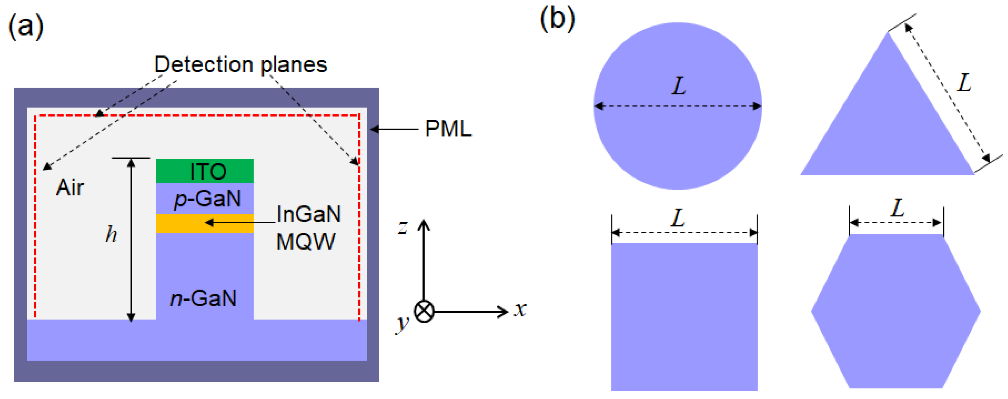
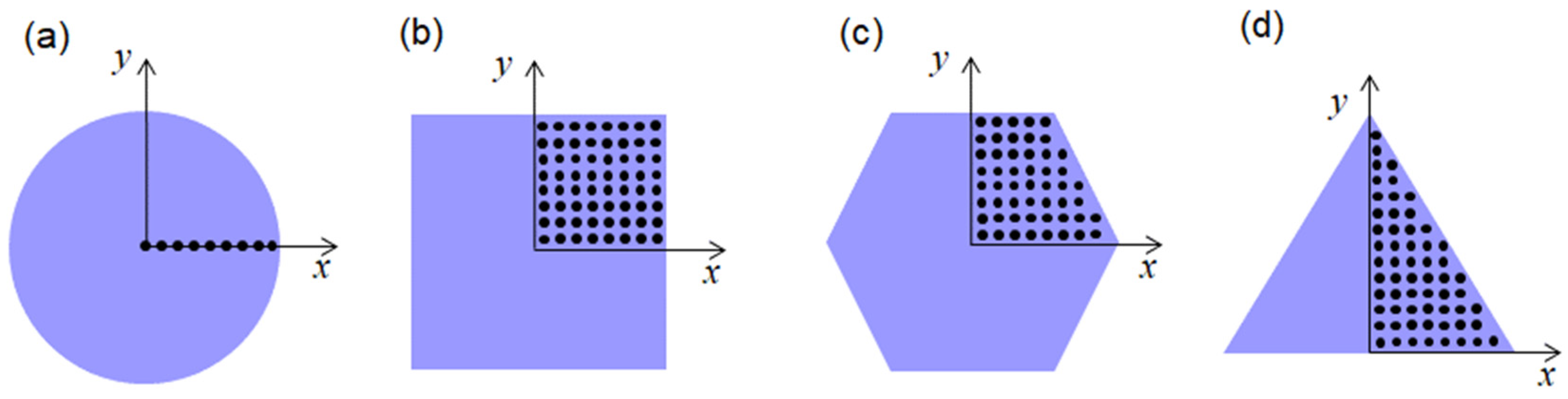
2. Simulation Methods

For the simulation of this study, a commercial FDTD program by Ansys/Lumerical Inc. was employed. Figure 1a schematically illustrates the side view of the simulated nanorod LED structure in the FDTD computational domain. Perfectly-matched-layer (PML) boundary conditions were imposed on all computational domain boundaries. The PML boundary condition refers to the free-space boundary condition in which all propagation light incident on the PML is completely absorbed without reflection. In the simulation structure of this work, a nanorod LED structure with a height of h was formed on the n-GaN substrate. The LED epitaxial layers consisted of an n-GaN layer, a 50 nm InGaN/GaN multiple-quantum-well (MQW) active region, and a 20 nm p-GaN layer. A 100 nm indium-tin-oxide (ITO) layer was positioned on p-GaN for the current injection. The simulated nanorod LED structure was assumed to be exposed to air. Metal electrodes were not included in the simulation domain. The reflection from below the substrate may affect the LEE and FFP of the simulation results. However, we did not include this effect of substrate reflection, under the assumption that light propagating in the substrate direction is not reflected toward the nanorod LED structure.
The refractive index of GaN was set to 2.45, and the InGaN/GaN MQW active region was modeled as a uniform medium with an effective refractive index of 2.49 [49]. The complex refractive index of ITO was set to 1.94 + 0.015 i [50]. The absorption coefficients of the GaN and InGaN MQW regions were assumed to be 20 and 1000 cm−1, respectively [51]. In fact, there exists some difference between the reported absorption coefficient values, and it is not easy to know the actual absorption coefficient values. However, this ambiguity of the absorption coefficients has little influence on the relative comparison of LEE between different cross-sectional shapes and sizes.
For the nanorod LED structure of this study, we investigated four types of cross sections: circular, square, equilateral triangular, and regular hexagonal shape. Figure 1b shows cross-sectional shapes in the x-y plane for the simulated nanorod LED structures. The diameter of the circle and the side lengths of the equilateral triangle, square, and regular hexagon are denoted as L. We performed FDTD simulations and calculated LEE with varying L for each cross-sectional shape. Here, the rod height h was fixed at 3 μm. We found from a separate simulation that the LEE does not depend significantly on h. In the simulation, the range of L varied from 200 to 1000 nm for the circle, 200 to 800 nm for the square, 300 to 1200 nm for the triangle, and 100 to 500 nm for the hexagon, respectively.
In the FDTD simulations, the electron-hole radiative recombination in semiconductors can be simplified to dipole radiation placed in the middle of the MQW region. In most LEDs operating in the visible wavelength range, light is emitted mostly in the transverse electric mode, corresponding to the polarization direction in the plane of the QWs [52,53,54,55]. Thus, assuming that the contribution of light polarized in the z direction was negligible, we considered only the x and y directions of the dipole source polarization. To simulate light emission from the QW, a dipole source was excited at the midpoint of the active region in the z direction. The dipole source spectrum was assumed to be a Gaussian lineshape function with a peak wavelength of 450 nm and a full width at a half-maximum of 15 nm, similar to the spectral power distribution (SPD) of typical InGaN blue LEDs.
To evaluate the LEE, the total dipole radiation power was first calculated in a small box surrounding the dipole source. Next, the radiation power outside the LED chip was calculated on the detection planes near the PML boundaries, as indicated by dotted lines in Figure 1a. The LEE was then determined as the ratio of the power on the detection planes to the total radiated power. The FFP of a nanorod LED was obtained with the Fourier transform of electromagnetic fields on the detection planes, which corresponds to the Fraunhofer diffraction pattern of light emitted from the nanorod surfaces. The FFPs from five detection planes surrounding the nanorod were merged, and an angular distribution of emissions and LEE was obtained.
For the accurate determination of the LEE and FFP of nanorod LED structures, simulation results were averaged over dipole source positions, polarizations, and SPDs. For each FDTD simulation, a single dipole source with specific position and polarization was employed. Then, the FDTD simulation results for different source positions and polarizations were summed to obtain the averaged results for LEE and FFP. The LEE at position (x, y) in the QW plane with polarization state p, which is denoted as η p ( x , y ) , is obtained by considering the spectral average of the source spectrum. That is,
η p ( x , y ) = η p λ ( x , y ) S ( λ ) d λ S ( λ ) d λ
where η p λ ( x , y ) is the LEE at position (x, y) and wavelength λ with the polarization state p, and S(λ) is the SPD of the dipole source. For each source position, there are two orthogonal polarization directions: x-polarization and y-polarization. Thus, the overall LEE (η) averaged for the active area and two polarization directions can be obtained as follows:
η = p = 1 , 2 a r e a η p ( x , y ) d x d y 2 a r e a d x d y
Dipole source points should be uniformly distributed in the x-y plane of the active area. To reduce the simulation time, the symmetry of the cross-sectional shape was used to reduce the number of source points. Figure 2 shows the actual simulated source points for each cross section. The solid dots inside each LED structure indicate the locations of the dipole sources used for the FDTD simulations. For circular cross sections, LEE and FFP can be obtained accurately by simulating for positive source points only in the x direction, using its circular symmetry. In this case, the average LEE for circular nanorods with a radius R is simplified as follows [46]:
η = p = 1 , 2 0 R η p ( x ) ( 2 π x ) d x 2 ( π R 2 ) = 1 R 2 p = 1 , 2 0 R η p ( x ) x d x
For square and hexagonal cross sections, it is sufficient to choose the source points in the first quadrant to obtain the average LEE and FFP. For triangular cross sections, it is necessary to simulate half the source points in the x-y plane.
As the number of source points increases, the accuracy of simulation results will be improved at the cost of a longer simulation time. We first investigated the dependence of LEE on the dipole source spacing. LEE was simulated as the source spacing for the circular and square cross sections. Figure 3 shows the average LEE calculated using Equation (2) for circular and square cross sections with D of 500 nm. The LEE increased only slightly with increasing source spacing. As the source spacing increased from 10 to 40 nm, the average LEE increased relatively by ~0.7% and ~1.5% for the circular and square cross sections, respectively. When the source spacing was 25 nm, the relative increases in LEE for the circular and square cross sections were less than 0.2% and 0.3%, respectively. Thus, when the source spacing is 25 nm, the numerical error due to the source spacing is almost negligible, so we chose the spacing to be 25 nm for simulations of this study.

3. Results and Discussion

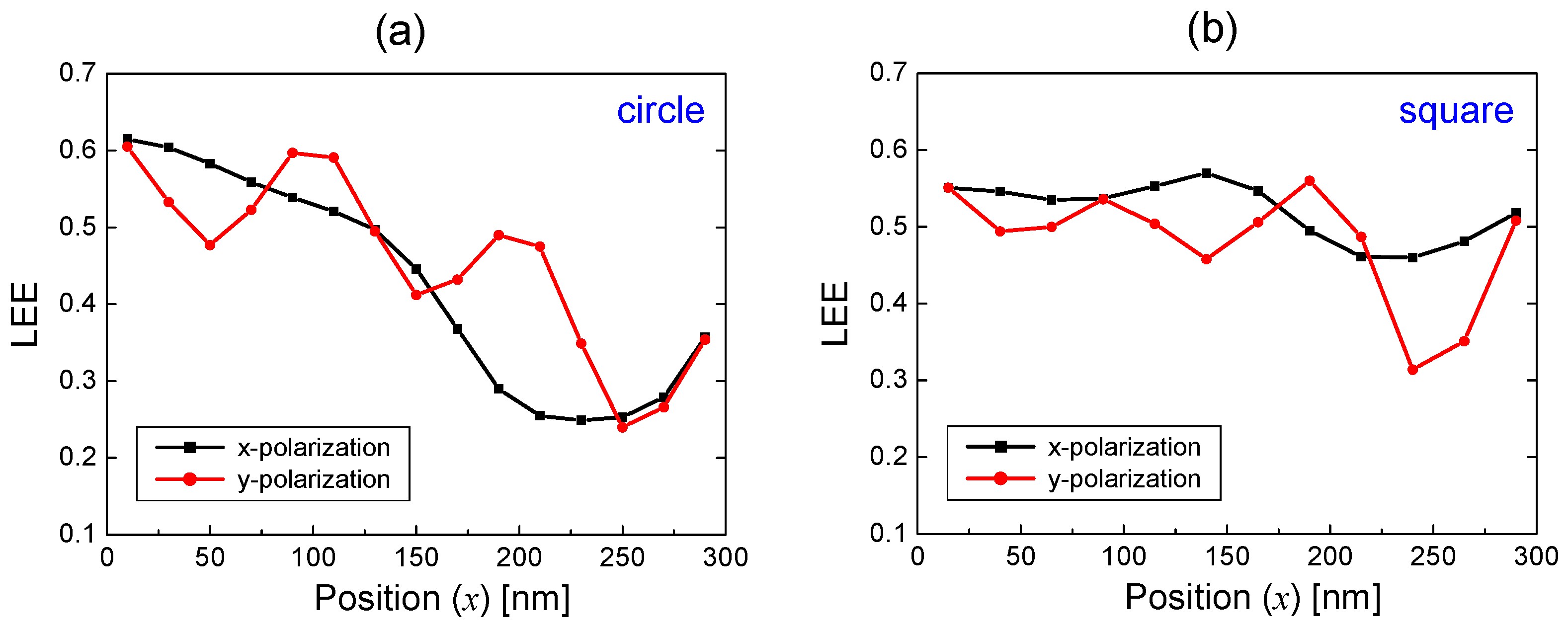
3.1. Effects of Source Position and Polarization on LEE

We investigated the dependence of LEE on the source position and polarization for circular and square cross sections. Figure 4 shows the spectrally averaged LEE in Equation (1) for circular and square nanorods with L = 0.6 μm. LEE is plotted as a function of the source position in the x direction when y = 0. The LEE for circular nanorods mostly exhibited decreasing behaviors with increasing source position, especially for the x-polarization mode. The LEE was ~60% near the center and decreased to below 30% as the source point approached the rod edge. This significant decrease in LEE near the edge of the circular rod is attributed to the coupling of the dipole source with the whispering-gallery mode (WGM) [28,46]. WGMs exist along the circumference of the circular nanorod and generally have a very long photon lifetime inside the rod. Light coupled with the WGM thus exits the rod quite slowly, resulting in a low LEE. Because WGMs are polarized in the radial direction, x-polarized dipole sources with large x values can strongly couple with the WGMs, thus showing low LEE values. For the y-polarized dipole sources, the coupling with WGMs is relatively weak. Thus, the decrease in the LEE of the y-polarized dipole source with large x values can be attributed to the coupling with radial modes that oscillate in the direction of the rod diameter. The y-polarized dipole sources can strongly couple with radial modes oscillating in the x-axis, which has a polarization in the y direction. Therefore, the fluctuations in LEE observed in the y-polarization mode are attributed to coupling with radially oscillating modes that have polarizations in the y direction [46].
For square nanorods, there is no significant decrease in LEE as the source position increases compared with that for circular nanorods. This is due to the absence of WGMs in square cross sections. Thus, square nanorods are expected to exhibit higher LEEs than circular ones when the LEE values are averaged over source positions. At several source positions in the y-polarization mode, the LEE decreased relatively significantly, which appears to be caused by the coupling of radial modes, as observed in the circular cross section. Triangular and hexagonal cross sections do not support WGMs, as is the case for the square cross section. Therefore, the average LEE of the triangular and hexagonal nanorod LEDs is also expected to be higher than that of the circular nanorods.

3.2. Dependence of LEE on Nanorod Shape and Size

Using the source position- and polarization-dependent LEE data in Figure 4 and Equation (2), the LEE averaged over source positions and polarization directions can be obtained. In Figure 5, the average LEE is plotted as a function of L for the circular, square, triangular, and hexagonal cross sections. The average LEE tends to decrease in all cross-sectional features with increasing L. In simulated nanorod LED structures, light is mainly extracted into the air through the sidewall surface because the rod height h is much longer than L. As L increases, the sidewall surface area increases linearly with L, while the floor area adjacent to the substrate increases quadratically with L. Therefore, as L increases, the LEE to the air will decrease, while the portion of light exiting to the substrate direction will increase. It can be seen that the circular cross section shows a more rapid decrease in average LEE than other cross sections, which can be attributed to the strong coupling of WGMs in the circular cross section, as shown in Figure 4. However, it may be inappropriate to compare LEEs between different cross-sectional shapes for the same L value. Instead, comparing LEEs for the same cross-sectional areas would be fair.
Figure 6 shows the average LEE as a function of cross-sectional area (A) for the four cross-sectional shapes. When A is less than 0.1 μm2, the circular nanorod exhibited the highest LEE, which could be as high as 70%. On the contrary, the circular nanorod showed the lowest LEE for A greater than 0.2 μm2. As mentioned earlier, the presence of a WGM prevents photons from escaping into the air from the circular cross section. Because the quality factor of WGM increases with disk size, the LEE of a circular rod can be decreased significantly by increasing A. When A is larger than 0.1 μm2, the triangular nanorod exhibited the highest LEE among the four cross-sectional shapes, implying that the triangular cross-sectional shape is the most efficient in extracting light from the nanorod structure for sufficiently large nanorod size. When A is larger than 0.2 μm2, the LEE difference between the triangular and circular nanorods is greater than 10%. The average LEE of the square and hexagonal cross sections showed similar values for all cross-sectional areas. The decrease in average LEE with increasing A, observed in all cross-sectional shapes, resulted from the relative increase in light extraction through the substrate direction with the increase in A, as described in Figure 4. In addition, the increase in the light absorption inside the nanorod with increasing nanorod volume also led to a decrease in the overall LEE with increasing A.

3.3. Electric Field Intensity Profiles

Figure 7 shows the electric field intensity profiles in the plane of QWs for circular, triangular, and hexagonal cross-sectional shapes with various L values. The intensity profiles were averaged over SPD, polarizations, and source positions as in the calculation of the average LEE. For circular cross sections, both WGM and Fabry–Perot radial modes are observed. A strong electric field intensity around the circular boundary corresponds to the WGMs. As L increases, the electric field intensity near the central region inside the rod was reduced relative to that of the circular rim, implying that the influence of WGMs becomes stronger with increasing diameter. In Figure 7b,c, electric field profiles with triangular and hexagonal symmetries are observed for triangular and hexagonal cross sections, respectively. In both triangular and hexagonal cross sections, relatively high intensities are observed near the boundaries of the nanorods, similar to the WGM of circular nanorods. However, the electric field intensity decreased significantly near the vertices of the triangular and hexagonal cross sections, which is distinct from the WGM of the circular nanorods.
Figure 8 shows the near-field emission profiles above the nanorod LED structure for the four cross-sectional shapes when L is 400 nm. The emission profile corresponds to the electric-field intensity distribution calculated from the detection plane above the nanorod in Figure 1. The emission profiles in Figure 8 were also averaged over SPD, polarizations, and source positions, as in Figure 7. For each cross-sectional shape, signatures of the circular, triangular, square, and hexagonal symmetries can be observed. The sharp vertices of the polygon are smoothed due to the spectral and areal averaging effects, implying that reasonably uniform emission can be obtained for the triangular, square, and hexagonal nanorods as well as the circular ones.

3.4. Angular Dependence of LEE

Some applications of LEDs may require directional emission, and only light within a small solid angle can be used. Therefore, it is necessary to calculate the angular distribution of emission patterns to obtain the LEE value within a specified solid angle. For this purpose, FFP was calculated as a function of the polar angle (θ) and the azimuthal angle (ϕ). The FFP of a nanorod structure was obtained with the Fourier transform of the electromagnetic fields on the detection planes surrounding the nanorod, as shown in Figure 1a. The FFP was also averaged for spectral distribution, polarizations, and source positions.
Figure 9 shows the polar plots of simulated FFPs for various cross-sectional shapes and sizes. This plot averaged the FFP in the azimuthal direction and shows the angular distribution for the polar angle from 0 to 90 degrees. The emission in the vertical and horizontal directions corresponds to θ of 0 and 90°, respectively. In Figure 9, it can be seen that the FFP varies significantly depending on the cross-sectional shape and rod size. FFPs appear as a result of the complex interference and diffraction effects in nanorod structures. Thus, FFPs may strongly depend on the rod size and geometry. The half-wavelength inside the GaN blue nanorod is ~90 nm. Therefore, FFPs can vary significantly for only a 100 nm change in rod dimensions, as observed in Figure 9. For circular cross sections, a Lambertian-like profile is observed when L is 200 nm, and strong emission in the horizontal direction is observed when L is from 300 to 500 nm. For square cross sections, strong horizontal emission is observed for L of 200 nm, whereas the vertical emission is relatively strong for L of 300 and 400 nm. For triangular cross sections, broad emission for a wide range of polar angles is observed for L of 300 and 800 nm, and the vertical emission is relatively strong for L of 400 and 600 nm. For hexagonal cross sections, relatively strong vertical emission is observed for L of 100 to 300 nm. Thus, hexagonal nanorod LEDs with side lengths smaller than 300 nm can be advantageous for obtaining directional emission in the vertical direction.
The angular distribution of the FFP can be used to obtain the LEE within a specified collection polar angle θc. It can be obtained using the following formula:
η ( θ c ) = η total × 0 2 π d ϕ 0 θ c P ( θ , ϕ ) sin θ d θ 0 2 π d ϕ 0 π P ( θ , ϕ ) sin θ d θ
where P(θ, ϕ) is the radiation power at the polar angle θ and the azimuthal angle ϕ; P(θ, ϕ) is the radiation power averaged for spectrum, source positions, and polarizations; and ηtotal is the total LEE, which corresponds to the results in Figure 5. Thus, when θc is 180°, η(θc) is equal to the total LEE. The η(90°) corresponds to the LEE for the light emitted in the upper hemisphere. Figure 10 shows η(θc) calculated from Equation (4) as a function of θc for circular, square, triangular, and hexagonal cross sections. The LEE increases rapidly with increasing collection angles for all cross-sectional features. For small values of θc, the LEE will increase superlinearly with θc because the solid angle occupied by θc is quadratically proportional to θc. For example, for the circular cross section with L of 200 nm, η(90°) is ~45%. However, η(15°) and η(30°) are decreased to ~2% and ~8%, respectively.
In addition, the LEE shows a decreasing behavior with increasing L, as observed in Figure 5. For the square cross section, however, the LEE for L of 200 nm is lower than the LEE for L of 300 nm when θc is less than 40°. This is because the intensity in the vertical direction is relatively weak for angles of 40° or less, as shown in Figure 9b. For the hexagonal cross section, the average LEE for L of 100 nm is significantly higher than the average LEE for other L values, which is attributed to the strong vertical emission for L of 100 nm, as observed in Figure 9d.
In Figure 11, the LEE for θc of 15° and 30° is depicted as a function of the cross-sectional area (A) for the circular, triangular, square, and hexagonal nanorods. For the same cross-sectional shape and area, η(30°) was at least three times higher than η(15°). This is because the solid angle occupied by θc of 30° is ~4 times as large as that occupied by θc of 15°. However, the dependence of LEE on the cross-sectional shape and area is similar for the two collection angles. Triangular and hexagonal nanorods show relatively higher η(15°) and η(30°) values compared with circular and square nanorods when A is smaller than 0.3 μm2, which is attributed to the relatively strong emission in the vertical direction for triangular and hexagonal nanorods, as shown in Figure 9. Hexagonal nanorods exhibited the highest LEE for A less than 0.05 μm2. When A is larger than 0.3 μm2, the difference in LEE between different cross-sectional shapes was greatly reduced, implying that not all emission profiles are significantly affected by cross-sectional shapes for a relatively large nanorod size.

4. Conclusions

We numerically investigated the effects of cross-sectional shapes and areas on the LEE and FFP of nanorod LED structures using 3D FDTD simulations. The LEE was evaluated by averaging over the emission spectrum, polarization, and source positions for accurate determination. Circular, square, triangular, and hexagonal cross-sectional shapes were considered in this study. Until now, nanorod LEDs with circular cross sections have been mainly demonstrated experimentally. However, the simulation results indicated that the circular nanorod LED showed a lower LEE than other nanorod shapes. It was found that the triangular shape exhibited the highest LEE for the total emission from the nanorod, and the triangular and hexagonal shapes were found to be advantageous in obtaining a higher LEE for the directional emission with polar angles of < 30°. The LEE decreased as the rod size increased due to the increased ratio of cross-sectional area to sidewall area. The simulation results presented in this work are expected to provide the optimum nanorod shape and size for high-efficiency nanorod LEDs.

Author Contributions

Conceptualization, H.-Y.R.; methodology, B.L. and H.-Y.R.; software, B.L. and H.-Y.R.; validation, H.-Y.R.; investigation, B.L.; data curation, B.L.; writing—original draft preparation, B.L.; writing—review and editing, H.-Y.R.; supervision, H.-Y.R.; project administration, H.-Y.R.; funding acquisition, H.-Y.R. All authors have read and agreed to the published version of the manuscript.

Funding

This research was supported by an Inha University research grant.

Data Availability Statement

The original contributions presented in the study are included in the article, further inquiries can be directed to the corresponding author.

Conflicts of Interest

The authors declare no conflicts of interest.

References

  1. Pust, P.; Schmidt, P.J.; Schnick, W. A revolution in lighting. Nat. Mater. 2015, 14, 454–458. [Google Scholar] [CrossRef]
  2. Bhardwaj, J.; Cesaratto, J.M.; Wildeson, I.H.; Choy, H.; Tandon, A.; Soer, W.A.; Schmidt, P.J.; Spinger, B.; Deb, P.; Shchekin, O.B.; et al. Progress in high-luminance LED technology for solid-state lighting. Phys. Status Solidi A 2017, 214, 1600826. [Google Scholar] [CrossRef]
  3. Cho, J.; Park, J.H.; Kim, J.K.; Schubert, E.F. White light-emitting diodes: History, progress, and future. Laser Photonics Rev. 2017, 11, 1600147. [Google Scholar] [CrossRef]
  4. Liu, Z.; Lin, C.H.; Hyun, B.R.; Sher, C.W.; Lv, Z.; Luo, B.; Jiang, F.; Wu, T.; Ho, C.H.; Kuo, H.C.; et al. Micro-light-emitting diodes with quantum dots in display technology. Light Sci. Appl. 2020, 9, 83. [Google Scholar] [CrossRef]
  5. Piprek, J. Efficiency models for GaN-based light-emitting diodes: Status and challenges. Materials 2020, 13, 5174. [Google Scholar] [CrossRef]
  6. Jafar, N.; Jiang, J.; Lu, H.; Qasim, M.; Zhang, H. Recent research on indium-gallium-nitride-based light-emitting diodes: Growh conditions and external quantum efficiency. Crystals 2023, 13, 1623. [Google Scholar] [CrossRef]
  7. Wasisto, H.S.; Prades, J.D.; Gülink, J.; Waag, A. Beyond solid-state lighting: Miniaturization, hybrid integration, and applications of GaN nano- and micro-LEDs. Appl. Phys. Rev. 2019, 6, 041315. [Google Scholar] [CrossRef]
  8. Parbrook, P.J.; Corbett, B.; Han, J.; Seong, T.Y.; Amano, H. Micro-light emitting diode: From chips to applications. Laser Photonics Rev. 2021, 15, 2000133. [Google Scholar] [CrossRef]
  9. Lin, J.Y.; Jiang, H.X. Development of micro LED. Appl. Phys. Lett. 2020, 116, 100502. [Google Scholar] [CrossRef]
  10. Wu, F.; Stark, E.; Ku, P.C.; Wise, K.D.; Buzsaki, G.; Yoon, E. Monolithically integrated LEDs on silicon neural probes for high-resolution optogenetic studies in behaving animals. Neuron 2015, 88, 1136–1148. [Google Scholar] [CrossRef]
  11. Yu, L.; Wang, L.; Hao, Z.; Luo, Y.; Sun, C.; Xiong, B.; Han, Y.; Wang, J.; Li, H. High-speed micro-LEDs for visible light communication: Challenges and progress. Semicond. Sci. Technol. 2022, 37, 023001. [Google Scholar] [CrossRef]
  12. Nami, M.; Rashidi, A.; Monavarian, M.; Mishkat-Ul-Masabih, S.; Rishinaramangalam, A.K.; Brueck, S.R.J.; Feezell, D. Electrically injected GHz-class GaN/InGaN core−shell nanowire-based μLEDs: Carrier dynamics and nanoscale homogeneity. ACS Photonics 2019, 6, 1618–1625. [Google Scholar] [CrossRef]
  13. Ryu, H.Y.; Ryu, G.H. Small signal analysis of the modulation bandwidth of light-emitting diodes for visible light communication. Opt. Laser Technol. 2022, 152, 108170. [Google Scholar] [CrossRef]
  14. Lee, C.C.; Huang, C.W.; Liao, P.H.; Huang, Y.H.; Huang, C.L.; Lin, K.H.; Wu, C.C. Comprehensive investigation of electrical and optical characteristics of InGaN-based flip-chip micro-light-emitting diodes. Micromachines 2023, 14, 9. [Google Scholar] [CrossRef]
  15. Wang, Z.; Shan, X.; Cui, X.; Tian, P. Characteristics and techniques of GaN-based micro-LEDs for application in next-generation display. J. Semicond. 2020, 41, 041606. [Google Scholar] [CrossRef]
  16. Wang, X.; Zhao, X.; Takahashi, T.; Ohori, D.; Samukawa, S. 3.5 × 2.5 mm2 GaN blue micro-light-emitting diodes with negligible sidewall surface nonradiative recombination. Nat. Commun. 2023, 14, 7569. [Google Scholar] [CrossRef]
  17. Yu, J.; Xu, F.; Tao, T.; Liu, B.; Wang, B.; Sang, Y.; Liang, S.; Chen, Y.; Feng, M.; Zhuang, Z.; et al. Gallium nitride blue/green micro-LEDs for high brightness and transparency display. IEEE Electron Device Lett. 2023, 44, 281–284. [Google Scholar] [CrossRef]
  18. Qi, L.; Li, P.; Zhang, X.; Wong, K.M.; Lau, K.M. Monolithic full-color active-matrix micro-LED micro-display using InGaN/AlGaInP heterogeneous integration. Light Sci. Appl. 2023, 12, 258. [Google Scholar] [CrossRef]
  19. Mikulices, M.; Mayer, J.; Hardtdegen, H.H. Cutting-edge nano-LED technology. J. Appl. Phys. 2022, 131, 110903. [Google Scholar] [CrossRef]
  20. Sheen, M.; Ko, Y.; Kim, D.; Kim, J.; Byun, J.; Choi, Y.; Ha, J.; Yeon, K.Y.; Jung, J.; Choi, J.; et al. Highly efficient blue InGaN nanoscale light-emitting diodes. Nature 2022, 608, 56–63. [Google Scholar] [CrossRef]
  21. Xiong, J.; Hsiang, E.L.; He, Z.; Zhan, T.; Wu, S.T. Augmented reality and virtual reality displays: Emerging technologies and future perspectives. Light Sci. Appl. 2021, 10, 216. [Google Scholar] [CrossRef]
  22. Meier, J.; Bacher, G. Progress and challenges of InGaN/GaN-based core-shell microrod LEDs. Materials 2022, 15, 1626. [Google Scholar] [CrossRef]
  23. Li, W.; Wang, K.; Liao, Y.; Guo, J.; Shen, Y.; Li, J.; Su, H.; Zhou, X.; Zhang, Y.; Yang, L.; et al. Device simulation on GaN-LED operating in noncarrier injection mode for performance improvement by enhancing the tunneling effect in multiquantum wells. Adv. Electron. Mater. 2023, 9, 2300298. [Google Scholar] [CrossRef]
  24. Sun, H.; Li, X. Recent advances on III-nitride nanowire light emitters on foreign substrates—Toward flexible photonics. Phys. Status Solidi A 2019, 216, 1800420. [Google Scholar] [CrossRef]
  25. Meier, J.; Häuser, P.; Blumberg, C.; Smola, T.; Prost, W.; Weimann, N.; Bacher, G. Local optical analysis of InGaN/GaN nanorod LED structures grown on Si(111). J. Appl. Phys. 2023, 134, 044303. [Google Scholar] [CrossRef]
  26. Kulkarni, M.A.; Ryu, H.; Choi, H.J.; Abdullah, A.; Thaalbi, H.; Tariq, F.; Lee, S.H.; Lim, H.; Ryu, S.W. Large scale fabrication of GaN nanorods template and characterization of MOCVD grown InGaN/GaN quantum wells on {10-10} plane of GaN nanorods. Opt. Mater. 2023, 145, 114488. [Google Scholar] [CrossRef]
  27. Zhan, J.; Chen, Z.; Deng, C.; Jiao, F.; Xi, X.; Chen, Y.; Nie, J.; Pan, Z.; Zhang, H.; Dong, B.; et al. A novel way to fill green gap of GaN-based LEDs by pinning defect in nanorod array. Nanomaterials 2022, 12, 3880. [Google Scholar] [CrossRef]
  28. Ryu, H.Y.; Pyo, J.; Ryu, H.Y. Light extraction efficiency of GaN-based micro-scale light-emitting diodes investigated using finite-difference time-domain simulation. IEEE Photonics J. 2020, 12, 1600110. [Google Scholar] [CrossRef]
  29. Ley, R.T.; Smith, J.M.; Wong, M.S.; Margalith, T.; Nakamura, S.; DenBaars, S.P.; Gordon, M.J. Revealing the importance of light extraction efficiency in InGaN/GaN micro-LEDs via chemical treatment and dielectric passivation. Appl. Phys. Lett. 2020, 116, 251104. [Google Scholar] [CrossRef]
  30. Wolter, S.; Spende, H.; Gulink, J.; Hartmann, J.; Wehmann, H.H.; Waag, A.; Lex, A.; Avramescu, A.; Lugauer, H.J.; Malm, N.V.; et al. Size-dependent electroluminescence and current-voltage measurements of blue InGaN/GaN μLEDs down to the submicron scale. Nanomaterials 2021, 11, 836. [Google Scholar] [CrossRef]
  31. Vögl, F.; Avramescu, A.; Knorr, F.; Lex, A.; Waag, A.; Hetzl, M.; Malm, N. Role of pixel design and emission wavelength on the light extraction of nitride-based micro-LEDs. Opt. Express 2023, 31, 22997–23007. [Google Scholar] [CrossRef]
  32. Fujii, T.; Gao, Y.; Sharma, R.; Hu, E.L.; DenBaars, S.P.; Nakamura, S. Increase in the extraction efficiency of GaN-based light-emitting diodes via surface roughening. Appl. Phys. Lett. 2004, 84, 855–857. [Google Scholar] [CrossRef]
  33. Tadatomo, K.; Okagawa, H.; Ohuchi, Y.; Tsunekawa, T.; Imada, Y.; Kato, M.; Taguchi, T. High output power InGaN ultraviolet light-emitting diodes fabricated on patterned substrates using metalorganic vapor phase epitaxy. Jpn. J. Appl. Phys. 2001, 40, L583–L585. [Google Scholar] [CrossRef]
  34. Wierer, J.J.; David, A.; Megens, M.M. III-nitride photonic-crystal light-emitting diodes with high extraction efficiency. Nat. Photonics 2009, 3, 163–169. [Google Scholar] [CrossRef]
  35. Ryu, H.Y.; Shim, J.I. Structural parameter dependence of light extraction efficiency in photonic crystal InGaN vertical light-emitting diode structures. IEEE J. Quantum Electron. 2010, 46, 714–720. [Google Scholar]
  36. Lee, I.H.; Jang, L.W.; Polyakov, A.Y. Performance enhancement of GaN-based light emitting diodes by the interaction with localized surface plasmons. Nano Energy 2015, 13, 140–173. [Google Scholar] [CrossRef]
  37. Kuo, M.L.; Lee, Y.J.; Shen, T.C.; Lin, S.Y. Large enhancement of light-extraction efficiency from optically pumped nanorod light-emitting diodes. Opt. Lett. 2009, 34, 2078–2080. [Google Scholar] [CrossRef]
  38. Jeong, H.; Park, D.J.; Lee, H.S.; Ko, Y.H.; Yu, J.S.; Choi, S.B.; Lee, D.S.; Suh, E.K.; Jeong, M.S. Light-extraction enhancement of a GaN-based LED covered with ZnO nanorod arrays. Nanoscale 2014, 6, 4371. [Google Scholar] [CrossRef]
  39. Ryu, H.Y. Large enhancement of light extraction efficiency in AlGaN-based nanorod ultraviolet light-emitting diode structures. Nanoscale Res. Lett. 2014, 9, 58. [Google Scholar] [CrossRef]
  40. Huang, J.K.; Liu, C.Y.; Chen, T.P.; Huang, H.W.; Lai, F.I.; Lee, P.T.; Lin, C.H.; Chang, C.Y.; Kao, T.S.; Kuo, H.C. Enhanced light extraction efficiency of GaN-based hybrid nanorods light-emitting diodes. IEEE J. Sel. Top. Quantum Electron. 2015, 21, 6000107. [Google Scholar] [CrossRef]
  41. Chen, Z.; Zhang, J.; Ding, R.; Wu, F.; Wang, A.; Hiu, G.; Wan, W. Light extraction enhancement of light-emitting diodes by nanopillar hierarchical structures. Opt. Mater. 2022, 134, 113099. [Google Scholar] [CrossRef]
  42. Jiao, Q.Q.; Chen, Z.Z.; Feng, Y.L.; Zhang, S.; Li, S.F.; Jiang, S.X.; Li, J.Z.; Chen, Y.F.; Yu, T.J.; Kang, X.N.; et al. Modification of far-field radiation pattern by shaping InGaN/GaN nanorods. Appl. Phys. Lett. 2017, 100, 052103. [Google Scholar] [CrossRef]
  43. Jiao, Q.; Chen, Z.; Feng, Y.; Li, S.; Jiang, S.; Li, J.; Chen, Y.; Yu, T.; Kang, X.; Shen, B.; et al. The effects of nanocavity and photonic crystal in InGaN/GaN nanorod LED arrays. Nanoscale Res. Lett. 2016, 11, 340. [Google Scholar] [CrossRef] [PubMed]
  44. Hang, S.; Zhang, G.; Chu, C.; Zhang, Y.; Zheng, Q.; Li, Q.; Zhang, Z.H. On the impact of the beveled mesa for GaN-based micro-light emitting diodes: Electrical and optical properties. Opt. Express 2022, 30, 37675–37685. [Google Scholar] [CrossRef] [PubMed]
  45. Wang, H.; Wang, L.; Sun, J.; Guo, T.L.; Chen, E.G.; Zhou, X.T.; Zhang, Y.A.; Yan, Q. Role of surface microstructure and shape on light extraction efficiency enhancement of GaN micro-LEDs: A numerical simulation study. Displays 2022, 73, 102172. [Google Scholar] [CrossRef]
  46. Ryu, H.Y. Evaluation of light extraction efficiency of GaN-based nanorod light-emitting diodes by averaging over source positions and polarizations. Crystals 2018, 8, 27. [Google Scholar] [CrossRef]
  47. Gonzàlez-Izuierdo, P.; Rochat, N.; Zoccarato, D.; Rol, F.; Simon, J.; Le Maitre, P.; Volpert, M.; Charles, M.; Lafossas, M.; Torrengo, S.; et al. Influence of shape and size on GaN/InGaN μLED light emission: A competition between sidewall defects and light extraction efficiency. ACS Photon. 2023, 10, 4031–4037. [Google Scholar] [CrossRef]
  48. Kum, H.; Seong, H.K.; Lim, W.; Chun, D.; Kim, Y.I.; Park, Y.; Yoo, G. Wafer-scale thermodynamically stable GaN nanorods via two-step self-limiting epitaxy for optoelectronic applications. Sci. Rep. 2017, 7, 40893. [Google Scholar] [CrossRef]
  49. Laws, G.M.; Larkins, E.C.; Harrison, I.; Molloy, C.; Somerford, D. Improved refractive index formulas for the AlxGa1-xN and InyGa1-yN alloys. J. Appl. Phys. 2001, 89, 1108–1115. [Google Scholar] [CrossRef]
  50. Palik, E.D. Handbook of Optical Constants of Solids; Academic Press: Cambridge, MA, USA, 1998. [Google Scholar]
  51. Ryu, H.Y.; Jeon, K.S.; Kang, M.G.; Choi, Y.; Lee, J.S. Dependence of efficiencies in GaN-based vertical blue light-emitting diodes on the thickness and doping concentration of the n-GaN layer. Opt. Express 2013, 21, A190–A200. [Google Scholar] [CrossRef]
  52. Chuang, S.L. Optical gain of strained wurtzite GaN quantum-well lasers. IEEE J. Quantum Electron. 1996, 32, 1791–1800. [Google Scholar] [CrossRef]
  53. Zhao, H.; Arif, R.A.; Ee, Y.K.; Tansu, N. Self-consistent analysis of strain-compensated InGaN-AlGaN quantum wells for lasers and light-emitting diodes. IEEE J. Quantum Electron. 2009, 45, 66–78. [Google Scholar] [CrossRef]
  54. Zhao, P.; Zhao, H. Analysis of light extraction efficiency enhancement for thin-film-flip-chip InGaN quantum wells light-emitting diodes with GaN micro-domes. Opt. Express 2012, 20, A765–A776. [Google Scholar] [CrossRef] [PubMed]
  55. Kolbe, T.; Knauer, A.; Chua, C.; Yang, Z.; Einfeldt, S.; Vogt, P.; Johnson, N.M.; Weyers, M.; Kneissl, M. Optical polarization characteristics of ultraviolet (In)(Al)GaN multiple quantum well light emitting diodes. Appl. Phys. Lett. 2010, 97, 171105. [Google Scholar] [CrossRef]
Figure 1. (a) A schematic side view of the finite-difference time-domain (FDTD) computational domain for the nanorod LED structure; (b) Cross-sectional shapes in the x-y plane for the four simulated nanorod LED structures: circle, square, equilateral triangle, and regular hexagon. The diameter of the circle and the side lengths of the equilateral triangle, square, and regular hexagon are denoted as L.
Crystals 14 00241 g001
Figure 2. Dipole source positions for the FDTD simulations are represented as solid dots for (a) circular, (b) square, (c) hexagonal, and (d) triangular cross sections.
Crystals 14 00241 g002
Figure 3. (a) Average LEE and (b) the relative difference in the average LEE are plotted as functions of the source spacing for the circular and square cross sections with D of 500 nm.
Crystals 14 00241 g003
Figure 4. Light-extraction efficiency (LEE) is shown as a function of the source position in the x direction for the dipole source polarized in the x and y directions. (a) Circular cross section with a diameter of 0.6 μm; (b) Square cross section with a side length of 0.6 μm.
Crystals 14 00241 g004
Figure 5. LEE of nanorod LEDs, which is averaged over spectrum, polarization, and source positions, is plotted as a function of L for (a) circular, (b) square, (c) triangular, and (d) hexagonal cross sections.
Crystals 14 00241 g005
Figure 6. The average LEE is plotted as a function of cross-sectional area (A) for the circular, triangular, square, and hexagonal cross sections.
Crystals 14 00241 g006
Figure 7. The electric-field intensity profiles in the QW plane of the nanorod LED structure. (a) Circular cross sections for L of 300, 400, 500, and 600 nm; (b) Triangular cross sections for L of 300, 400, 500, and 600 nm; (c) Hexagonal cross sections for L of 250, 300, 350, and 400 nm. The color scale bar for relative intensity is shown on the right.
Crystals 14 00241 g007
Figure 8. The near-field electric-field intensity profiles above the nanorod LED structure for cross sections of (a) circular, (b) square, (c) triangular, and (d) hexagonal shapes with L of 400 nm. For each cross section, the emission profile is averaged over spectrum, polarization, and source positions. The color scale bar for relative intensity is shown on the right.
Crystals 14 00241 g008
Figure 9. The polar plot of far-field patterns (FFPs) for different cross-sectional shapes and sizes. In this polar plot, FFP in the vertical direction corresponds to the polar angle θ of 0. (a) Circular cross sections for L of 200, 300, 400, and 500 nm; (b) Square cross sections for L of 200, 300, 400, and 600 nm; (c) Triangular cross sections for L of 300, 400, 600, and 800 nm; (d) Hexagonal cross sections for L of 100, 200, 300, and 400 nm.
Crystals 14 00241 g009
Figure 10. Average LEE within a collection angle (θc) for (a) circular, (b) square, (c) triangular, and (d) hexagonal cross sections.
Crystals 14 00241 g010
Figure 11. LEE within a collection angle (θc) as a function of cross-sectional area for the circular, triangular, square, and hexagonal nanorods. (a) θc = 15°; (b) θc = 30°.
Crystals 14 00241 g011
Disclaimer/Publisher’s Note: The statements, opinions and data contained in all publications are solely those of the individual author(s) and contributor(s) and not of MDPI and/or the editor(s). MDPI and/or the editor(s) disclaim responsibility for any injury to people or property resulting from any ideas, methods, instructions or products referred to in the content.

