Article

Strain-Modulated Electronic Transport Properties in Two-Dimensional Green Phosphorene with Different Edge Morphologies

School of Physics Science and Technology, Kunming University, Kunming 650214, China
*
Author to whom correspondence should be addressed.
Crystals 2024, 14(3), 239; https://doi.org/10.3390/cryst14030239
Submission received: 15 December 2023 / Revised: 16 January 2024 / Accepted: 29 January 2024 / Published: 29 February 2024
(This article belongs to the Special Issue 1D and 2D Nanomaterials for Sensor Applications)

Abstract

:
Based on two-dimensional green phosphorene, we designed two molecular electronic devices with zigzag (Type 1) and whisker-like (Type 2) configurations. By combining density functional theory (DFT) and non-equilibrium Green’s function (NEGF), we investigated the electronic properties of Types 1 and 2. Type 1 exhibits an interesting negative differential resistance (NDR), while the current characteristics of Type 2 show linear growth in the current–voltage curve. We studied the electronic transport properties of Type 1 under uniaxial strain modulation and find that strained devices also exhibit a NDR effect, and the peak-to-valley ratio of device could be controlled by varying the strain intensity. These results show that the transport properties of green phosphorene with different edge configuration are different, and the zigzag edge have adjustable negative differential resistance properties.

1. Introduction

In recent years, the development of molecular devices has led to significant advancements in both simulational and experimental aspects. Molecular electronic devices exhibit various physical phenomena, such as molecular rectification, spin filtering, and NDR [1,2,3,4,5]. These physical effects hold practical value in molecular devices.
After 2004, graphene was successfully isolated, offering excellent electrical properties and a two-dimensional structure as a new material for molecular electronic device electrodes [6,7,8,9,10,11]. Similar to the preparation of graphene [12,13,14,15,16], two-dimensional black phosphene was successfully stripped in experiments in 2014 [17,18,19,20]. Phosphorene possesses anisotropic in-plane characteristics, with a direct bandgap of 0.3–2 eV as its thickness decreases from bulk to monolayer. Its carrier mobility is 10 3 cm 2 / Vs , which indicates that phosphene has good electron transport properties. Due to its two-dimensional structure and exceptional electrical properties, phosphorene has emerged as a promising material in nanoelectronics and nanophotonics. In addition, phosphorus has a variety of allotropes, such as white phosphorus, blue phosphorus, and red phosphorus. On the basis of first-principles calculations, Han et al. designed a new allotrope of phosphorus, which they named green Phosphorus [21], which has a direct band gap of 0.7 to 2.4 eV and strong anisotropy in optical and transport properties [22].
Strain modulation is an important method that can change the electrical, optical, and magnetic properties of materials by applying force to them. The study of Liu et al. mentioned that a moderate strain can induce an antiferromagnetic to ferromagnetic phase transition, driving monolayer MnB to a ferromagnetic metal with Weyl Dirac nodal loops [23]. Graphene, as a typical representative of two-dimensional materials, has excellent mechanical strength and outstanding electrical properties. By introducing strain, the electrical properties of graphene, such as band gap and carrier mobility, can be adjusted [24]. Transition metal dichalcogenides (TMDs) [25] are a class of materials with significant spin-orbit coupling effects, and their electronic structure and spin polarization can be controlled through strain engineering. Strain modulation [26,27] controls electronic transport properties and energy bands of electrons. In the works of Ren [28,29], the change of edge morphology also has a large effect on the electronic properties of the material. He proposes that the electronic properties of the isolated regions are different when cutting blue phosphene. In addition, they discuss the differences in mechanical, electronic, and magnetic properties of various nanoribbons cut along typical crystal orientations from single-layer C3N sheets. Considering the many effects of strain and edge morphology on two-dimensional material properties, we choose to apply strain engineering and shear on two-dimensional material green phosphene, and discuss the effects of strain and edge morphology on its electronic properties.
In this work, we studied the structural transport and differences of single-layer green phosphene devices with Zigzag edge configuration (Type 1) and whisker edge configuration (Type 2) by first principles calculation and the non-equilibrium Green function method [30,31,32,33,34,35,36,37]. We select this Type 1 configuration to analyze its response to strain to study their electron transport properties. The results show that Type 1 structures have adjustable negative differential resistance properties under strain. This important property comes from the structural properties under strain conditions, which help in the design of electronic devices. Then, the corresponding mechanism of structural characteristic change under negative differential resistance and the pressure strain is analyzed.

2. Materials and Methods
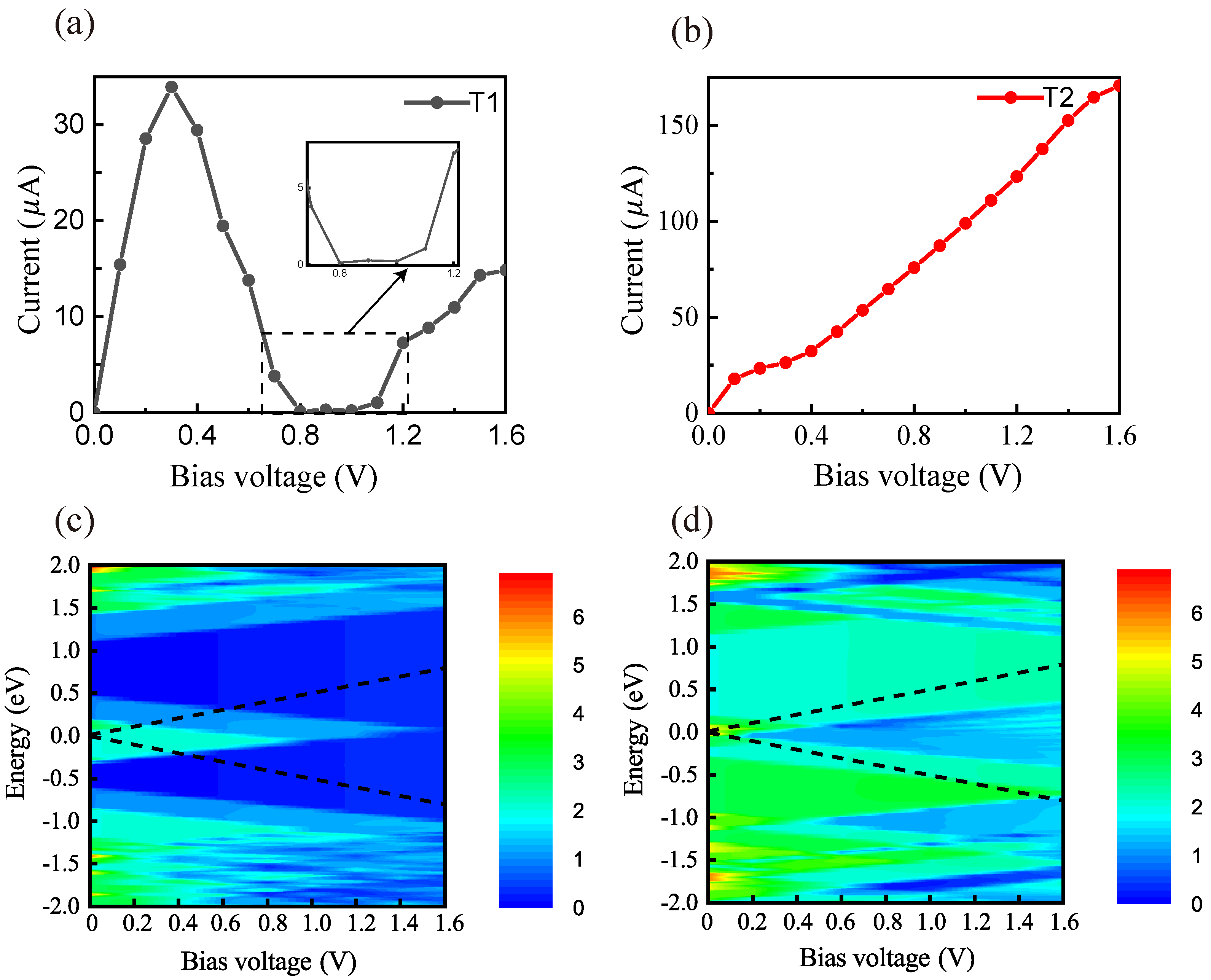
The considered model is shown in Figure 1 and consists of several single layers of green phosphorene repeated in the z-direction. It has been demonstrated that single-layer green phosphorene without hydrogen termination at the edges is a stable structure [38]. We consider two different edge morphologies of monolayer green phosphene: one is zigzag, and the other is whisker, which are labeled Type 1 and Type 2, respectively. Type 1 is the existing structure, and Type 2 is obtained by cutting on the basis of Type 1. The molecular device consists of three parts: the first part includes the left and right electrodes, the second part is the electrode extension region, and the third part is the central scattering region. In the simulation calculations, the central scattering region contains 60 phosphorus atoms. In the molecular device structure, We perform n-type doping on the left and right electrodes as well as the electrode extension region to generate a non-equilibrium state in the device system, with a doping concentration of 1 × 10 19 e / cm 3 . The doping concentration in our simulated device structure corresponds to doping only a few electrons at the scale of our device. During the device experiment, the device’s electrodes need to make contact with metal electrodes, which also leads to electron injection. This effectively simulates the realistic experimental environment. After geometric optimization, in Type 1, the bond lengths between adjacent phosphorus atoms are measured to be 2.23 Å and 2.26 Å, as shown in Figure 1a. In Type 2, the bond lengths between adjacent phosphorus atoms are 2.25 Å and 2.26 Å, as shown in Figure 1b. This bond length is basically the same as described in the literature [39]. The entire structure adopts an x-z coplanar configuration, with the transport direction along the z-direction.
We perform the geometric optimization and calculation of transport properties for Types 1 and 2, using the developed first-principles calculation software package (ATK) [40], which combines DFT with NEGF theory. In the calculations of the energy bands, we employ the Perdew–Burke–Ernzerhof (PBE) exchange-correlation functional within the generalized gradient approximation (GGA). The grid cutoff value for the electrostatic potential of 285 Ry is chosen, and the Fermi function is at a temperature of 300 K. A Monkhorst–Pack k-point grid of 1 × 1 × 285 was chosen for the calculations. The lattice parameters and atomic positions were fully relaxed, with energy and force convergence criteria set to 10 5 eV and 0.05 eV/Å, respectively. A vacuum spacing of at least 15 Å was added in the direction perpendicular to the electronic transport plane to avoid interactions caused by periodic boundary conditions. For Type 1 and Type 2, we employ the NEGF method to calculate their transmission eigenvalues spectra and current–voltage (I–V) curves. When a voltage is applied, the electrochemical potentials of the left and right electrodes move accordingly. The current at a specific bias voltage, V b , is obtained using the Landauer–Büttiker formula:
I ( V ) = 2 e h μ L μ R T ( E , V b ) [ f L ( E μ L ) f R ( E μ R ) ] d E ,
in this equation, μ L ( R ) = E F ± e V b / 2 represents the electrochemical potentials of the left and right electrodes, where the potential difference between the electrodes is equal to the bias voltage V b . f L ( E μ L ) and f R ( E μ R ) are the Fermi distribution functions of the left and right electrodes at equilibrium. T ( E , V b ) is the electron transmission probability function, and it is calculated using the retarded Green’s function G ( E , V b ) :
T ( E , V b ) = T r [ Γ L ( E , V b ) G ( E , V b ) Γ R ( E , V b ) G ( E , V b ) ] ,
in the above equation, Γ L ( R ) = i ( L ( R ) L ( R ) ) represents the broadening matrices of the left (right) electrode, where L ( R ) is the coupling self-energy between the semi-infinite left (right) electrode and the central region.

3. Results

Based on the above considerations, we calculate the band structures of the left and right electrodes of Types 1 and 2, as shown in Figure 2a,c, which exhibit metal abundance. Besides, we also calculate their partial state density and total state density, as shown in Figure 2b,d, where the solid red line represents the state density of the upper and lower edge atoms of Types 1 and 2, the blue line represents the state density of all phosphorus atoms except the edge atoms, and the black line represents the state density of all atoms. Near the Fermi level, whether in Type 1 or Type 2, the red line representing the density of states (DOS) is higher than the blue line. This indicates that the DOS contributed by the edge atoms is larger, and the electrons are more localized at the edge atoms. For Type 1, because the phosphorus atoms at the edge have only one unformed bond, Type 2 has two unformed bonds, resulting in a high local density of electrons at the edge of Type 2. As one can see from the red line in the figure, DOS of Type 1 is 35 eV 1 , while DOS of Type 2 reaches 67 eV 1 . From the observation of the band structure near the Fermi level in Figure 2a,c, we find that two energy bands in Type 1 passing through the Fermi level are distributed in the conduction band region near the Γ point, and in the valence band region near the Z point, while Type 2 has four bands close to the Fermi level, which is an important aspect. It must affect their response to strain and transport characteristics.
After discussing the electronic structure of Type 1 and Type 2, in order to verify their differences in electron transport caused by energy band structures, we construct electronic devices and analyze their transport characteristics. The current–voltage (I–V) curves calculated using the Landauer–Büttiker Formula (1) are shown in Figure 3a,b. The electron transport properties of the two devices with different edge morphology are obviously distinct. Among them, the current passing through Type 1 gradually increases with the bias, reaching a maximum value of 34 µA at the bias voltage of 0.3 V, and then, when the bias voltage increases, the current passing through Type 1 drops to the lowest value of 0.23 µA.
As can be seen from the illustration in Figure 3a, the minimum current of the device is not zero. In contrast, the current through Type 2 increases linearly as the bias voltage increases. The electron transport characteristics of the electronic devices also confirm our previous theoretical analysis. In order to more clearly compare the electron transport properties of the two systems, we calculated their transmission spectra under the bias window with Formula (2), and the transmission spectra of the two structures are shown in Figure 3c,d. From the transmission spectrum of Type 1, we find that the transmittance of Type 1 has always been at a high level and observe that the transmission coefficient below the Fermi level starts to drop from 0.3 V and then rises to about 1.0 V, which also explains the reason for the NDR. For Type 2, in the bias window, there is a large number of transmission values exceeding 1, and with the opening of the bias window, the transmission value also gradually increases, which results in the I–V curves maintaining a linear increase in current.
Next, we discuss the response of Type 1 to strain and the effect of this regulation on the NDR effect. We define the strain as ϵ = ( a a 0 ) / a 0 , where a and a 0 are the lattice constants of the strained and the unstrained structures, respectively. When a strain occurs in one direction, the other direction is relaxed. First of all, Figure 4a,c,e display the band structure diagram, DOS diagram, and zero-bias transmission spectrum diagram when the compressive strain is 2 % , 5 % , and 8 % on the Y-axis, respectively.
It can be seen from the Figure 4 that the energy bands of the three groups and their responses to transmission are different under different strain intensities. The energy band of the strain structure varies greatly compared with that of the original structure. We note that an energy band of the 2 % strain structure crosses the Fermi level at the Γ point, where the energy gap between the conduction band and the valence band is small and increases rapidly. The energy gap at the Γ becomes smaller when the compressive strain is 5 % and 8 % . Similarly, from the DOS diagram, we also show that the contribution of each atom to the total electron orbital is also different under different compressive strains. When the compressive strain is 2 % , the density of states at the Fermi level is 0. The DOS at Fermi level increases with the strain increase, and the peak value of 8 % compression strain at 0.5 eV is higher than that at 5 % compression strain. Besides, we note that the zero bias transmission spectra of three different strain degrees that their response to different strain degrees is corresponding to the band and DOS diagram. As can be seen from the figure, with the compression along the y direction, the transmission coefficient of the zero-bias transmission spectrum of several strain-configuration devices at the Fermi level exceeds 2, but the difference is that the transmission spectrum of the 5 % compression strain has a very high peak value at 0.4 eV, while the transmission spectrum of the 8 % compression strain has two high transmission coefficient peaks at this energy point. Therefore, we believe that the current transmission spectra of the device display distinct responses to different compressive strain degrees. Next, we calculate the transmission spectrum of the whole system under different bias voltages to verify this result.
We calculated the transmission spectra under different strain conditions using Formula (2). Figure 4b,d,f shows the transmission spectra with compression strains of 2 % , 5 % , and 8 % , respectively.The area between the two (black) dashed lines represents the bias window, with bias ranging from 0 to 1.6 V. As shown in Figure 4b, the transmittance of the device structure with a compression strain of 2 % is always at a low level. In the bias window, the area with a transmission coefficient greater than 1 appears before the bias of 0.7 V, but after 0.4 V, the area covered by the part with a transmission coefficient greater than 1 in the bias window gradually decreases, indicating that the peak current is at 0.4 V. For Figure 4d with a compression strain of 5 % , we note that the high transmission region appears before 0.5 V in the bias window. Unlike Figure 4b, most regions with a transmission coefficient greater than 1 appear between 0.5 V and 0.9 V, indicating that the current value of this part is higher than that of the structure with a compression strain of 2 % . For Figure 4f with a compression strain of 8 % , the peak transmission also appears at 0.4 V, and with the increase of bias, it also maintains a high transmission coefficient in most regions within the bias window.
From the transmission spectra of several structures, we obtained their I–V curves using Formula (1). As shown in Figure 5a, the variations in the I–V curves of different structures, represented by different colored lines, corresponded to the results we predicted from the transmittance spectra. First, we can clearly see that the peak current of the strain structure is significantly increased by about 15 µA compared with the original structure, and the current of these strain structures increases rapidly with the increase of bias voltage, reaching 0.4 V and then gradually decreases with the further increase of bias, and NDR effects emerge. In particular, the I–V curves of strain structures show different peak-to-valley current ratios. The peak-valley specific currents of ϵ y = 0.02 , ϵ y = 0.05 and ϵ y = 0.08 are 9.27 , 2.66 , and 1.86 , respectively. As shown in Figure 5b, we calculate DOS for several strain structures. Corresponding to the color of the I–V curve, the green line represents a device with a compressive strain of ϵ y = 0.02 , the red line represents a device with a compressive strain of ϵ y = 0.05 , and the blue line represents a device with a compressive strain of ϵ y = 0.08 . We observe that with the increase of compressive strain, the peak value of DOS near the Fermi level of the device gradually increases, and the peak value increases. This result is also mirrored by the I–V diagram of the device under different strain conditions analyzed in the figure.

4. Conclusions

In summary, in this study we investigated the current transport characteristics of two different edge morphologies of green phosphorus devices. Firstly, we discussed the distinct electronic and transport properties of the zigzag edge (Type 1) and whisker-like (Type 2) configurations. Secondly, it was shown that the I–V characteristics of Type 1 exhibited a NDR effect, while the current of Type 2 linearly increased with bias. Thirdly, we also discussed the current transport characteristics of the Type 1 configuration under strain modulation. Fourthly, from the perspectives of the band structure, the DOS, and the transmission spectra, we analyzed the physical reasons for the transport differences under different strain modulations in detail. Finally, different strain intensities proved to result in different peak-to-valley ratios of the current. These results provide effective avenues for exploring the influence of edge morphology on device transport and studying the response between strain and NDR effect. These results share a guiding significance for the design of electronic nano-devices made of two-dimensional green phosphorene.

Author Contributions

Conceptualization, S.L. and H.Y.; methodology, S.L. and H.Y.; software, S.L. and H.Y.; resources, H.Y.; writing—original draft preparation, S.L.; writing—review and editing, H.Y.; funding acquisition, H.Y. All authors have read and agreed to the published version of the manuscript.

Funding

This work was supported by the National Nature Science Foundation of China (Grant No. 12164023), the Yunnan Local College Applied Basic Research Projects (Grant No. 2017FH001-001), and the Yunnan Local College Applied Basic Research Projects (Grant No. 2023Y0882).

Institutional Review Board Statement

Not applicable.

Informed Consent Statement

Not applicable.

Data Availability Statement

The data presented in this study are available on request from the corresponding author by the reason that the data has not been made publicly available.

Conflicts of Interest

The authors declare no conflict of interest.

References

  1. Zhou, Y.; Zhang, D.; Zhang, J.; Ye, C.; Miao, X. Negative differential resistance behavior in phosphorus-doped armchair graphene nanoribbon junctions. J. Appl. Phys. 2014, 115, 073703. [Google Scholar] [CrossRef]
  2. Hong, X.K.; Kuang, Y.W.; Qian, C.; Tao, Y.M.; Yu, H.L.; Zhang, D.B.; Liu, Y.S.; Feng, J.F.; Yang, X.F.; Wang, X.F. Axisymmetric All-Carbon Devices with High-Spin Filter Efficiency, Large-Spin Rectifying, and Strong-Spin Negative Differential Resistance Properties. J. Phys. Chem. C 2015, 120, 668–676. [Google Scholar] [CrossRef]
  3. Wu, Q.; Liu, R.; Qiu, Z.; Li, D.; Li, J.; Wang, X.; Ding, G. Cr3X4 (X = Se, Te) monolayers as a new platform to realize robust spin filters, spin diodes and spin valves. Phys. Chem. Chem. Phys. 2022, 24, 24873–24880. [Google Scholar] [CrossRef]
  4. Dong, X.; Peng, Z.; Chen, T.; Xu, L.; Ma, Z.; Liu, G.; Cen, K.; Xu, Z.; Zhou, G. Electronic structures and transport properties of low-dimensional GaN nanoderivatives: A first-principles study. Appl. Surf. Sci. 2021, 561, 150038. [Google Scholar] [CrossRef]
  5. Huang, L.; Chen, S.Z.; Zeng, Y.J.; Wu, D.; Li, B.L.; Feng, Y.X.; Fan, Z.Q.; Tang, L.M.; Chen, K.Q. Switchable Spin Filters in Magnetic Molecular Junctions Based on Quantum Interference. Adv. Electron. Mater. 2020, 6, 2000689. [Google Scholar] [CrossRef]
  6. Luisier, M. Atomistic simulation of transport phenomena in nanoelectronic devices. Chem. Soc. Rev. 2014, 43, 4357–4367. [Google Scholar] [CrossRef]
  7. Zhou, Y.; Zheng, X.; Cheng, Z.-Q.; Chen, K.-Q. Current Superposition Law Realized in Molecular Devices Connected in Parallel. J. Phys. Chem. C 2019, 123, 10462–10468. [Google Scholar] [CrossRef]
  8. Chen, Q.; Zheng, X.; Jiang, P.; Zhou, Y.-H.; Zhang, L.; Zeng, Z. Electric field induced tunable half-metallicity in an A-type antiferromagnetic bilayer LaBr2. Phys. Rev. B 2022, 106, 245423. [Google Scholar] [CrossRef]
  9. He, X.; Chen, J.; Li, S.; Lin, M.; Wang, Y.; Zheng, Y.; Lu, H. The tunability of electronic and transport properties of InSe/MoSe2 van der Waals heterostructure: A first-principles study. Surf. Interfaces 2023, 36, 102634. [Google Scholar] [CrossRef]
  10. Wang, X.; Feng, Z.; Rong, J.; Zhang, Y.; Zhong, Y.; Feng, J.; Yu, X.; Zhan, Z. Planar net-τ: A new high-performance metallic carbon anode material for lithium-ion batteries. Carbon 2019, 142, 438–444. [Google Scholar] [CrossRef]
  11. Wang, Z.F.; Jin, K.-H.; Liu, F. Quantum spin Hall phase in 2D trigonal lattice. Nat. Commun. 2016, 7, 12746. [Google Scholar] [CrossRef] [PubMed]
  12. Li, X.; Wang, X.; Zhang, L.; Lee, S.; Dai, H. Chemically Derived, Ultrasmooth Graphene Nanoribbon Semiconductors. Science 2008, 319, 1229–1232. [Google Scholar] [CrossRef]
  13. Su, H.-P.; Shao, Z.-G. Lithium enhancing electronic transport properties of monolayer 6,6,12-graphyne from first principles. Surf. Interfaces 2021, 22, 100903. [Google Scholar] [CrossRef]
  14. Wu, Q.-H.; Zhao, P.; Liu, H.-Y.; Liu, D.-S.; Chen, G. Odd–even dependence of rectifying behavior in carbon chains modified diphenyl–dimethyl molecule. Chem. Phys. Lett. 2014, 62, 605–606. [Google Scholar] [CrossRef]
  15. Wu, X.; Xiao, S.; Quan, J.; Tian, C.; Gao, G. Perylene-based molecular device: Multifunctional spintronic and spin caloritronic applications. Phys. Chem. Chem. Phys. 2023, 25, 7354–7365. [Google Scholar] [CrossRef]
  16. Kinikar, A.; Phanindra Sai, T.; Bhattacharyya, S.; Agarwala, A.; Biswas, T.; Sarker, S.K.; Krishnamurthy, H.R.; Jain, M.; Shenoy, V.B.; Ghosh, A. Quantized edge modes in atomic-scale point contacts in graphene. Nat. Nanotechnol. 2017, 12, 564–568. [Google Scholar] [CrossRef]
  17. Wu, Q.; Shen, L.; Yang, M.; Cai, Y.; Huang, Z.; Feng, Y.P. Electronic and transport properties of phosphorene nanoribbons. Phys. Rev. B 2015, 92, 035436. [Google Scholar] [CrossRef]
  18. Stegner, A.R.; Pereira, R.N.; Klein, K.; Lechner, R.; Dietmueller, R.; Brandt, M.S.; Stutzmann, M.; Wiggers, H. Electronic Transport in Phosphorus-Doped Silicon Nanocrystal Networks. Phys. Rev. Lett. 2008, 100, 026803. [Google Scholar] [CrossRef]
  19. Jia, C.; Cao, L.; Zhou, X.; Zhou, B.; Zhou, G. Low-bias negative differential resistance in junction of a benzene between zigzag-edged phosphorene nanoribbons. J. Phys. Condens. Matter 2018, 30, 265301. [Google Scholar] [CrossRef] [PubMed]
  20. Zheng, C.; Wu, K.; Jiang, K.; Yao, K.; Zhu, S.; Lu, Y. Perfect spin filtering effect, tunnel magnetoresistance and thermoelectric effect in metals-adsorbed blue phosphorene nanoribbons. Physica B 2022, 626, 413580. [Google Scholar] [CrossRef]
  21. Han, W.H.; Kim, S.; Lee, I.-H.; Chang, K.J. Prediction of Green Phosphorus with Tunable Direct Band Gap and High Mobility. J. Phys. Chem. Lett. 2017, 8, 4627–4632. [Google Scholar] [CrossRef]
  22. Qu, H.; Guo, S.; Zhou, W.; Wu, Z.; Cao, J.; Li, Z.; Zeng, H.; Zhang, S. Enhanced interband tunneling in two-dimensional tunneling transistors through anisotropic energy dispersion. Phys. Rev. B 2022, 105, 075413. [Google Scholar] [CrossRef]
  23. Liu, C.; Fu, B.; Yin, H.; Zhang, G.; Dong, C. Strain-tunable magnetism and nodal loops in monolayer MnB. Appl. Phys. Lett. 2020, 117, 103101. [Google Scholar] [CrossRef]
  24. Rezania, H.; Nourian, E.; Abdi, M.; Astinchap, B. Strain and magnetic field effects on the electronic and transport properties of γ-graphyne. RSC Adv. 2023, 13, 7988–7999. [Google Scholar] [CrossRef]
  25. Roldán, R.; Castellanos-Gomez, A.; Cappelluti, E.; Guinea, F. Strain engineering in semiconducting two-dimensional crystals. J. Phys. Condens. Matter 2015, 27, 313201. [Google Scholar] [CrossRef]
  26. Chen, Q.-Y. First-principles study on superconductive properties of compressive strain-engineered cryogenic superconducting heavy metal lead (Pb). Commun. Theor. Phys. 2021, 73, 035703. [Google Scholar] [CrossRef]
  27. Yang, N.; Chen, Q.; Xu, Y.; Luo, J.; Yang, H.; Jin, G. Strain-modulated electronic transport in two-dimensional carbon allotropes. AIP Adv. 2022, 12, 045102. [Google Scholar] [CrossRef]
  28. Ren, Y.; Cheng, F.; Zhou, X.-Y.; Chang, K.; Zhou, G.-H. Tunable mechanical, electronic and magnetic properties of monolayer C3N nanoribbons by external fields. Carbon 2019, 143, 14–20. [Google Scholar] [CrossRef]
  29. Ren, Y.; Liu, P.; Zhou, B.; Zhou, X.; Zhou, G. Crystallographic Characterization of Black Phosphorene and its Application in Nanostructures. Phys. Rev. Appl. 2019, 12, 064025. [Google Scholar] [CrossRef]
  30. Chen, J.; Zhang, Z.; Lu, H. Structure design and properties investigation of Bi2O2Se/graphene van der Waals heterojunction from first-principles study. Surf. Interfaces 2022, 33, 102289. [Google Scholar] [CrossRef]
  31. Brandbyge, M.; Mozos, J.L.; Ordejón, P.; Taylor, J.; Stokbro, K. Density-functional method for nonequilibrium electron transport. Phys. Rev. B 2022, 65, 165401. [Google Scholar] [CrossRef]
  32. Zhu, Y.; Li, H.; Chen, T.; Liu, D.; Zhou, Q. Investigation of the electronic and magnetic properties of low-dimensional FeCl2 derivatives by first-principles calculations. Vacuum 2020, 182, 109694. [Google Scholar] [CrossRef]
  33. Li, Y.-F.; Zhao, P.; Xu, Z.; Chen, G. Effect of linkage mode on the spin-polarized transport of a TPV radical-based molecular device. Chem. Phys. Lett. 2022, 794, 139515. [Google Scholar] [CrossRef]
  34. Poljak, M.; Suligoj, T. Immunity of electronic and transport properties of phosphorene nanoribbons to edge defects. Nano Res. 2016, 9, 1723–1734. [Google Scholar] [CrossRef]
  35. Zhang, W.; Basaran, C.; Ragab, T. Impact of geometry on transport properties of armchair graphene nanoribbon heterojunction. Carbon 2017, 124, 422–428. [Google Scholar] [CrossRef]
  36. Wu, Q.; Ang, L.K. Giant tunneling magnetoresistance in atomically thin VSi2N4/MoSi2N4/VSi2N4 magnetic tunnel junction. Appl. Phys. Lett. 2022, 120, 022401. [Google Scholar] [CrossRef]
  37. Chen, Q.-Y.; Liu, M.-Y.; Cao, C.; He, Y. Strain-tunable electronic and optical properties of novel anisotropic green phosphorene: A first-principles study. Nanotechnology 2019, 30, 335710. [Google Scholar] [CrossRef]
  38. Han, X.; Stewart, H.M.; Shevlin, S.A.; Catlow, C.R.A.; Guo, Z.X. Strain and Orientation Modulated Bandgaps and Effective Masses of Phosphorene Nanoribbons. Nano Lett. 2014, 14, 4607–4614. [Google Scholar] [CrossRef]
  39. Singsen, S.; Watwiangkham, A.; Ngamwongwan, L.; Fongkaew, I.; Jungthawan, S.; Suthirakun, S. Defect Engineering of Green Phosphorene Nanosheets for Detecting Volatile Organic Compounds: A Computational Approach. ACS Appl. Nano Mater. 2023, 6, 1496–1506. [Google Scholar] [CrossRef]
  40. QuantumATK Version T-2022.03, Synopsys QuantumATK. Available online: http://www.quantumwise.com (accessed on 1 December 2023).
Figure 1. (a) Zigzag edge morphology of green phosphorus. (b) Whisker edge morphology of green phosphorus. N-type doping is carried out within the green box, which includes electrodes and electrode extension regions, with a doping concentration of 1 × 10 19 e / cm 3 .
Crystals 14 00239 g001
Figure 2. (a,c) Band structures of the left electrode. (b,d) Total density of states and partial density of states for Type 1 and Type 2, respectively.
Crystals 14 00239 g002
Figure 3. (a,b) I–V curves. (c,d) Transmission spectra for Type 1 and Type 2, respectively. The black dashed lines indicate the bias window.
Crystals 14 00239 g003
Figure 4. (a,c,e) Band structure on the left panel, DOS on the middle panel, and zero bias transmission spectra for the left electrode of Type 1 on the right panel, when the applied strain is ϵ y = 0.02 , ϵ y = 0.05 , and ϵ y = 0.08 , respectively. The red dashed line represents the Fermi level. (b,d,f) The transmission spectra of Type 1 at strains of ϵ y = 0.02 , ϵ y = 0.05 , and ϵ y = 0.08 , respectively. The black dashed line represents the bias window.
Crystals 14 00239 g004
Figure 5. (a) I–V curves of Type 1 under different strain conditions. (b) DOS of the device under different strain conditions.
Crystals 14 00239 g005
Disclaimer/Publisher’s Note: The statements, opinions and data contained in all publications are solely those of the individual author(s) and contributor(s) and not of MDPI and/or the editor(s). MDPI and/or the editor(s) disclaim responsibility for any injury to people or property resulting from any ideas, methods, instructions or products referred to in the content.

