Article

Analysis of the Effect of Copper Doping on the Optoelectronic Properties of Indium Oxide Thin Films and the Thermoelectric Properties of an In2O3/Pt Thermocouple

Department of Electronic Engineering, Xi’an University of Technology, Xi’an 710048, China
*
Authors to whom correspondence should be addressed.
Crystals 2024, 14(1), 78; https://doi.org/10.3390/cryst14010078
Submission received: 27 December 2023 / Revised: 9 January 2024 / Accepted: 11 January 2024 / Published: 13 January 2024
(This article belongs to the Special Issue Wide-Bandgap Semiconductor Materials, Devices and Systems)

Abstract

:
The detection and real-time monitoring of temperature parameters are important, and indium oxide-based thin film thermocouples can be integrated on the surface of heaters because they operate normally under harsh conditions and provide accurate online temperature monitoring. The higher stability and appropriate optical and electrical properties of In2O3 make it very suitable as an electrode material for thermocouple sensors. This work demonstrates that copper doping can alter the optical and electrical properties of In2O3 films and regulate the output performance of thermocouples. Copper-doped In2O3 thin films were prepared using the magnetron co-sputtering method. The doping concentration of Cu was controlled using direct current (DC) power. An In2O3/Pt thermocouple sensor was prepared, and the optoelectronic and thermocouple properties were adjusted by changing the copper doping content. The thickness valve of the thin film sample was 300 nm. The results of the X-ray diffraction suggested that the structure of the doped In2O3 thin films was cubic. The results of the energy-dispersive X-ray analysis revealed that Cu was doped into the In2O3 thin films. All deposited films were n-type semiconductor materials according to Hall effect testing. The 4.09 at% Cu-doped thin films possessed the highest resistivity (30.2 × 10⁻³ Ω·cm), a larger carrier concentration (3.72 × 1020 cm−3), and the lowest carrier mobility (0.56 cm2V−1s−1). The optical band gap decreased from 3.76 to 2.71 eV with an increase in the doping concentration, and the transmittance of the film significantly reduced. When the DC power was increased, the variation range of Seebeck coefficient for the In2O3/Pt thermocouple was 152.1–170.5 μV/°C, and the range of thermal output value was 91.4–102.4 mV.

1. Introduction

Transparent conductive oxide (TCO) thin films have a significant research value and are widely used in many applications such as solar cells, display devices, photoelectronic devices, and touchscreens [1,2,3,4]. Metal oxides commonly used in TCO thin film systems include cadmium oxide (CdO), zinc oxide (ZnO), tin oxide (SnO2), and indium oxide (In2O3) [5,6,7,8]. The demand for TCO thin films has increased over the last few years with the rapid development of various devices. In2O3 is an n-type semiconductor. Its band gap is 3.5–3.7 eV, and it is widely used in transparent conducting electrodes, solar cells, displays, and photoelectric sensors [9,10].
The electrical and optical properties of an In2O3 thin film can be improved by doping metal elements such as Sn, Cr, Mo, Ce, Sb, Li, Zn, and Cu [11,12,13,14,15,16,17,18,19,20,21,22]. Pramod et al. prepared Sb-doped In2O3 films [18]; the highest optical transmittance was obtained at 1.5 at.%, and the doping amount was able to change the optical band gap of the In2O3 films. Ahmed et al. prepared (In1−xCrx)2O3 thin films under different Cr doping concentrations [16]. As the Cr doping concentration increased, the films preferentially oriented along the (222) direction under different component conditions, and the optical band gap value increased from 3.21 eV to 3.46 eV. Shi et al. prepared Ce-doped In2O3 thin films under low-temperature conditions using radio frequency reactions [17]. According to an electrical performance test, the carrier concentration of the films reached 2.1 × 1020 cm−3, and the highest mobility obtained was 153.7 cm2/Vs. Wang et al. prepared In2O3 thin films with a resistivity of 3.76 × 10⁻⁴ Ω·cm by doping Hf [18]. Their study revealed that the Hall mobility could reach 79.6 cm2/Vs, and the average transmittance of the thin film could reach 83% in the range of 300–1500 nm. Indium–gallium–zinc oxide (IGTO) thin films on flexible substrates were developed by Kang et al. using co-doping with Ga and Ti when the oxygen flow was zero [19]. The sheet resistance of IGTO was 39.3 Ω/sq, and the transmittance of the IGTO film reached 86.96%. Kaleemulla et al. prepared Mo-doped In2O3 thin films on glass substrates using the activated reactive evaporation method [20]. The films synthesized at a Mo doping level of 3% and a substrate temperature of 573 K. The electrical resistivity achieved a minimum value of 5.2 × 10⁻⁴ Ω·cm, the average optical transmittance of the films reached 90%, and the band gap was 3.68 eV. Fan Ye et al. prepared Cu-doped In2O3 using the reactive DC magnetron sputtering method [21]. The results revealed that Cu doping could significantly alter the electrical and optical properties of thin films. The resistivity of the doped In2O3 thin films reached 1.82 Ω·cm, and the minimum optical band gap could be reduced to 3.70 eV. Otto J. Gregory constructed Cu-In-O thin films [22], and found that in a composition of 40.0 atom % indium, thin films can transition from p-type to n-type conduction.
The common methods used In the preparation of In2O3 thin films include sol–gel, pulsed laser deposition (PLD), metal–organic chemical vapor deposition (MOCVD), and magnetron sputtering [23,24,25,26,27,28]. Gupta et al. prepared Gd-doped In2O3 films on quartz substrates using the PLD method [23]. Under a vacuum and 600 °C growth conditions, high-conductivity indium oxide thin films were obtained with a carrier concentration of 1.74 × 1020 cm−3, a resistivity of 2.80 × 10⁻⁴ Ω·cm, and a mobility of 1.28 × 102 cm2V−1s−1. Sanchez et al. prepared In2O3 thin films on the c-axis of sapphire substrates using a low-temperature sol–gel method [24]. They observed an increase in the carrier concentration of the films to 2.45 × 1019 cm−3, with a resistivity of 3.5 Ω·cm noted after heat treatment at 700 °C. Baqiah et al. prepared In2O3 thin films using the CVD method, with InCl3·4H2O as the initial raw material [25]. The resistivity of the films in their study reached 1.458 × 10⁻² V·cm at a deposition temperature of 720 K. According to Du et al., the resistivity of In2O3 thin films prepared using the MOCVD method could reach 1.458 × 10⁻² V·cm at a deposition temperature of 720 K [26]. Compared with other preparation methods, the magnetron sputtering method is widely used in certain areas because of its superiority in terms of uniformly deposited films, its high purity, and wide application to target materials. Cho used a radio frequency reaction method to prepare In2O3 thin films on target materials [27]. The films were preferentially oriented along the (222) and (400) directions, and the average transmittance reached 88.6% in the range of 370–1100 nm. Yuan et al. prepared In2O3 thin films on amorphous glass using the magnetron sputtering method [28]. A high field-effect mobility of thin film transistors was obtained by optimizing the annealing process.
Due to its excellent stability and significant thermoelectric potential output under high-temperature conditions, indium oxide is often used as an electrode material for high-temperature thermocouples [29,30,31]. Its thermoelectric output characteristics can be adjusted via doping with indium oxide thin films. Liu Dan et al. prepared indium oxide thin films using radio-frequency magnetron sputtering, and constructed La0.8Sr0.2CrO3/In2O3 thermocouples [32]. The thermoelectric potential output reached 305.8 μV/°C at 1100 °C. By doping Sn to adjust the thermoelectric output characteristics of indium oxide thin films, Xiaohui Zhao et al. used magnetron sputtering to construct ITO/Pt thin film thermocouples on nickel alloy substrates. A high-temperature tolerance of up to 1100 °C was recorded [33]. To improve the stability of thermocouples, Zhongkai Zhang et al. constructed In1.35ZnO2.11/In2O3 thermocouples using screen-printing technology. This resulted in a thermoelectric potential output of 39.8 μV/°C at 1500 °C. The drift rate was 0.84 °C/h [34]. Zhao X.H et al. prepared ITON-InON ceramic thin film thermocouples [35]; the samples were heated at 1000 °C for 5 h in a nitrogen-rich atmosphere and 5 h in air, respectively, which improved the output stability of the thermocouple, and the average Seebeck reached 64.7 μV/°C. Liu et al. treated indium oxide thin films at a high temperature of 1150 °C for 10 h, and the In2O3/ITO thermocouple was able to output normally [36].
In this study, we prepared copper-doped thin films using the co-sputtering method, achieved indium oxide thin films with adjustable transmittance and electrical properties, and obtained thin film thermocouples with an adjustable output thermal voltage. We investigated the electrical and optical properties of undoped In2O3 and Cu-doped In2O3 thin films, the effect of the Cu ion concentration on the microstructure, and the electrical and optical properties of In2O3. The thermoelectric properties of the In2O3/Pt thermocouple were systematically characterized.

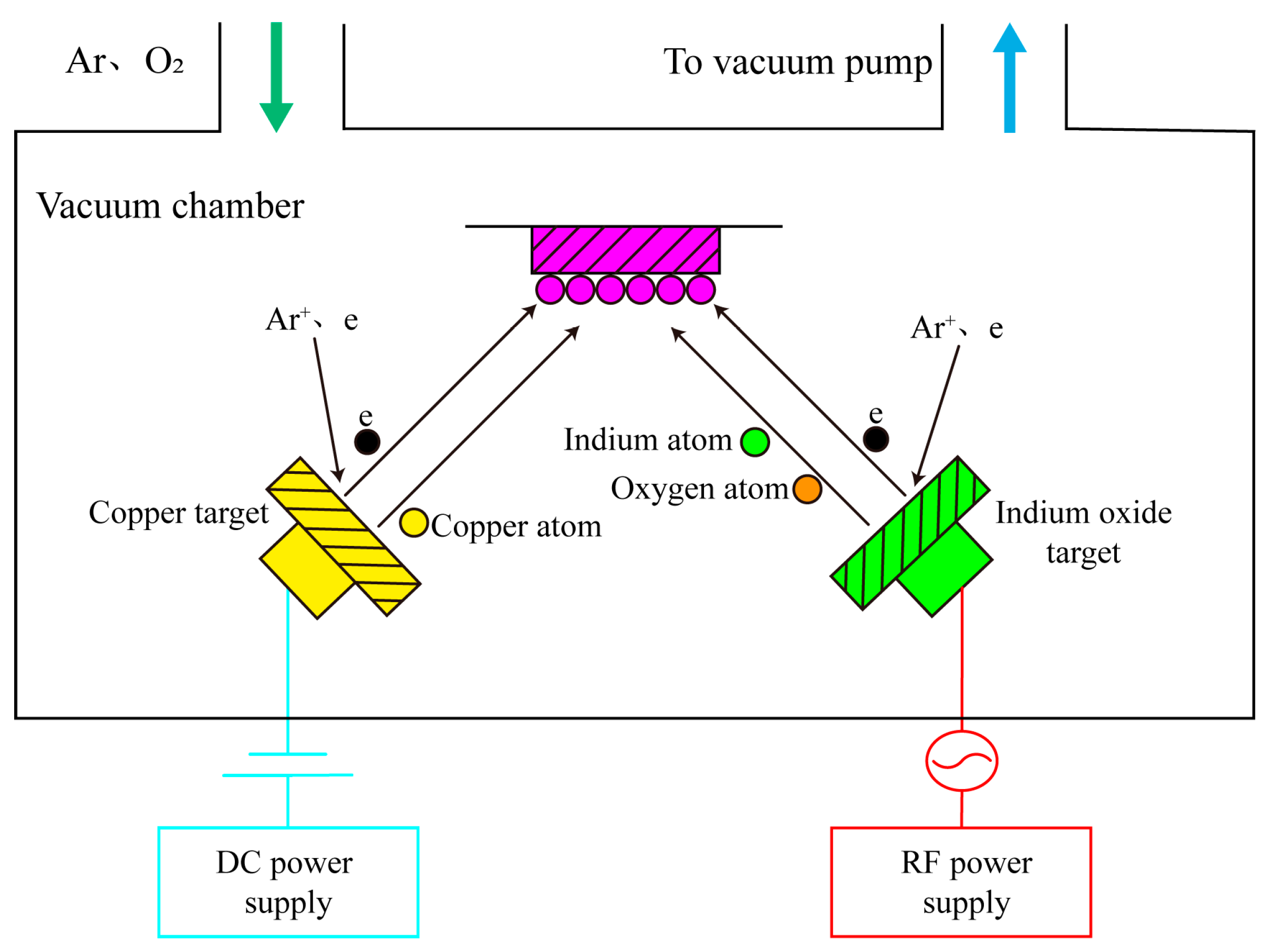
2. Materials and Methods

In2O3 was created on quartz substrates with different concentrations of copper doping using magnetron co-sputtering equipment (SP3-80C, Chuangshiweina Technology Co., Beijing China). We altered the direct current (DC) sputtering power during the preparation process to obtain the different Cu-doping concentrations. The samples of In2O3 with different Cu-doping concentrations (sputtered by DC power) were prepared at room temperature using DC sputtering power supplies of 10 W, 15 W, 20 W, and 25 W. The diameter of all In2O3 and Cu targets was 80 mm, and the purity of both the In2O3 and Cu targets was 99.99%. The In2O3 target was set at a sputtering power of 100 W using a radio-frequency power supply throughout the entire sputtering process. Before sputtering, substrates with a size of 10 mm × 10 mm and a thickness of 0.7 mm were cleaned for 15 min in an ultrasonic bath using alcohol and acetone separately. These were then repeatedly rinsed using deionized water and dried with a high-pressure nitrogen gun. The base pressure of the chamber was 6.0 × 10⁻⁴ Pa, and the sputtering pressure was 1.5 Pa. The substrates were rotated at 14 revolutions per minute (rpm) during the deposition process. The oxygen-to-argon ratio was set at 1:6, the argon gas flow rate was maintained at 60 standard cubic centimeters per minute (sccm), and the sputtering time was set at 3 h. After the sputtering process, the thin films were annealed in a high-temperature atmosphere furnace (OTF-1200X; MTI, Hefei, China) at 500 °C in an air atmosphere for 1 h. The parameters of the indium oxide and copper targets during co-sputtering are presented in Table 1, and the magnetron co-sputtering of In2O3 doped with Cu is diagrammatically represented in Figure 1.
The pure and doped In2O3 thin films were tested using an X-ray diffractometer (XRD) (Ultima IV, Rigaku, Hitachi, Tokyo, Japan). The surface images and EDX patterns of the thin film samples were determined using an SEM (Quanta 250, FEI, Hillsboro, OR, USA) equipped with an energy-dispersive spectrometer. The surface topography of the thin films was characterized by an AFM (Dimension Icon, Bruker, Billerica, MA, USA). The electrical and optical properties of the In2O3 thin films were investigated using a Hall effect testing system (CH300, CH-Magnetoelectricity Technology, Beijing, China) and an ultraviolet-visible spectrophotometer (Lamda950, PerkinElmer, Waltham, MA, USA), respectively.
To obtain the Seebeck coefficient of the pure and doped In2O3/Pt thermocouples, all of the films were fabricated (Figure 2). The length, width, and thickness of the quartz substrate were 10 cm, 10 mm, and 1.5 mm, respectively. After the deposition of In2O3 and Pt thin films, an In2O3 thin film with a width of 2.5 mm and a length of 9.5 cm was obtained. The Pt electrode was 2.5 mm, with a length of 9.5 cm. The overlapping area of the two electrodes was 2.5 mm × 2.5 mm. The preparation process is presented in Figure 3. First, pure and Cu-doped In2O3 thin films were fabricated using the co-sputtering method and a stainless steel metal mask to form an indium oxide electrode pattern. Second, the pure and Cu-doped In2O3 thin films were annealed in an air atmosphere at 500 °C for 1 h. Third, the Pt electrode was obtained using a sputtering system (JPG560, SKY Technology Development Co., Ltd., China) and a metal mask to form a Pt electrode pattern. The hot-end overlap area was 2.5 mm × 2.5 mm. The Pt target had a diameter of 4 inches, and the thickness was 4 mm. The instrumental settings of the sputtering process during the formation of the Pt electrode were a sputtering pressure of 0.5 Pa, a sputtering power of 100 W, and an argon flow rate of 80 sccm. The thickness of the obtained Pt thin film was approximately 300 nm.
As presented in Figure 4, the Seebeck coefficient and thermal voltage test system mainly consisted of one heating furnace, one voltmeter, two thermometers, and one cooling plate. A Nabertherm high-temperature heating furnace (LHT 2-17, Nabertherm, Lilienthal, Germany) was adapted to heat the hot end of the sample. The measurement range was set from room temperature to 600 °C, and the length of the K-type thermocouple was 20 cm. This was inserted into the high-temperature furnace to test the temperature of the hot end of the sample. Alumina foam transfer and high-temperature asbestos material were used between the hot and cold ends to insulate the treatment. The hot end of the film sample was pushed into the heating furnace to obtain the high-temperature difference between the two ends. An alumina foam brick was used as insulation material for the furnace door. A voltmeter was used to measure the output voltage of the cold end. Standard K-type thermocouples were used to measure the temperature of the hot and cold ends. The cold end was cooled by circulating water throughout the whole process, and the voltmeter was used to display the value of the thermal voltage.

3. Results

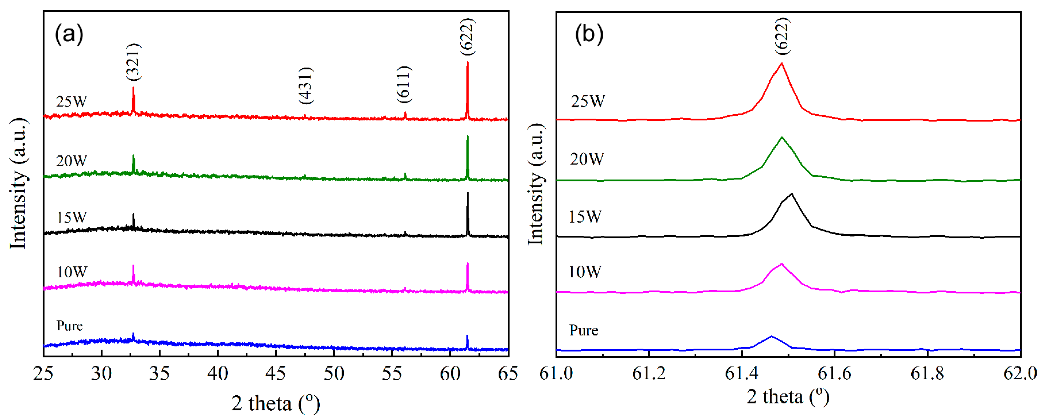
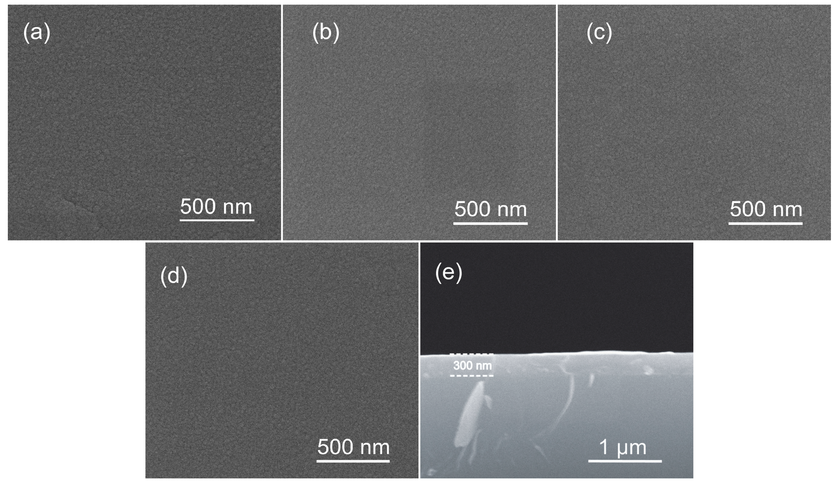
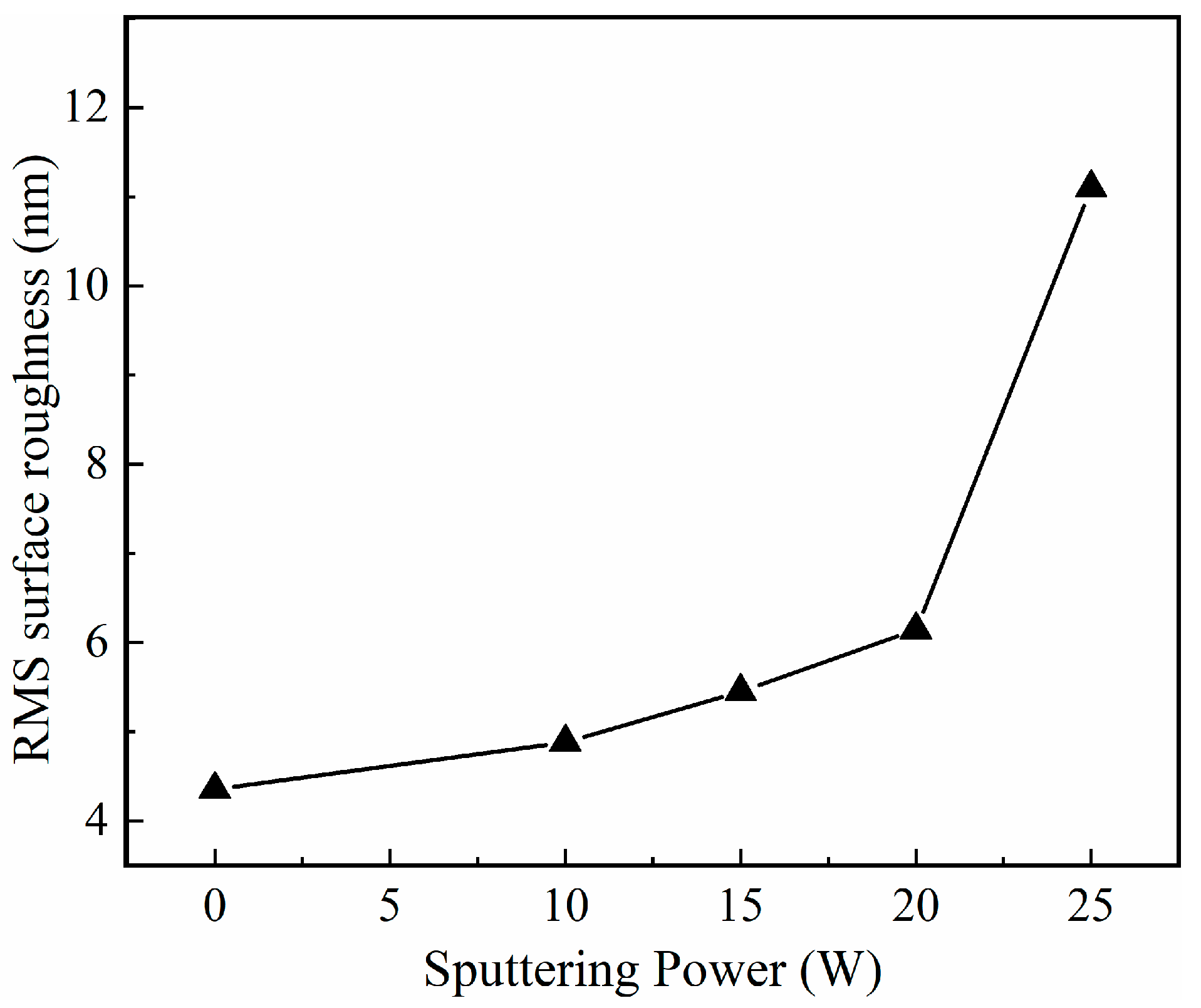
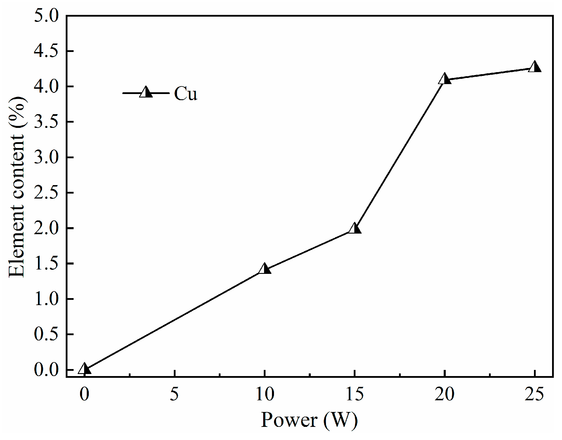
3.1. Microstructure and Other Physical Characteristics of Cu-Doped In2O3 Thin Films

The phase structure of the prepared thin film samples was determined using the XRD patterns obtained from 25° to 65°, with a 0.15418 nm wavelength of Cu K-alpha radiation. As demonstrated in Figure 5a, the cubic phase of In2O3 was observed in all thin film samples, and the space group was Ia 3 ¯ . No other peaks were observed, which implied that Cu doping had not added impurities, and that Cu was well incorporated into the lattice of the cubic In2O3 and had replaced the In atom. However, two new crystal phases with peaks of (431) and (611) simultaneously appeared. Figure 5b demonstrates the gradual shift in the peak (622) orientation of the doped thin film sample with an increase in the doping concentration. A similar observation was reported by Ye et al. [21]. The atomic radius of Cu is smaller than that of an In crystal; the substitution of smaller Cu for larger In could have changed the phase structure of the crystal, thereby shifting the corresponding diffraction peaks [37].
Figure 6 presents the crystal size values of the Cu-doped In2O3 films obtained using different DC sputtering powers. The grain size was estimated according to the Scherrer formula [38] (Equation (1)):
D = 0.9 λ / β cos θ
where λ is the X-ray wavelength, θ is the Bragg diffraction angle, and β is the full width at half maximum of the (622) peak. The increase in the DC sputtering power increased the full width at half maximum (FWHM) of the Cu-doped In2O3 films. The size of the crystallite increased from 17.1 nm to 38.9 nm when the DC sputtering power increased from 0 W to 25 W. The maximum value was obtained at DC 25 W. This was mainly attributed to the increase in the sputtering power and the increased number of grain boundary defects.
Figure 7a shows the the surface topography of unannealed pure film, and Figure 7b–d present the surface topography of the Cu-doped In2O3 thin film samples under 0 W, 15 W, and 25 W of DC power, respectively. Figure 7b–d reveal that the surface of the film was uniform. A distinct variation in the grain size was absent with an increase in the doping concentration. As presented in Figure 7e, the thickness of the prepared thin film sample was 300 nm. Figure 8 presents the AFM images at different DC sputtering powers; the effects of the Cu-doping concentration on the structural and surface morphology properties of the Cu-doped In2O3 thin films can clearly be observed. The Cu concentration evidently influenced the surface morphology of the Cu-doped In2O3 thin films. As the DC sputtering power increased, the grain size increased. This was the same trend of change as calculated from the XRD results. Figure 9 presents the surface roughness. The root mean square (RMS) increased from 4.3 nm to 11.1 nm as the DC sputtering power increased from 0 W to 25 W.
An energy-dispersive X-ray (EDX) analysis was used to further study the element types and contents of the prepared thin films. The EDX patterns of all samples prepared at DC sputtering powers from 0 W to 25 W are presented in Figure 10. The EDX data clearly demonstrate that the Cu doped into In2O3, and that there was a significant increase in the Cu content with an increase in the sputtering power from 0 W to 25 W. This could be attributed to the participation of Cu in an efficient substitution for indium (In) atoms. The calculated contents of Cu were 1.41%, 1.98%, 4.09%, and 4.26% for the thin film samples prepared at sputtering powers of 10 W, 15 W, 20 W, and 25 W, respectively (Figure 11).

3.2. Electrical Properties of Cu-Doped In2O3 Thin Films

The resistivity (ρ), carrier concentration (n), and mobility (μ) of all prepared thin film samples were determined using a Hall effect meter at room temperature, and are presented in Figure 12. The Hall effect measurement confirmed that the introduction of Cu did not change the n-type semiconducting behavior of the In2O3 films. When the sputtering power increased to 15 W, the resistivity also increased from 1.85 × 10⁻³ Ω·cm to 5.17 × 10⁻³ Ω·cm. The carrier concentration remained almost unchanged (15.3 × 1018 cm−3) between 0 W and 15 W DC sputtering powers. At a DC sputtering power of 20 W, relatively large changes in resistivity, carrier concentration, and mobility occurred; the values reached were 30.4 × 10⁻³ Ω·cm, 3.72 × 1020 cm−3, and 0.56 cm2V−1s−1, respectively. The change in the carrier concentration could have occurred for two reasons. It may have been due to the decrease in the band gap of the thin films causing a greater migration of carriers to the conduction band, thereby increasing the carrier concentration. The other reason may have been that the doping of the acceptor Cu could have generated holes to compensate for a negative charge [39,40]. The mobility tended to significantly decrease with an increase in the doping concentration.

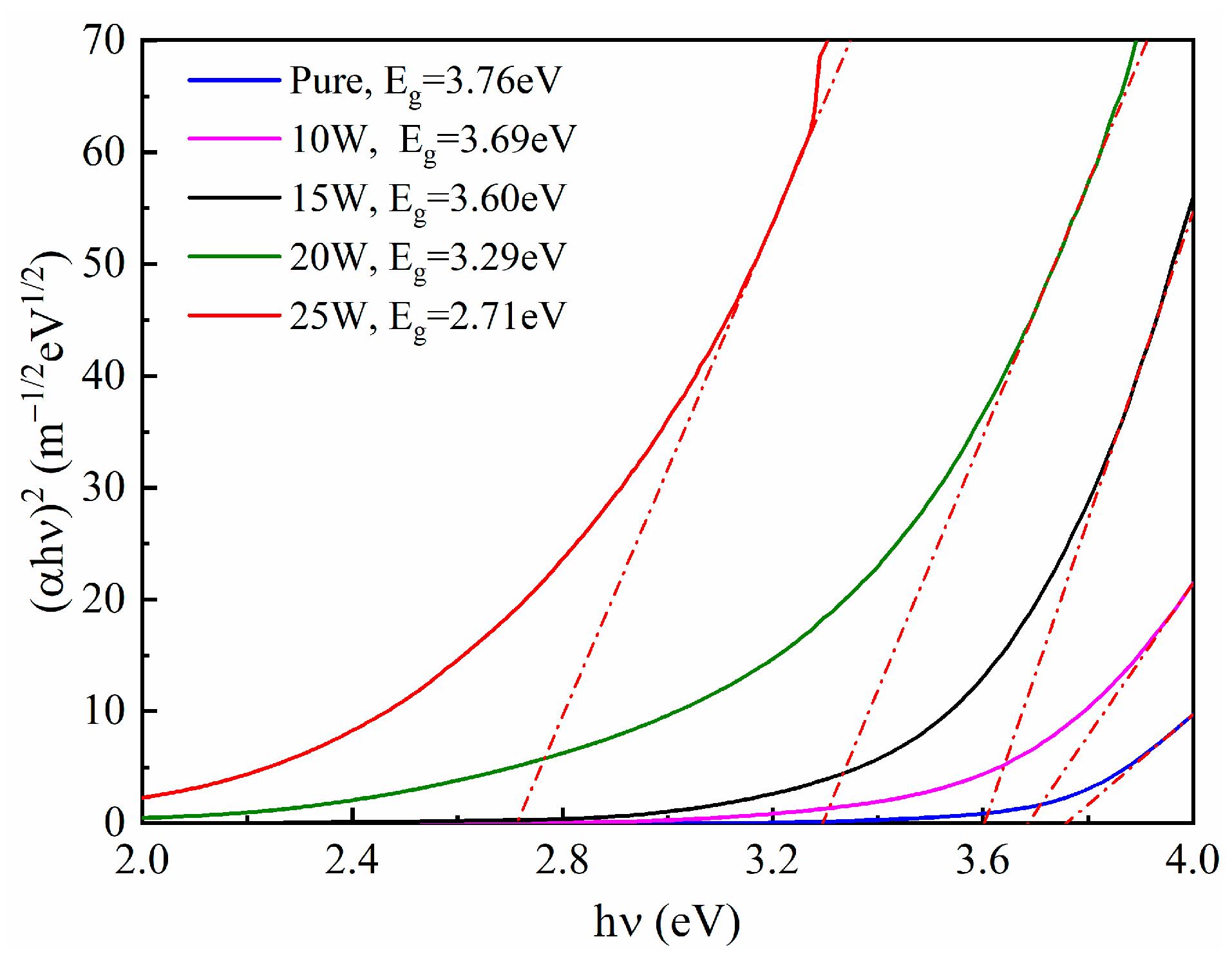
3.3. Optical Properties of Cu-Doped In2O3 Thin Films

The transmittance spectra of the Cu-doped In2O3 films are presented in Figure 13. A clear decrease in transmittance in the visible light region was observed as the Cu sputter power increased from 0 W to 25 W. The average transmittance revealed an overall downward trend. The pure In2O3 sample was 96% and the doping concentration under 10 W DC power was 85%, whereas the doping concentration decreased to 4.2% under a DC power of 25 W. Consequently, the doping concentration of Cu should not be too high during the preparation of Cu-doped In2O3 films.
The optical band gap is an important parameter when studying film properties. The optical band gap of the prepared thin film samples was determined to understand the influence of the doping concentration. The optical band gap was calculated using Equation (2) [41]:
α h ν 2 = A ( h ν E g )
where hv is the photon energy. The value of A depends on the direct or indirect band gap. α is the absorption coefficient, which can be determined using a formula that ignores the reflection of light on the film (Equation (3)) [42]:
α = ln 1 T / d
where d is the thickness of the film (the thickness value was 300 nm) and T is the transmission of the film (as demonstrated in Figure 12). The plot of (αhv)2 vs. hv can then be obtained (as presented in Figure 13) by extending the linear section of the curve to the x-axis. The optical band gap can then be determined from the intersection. As presented in Figure 14, the band gap (3.76 eV) obtained for the undoped sample was very close to the values reported in the literature [42] and the doped thin film samples revealed a decrease in the band gap with an increase in the Cu content. Several studies have observed that adding an element to an oxide can narrow the energy band gap of the doped material [43]. Our results also revealed a narrowing of the forbidden band of In2O3 from doping with Cu.

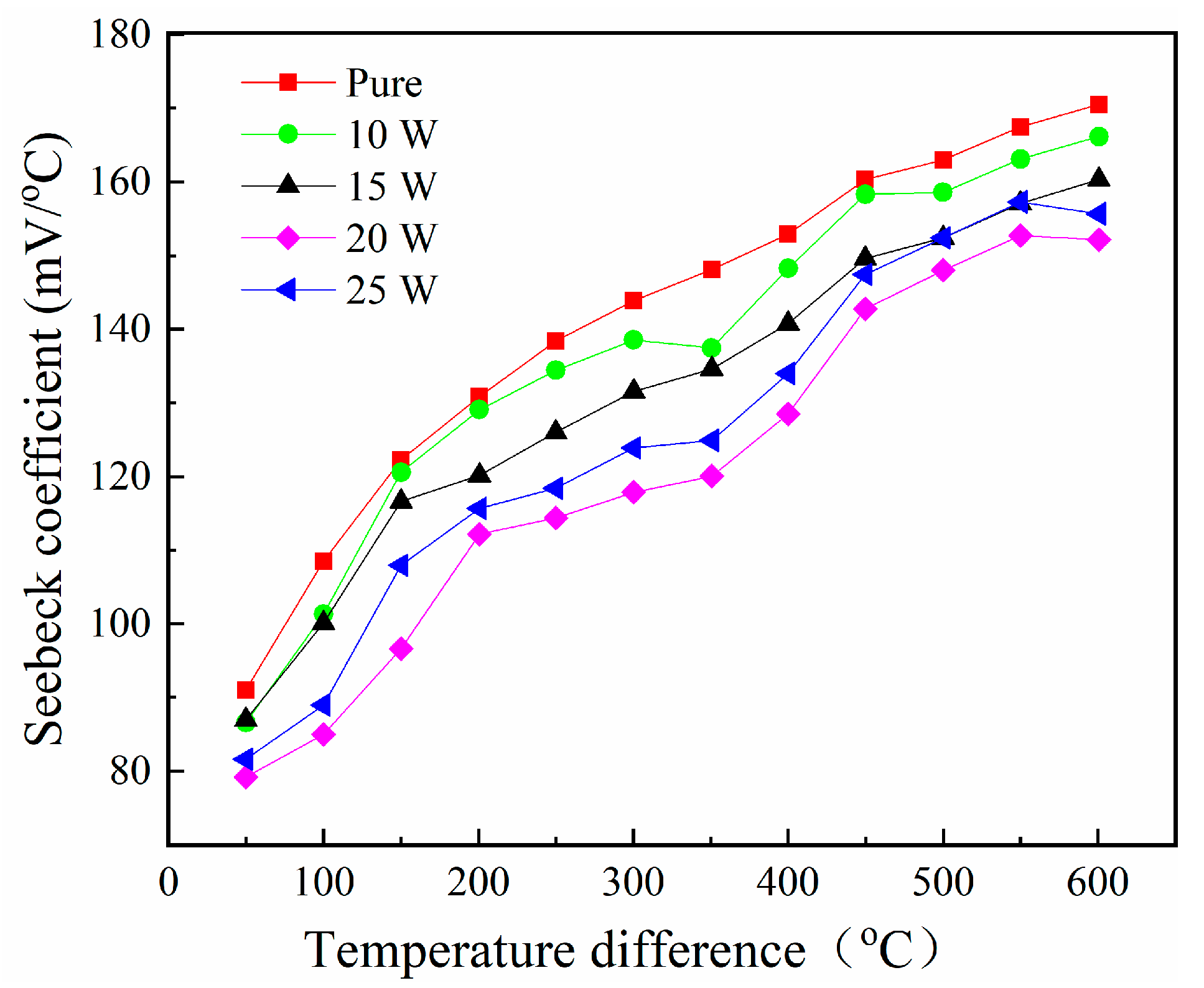
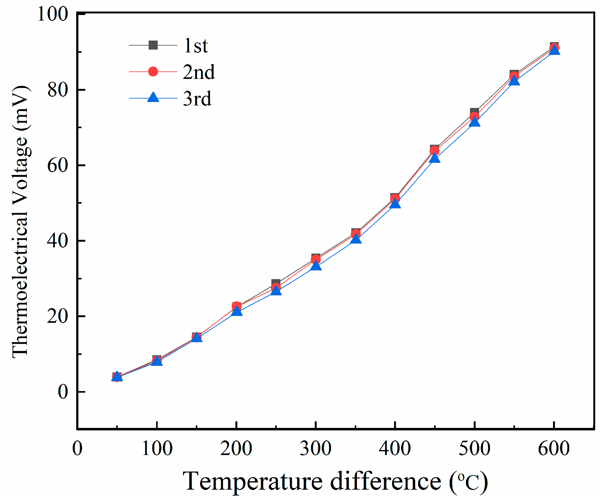
3.4. Thermoelectrical Properties of Cu-Doped In2O3 Thin Films

To measure the output characteristics of the In2O3/Pt thermocouple, all electrodes were connected using enameled copper wire with a diameter of 0.2 mm and a length of 10 cm. The wire was bonded with silver paste; the contact was between the wire and the two electrodes. Figure 15 presents the thermoelectrical output voltage of the Cu-doped In2O3 films under different DC powers from room temperature to 600 °C. The output value was 102.4 mV at 0 DC power and a temperature difference of 600 °C. The absolute value of the output thermal voltage of the sample under 20 W DC power was 91.4 mV. The Seebeck coefficients of the Cu-doped In2O3 thin films were tested as a function of the hot-end temperature. The Seebeck coefficient was obtained using Equation (4) [44]:
S = Δ V Δ T = ( Δ V a Δ V b T h T c )
where S is the Seebeck coefficient, ∆V is the voltage difference between the two different electrode materials, and ∆T is the temperature difference between the hot end (Th) and the cold end (Tc). As In2O3 is an n-type semiconductor, its output is negative; thus, the absolute value of the Seebeck coefficient of the Pt electrode was much smaller than that of the indium oxide material [45]. Figure 16 presents the trends of the Seebeck coefficient with the temperature variation. The Seebeck coefficient of the Cu-doped In2O3 films increased with an increase in the temperature difference. When the temperature difference between the two ends of the thin film samples reached 600 °C, the Seebeck coefficient increased to 170.5 μV/°C under 0 DC power. The Seebeck coefficient of Cu-doped In2O3 thin films under 20 W DC power reached 152.1 μV/°C; it reached 155.6 μV/°C under 25 W DC power. The Seebeck coefficient of the In2O3 thin films could be expressed by Equation (5) [44]:
S ( N D ) = A k e k e ( ( 2 π m c * k T ) 2 3 h 3 N D )
where S is the Seebeck coefficient, k is the Boltzmann constant, e is the electron charge, mc is the effective mass, h is the Planck constant, and A is the transport constant. The carrier concentration of the doped In2O3 thin films clearly changed due to different doping levels. This was observed from the electrical performance results of the Cu-doped In2O3 thin films. Under a DC power of 20 W, the carrier concentration reached its maximum value, resulting in the smallest overall Seebeck coefficient of the corresponding sample. The carrier concentration was the main factor affecting the variations in the Seebeck coefficients in the temperature range from room temperature to 600 °C. Figure 17 presents the output voltage of the Cu-doped In2O3 films under 20 W DC power for three heating processes. In the third heating process, the output value reached 89.3 mV at a 600 °C temperature difference; the Seebeck coefficient reached 148.8 μV/°C. The measurement results of the three heating processes indicated that the thermocouple had good repeatability.

4. Conclusions

In summary, this paper presents the preparation as well as the morphological, electrical, and optical properties of pure and Cu-doped In2O3 thin films fabricated using the magnetron co-sputtering process. The doping of copper effectively adjusted the optoelectronic properties of the In2O3 thin films and significantly impacted the output performance of the thermocouple. When the Cu atomic content increased to 4.09% (under 20 W DC sputtering power), the Cu-doped thin films possessed the highest resistivity (30.2 × 10⁻³ Ω·cm) and carrier concentration (3.72 × 10⁻¹⁹ cm−3) as well as the lowest carrier mobility (0.56 cm2V−1s−1). Copper doping resulted in a significant reduction in the optical band gap. Consequently, the band gap of Cu-doped In2O3 was narrower than that of undoped In2O3. The optical band gap was reduced to 2.71 eV when the DC power was 20 W. The Seebeck coefficient of the undoped In2O3/Pt thermocouple reached a maximum of 170.5 μV/°C and an output value of 106.5 mV at a high-temperature range of 600 °C. When the DC sputtering power was 20 W, the output value of the sample was 91.4 mV and the Seebeck coefficient was 152.1 μV/°C.

Author Contributions

Formal analysis, Y.L., T.L., R.H., J.S. and S.C.; investigation, Y.L., T.L. and R.H.; writing, Y.L. and R.H.; writing—review and editing, Y.L., T.L., R.H., J.S. and S.C.; supervision, Y.L., T.L. and R.H. All authors have read and agreed to the published version of the manuscript.

Funding

This research was supported by the Shaanxi Provincial Department of Education Youth Innovation Team Project (No. 22JP051).

Data Availability Statement

Data are contained within the article.

Conflicts of Interest

The authors declare no conflicts of interest.

References

  1. Sakthivel, P.; Murugana, R.; Asaithambi, S.; Karuppaiah, M.; Vijayaprasath, G.; Rajendran, S.; Hayakawa, Y.; Ravi, G. Studies on optoelectronic properties of magnetron Sputtered cadmium stannate (Cd2SnO4) thin films as alternative TCO materials for solar cell applications. Ceram. Int. 2018, 44, 2529–2538. [Google Scholar] [CrossRef]
  2. Sakthivel, P.; Murugan, R.; Asaithambi, S. Influence of radiofrequency power on structural, morphological, optical and electrical properties of magnetron sputtered CdO: Sm thin films as alternative TCO for optoelectronic applications. J. Alloys Compd. 2018, 765, 146–157. [Google Scholar] [CrossRef]
  3. Chan, Y.P.; Seong, P.J.; Joon, B.P. High-performance ITO/a-IGZO heterostructure TFTs enabled by thickness-dependent carrier concentration and band alignment manipulation. Ceram. Int. 2023, 49, 5905–5914. [Google Scholar]
  4. Sarath, R.; Narasimha, M.Y.; Hari, P.K.; Alshahrani, T.; Sarah, J.M.; Mohd, S.; AlFaify, S. Enhancement in optoelectronic nature of facile spray fabricated Ce co-doped CdO:Zn films for TCO applications. Optik 2020, 223, 165408. [Google Scholar]
  5. Husam, R.A.; Ameer, I.K.; Ali, A.Y. AImpact of high vacuum annealing temperature on the structural, photoluminescence, and room temperature liquefied petroleum gas sensing of direct current magnetron sputtered CdO films. Mater. Chem. Phys. 2022, 289, 126446. [Google Scholar]
  6. Liu, Y.T.; Wang, W.X.; Ma, J.P. Structure, optical and electrical properties of Nb-doped ZnO transparent conductive thin films prepared by co-sputtering method. J. Adv. Dielect. 2019, 9, 1950048. [Google Scholar] [CrossRef]
  7. Daseul, H.; Seongchan, O.; Hyon, C.K. Competing phases in epitaxial SnO2 thin films deposited on sapphire (0001) substrates using radio-frequency powder sputtering. Ceram. Int. 2022, 48, 28396–28403. [Google Scholar]
  8. Afroz, K.; Rahman, F.; Razia, N.; Asokan, K. Role of deposition temperature and Sn content on structural, optical & electrical properties of In2O3 thin films. Curr. Appl. Phys. 2022, 38, 49–58. [Google Scholar]
  9. Vilca-Huayhua, C.A.; Paz-Corrales, K.J.; Aragón, F.F.H.; Mathpalb, M.C.; Villegas, L.L.; Coaquira, J.A.H.; Pacheco-Salazara, D.G. Growth and vacuum post-annealing effect on the structural, electrical and optical properties of Sn-doped In2O3 thin films. Thin Solid Film. 2020, 709, 138207. [Google Scholar] [CrossRef]
  10. Ehsan, E.; Fariborz, T. Development of highly sensitive ZnO/In2O3 composite gas sensor activated by UV-LED. Sens. Actuators B 2017, 241, 828–839. [Google Scholar]
  11. Nasrin, J.; Mohsen, G.; Vishtasb, S. Investigation of the role of deposition rate on optical, microstructure and ethanol sensing characteristics of nanostructured Sn doped In2O3 films. MRS Bull. 2018, 106, 49–56. [Google Scholar]
  12. Rombach, J.; Bierwagen, O.; Papadogianni, A.; Mischob, M.; Cimalla, V.; Berthold, T.; Krischok, S.; Himmerlich, M. Electrical conductivity and gas-sensing properties of Mg-doped and undoped single-crystalline In2O3 thin films: Bulk vs. Surface. Procedia Eng. 2015, 120, 79–82. [Google Scholar] [CrossRef]
  13. Pramodn, N.; Pandey, S. Effect of Li doping on the structural, optical and formaldehyde sensing properties of In2O3 thin films. Ceram. Int. 2015, 41, 527–532. [Google Scholar] [CrossRef]
  14. Shinozaki, B.; Takada, S.; Kokubo, N. Superconducting characteristics and microstructure of polycrystalline Zn-doped In2O3 films. Physica C 2011, 471, 717–720. [Google Scholar] [CrossRef]
  15. Pramodn, N.; Pandey, S. Influence of Sb doping on the structural, optical, electrical and acetonesensing properties of In2O3 thin films. Ceram. Int. 2014, 40, 3461–3468. [Google Scholar] [CrossRef]
  16. Moustafa, A.; Ahmed, B.; Essam, R.S. Optical characteristics with high accuracy of diluted Cr doped In2O3 thin films using spectroscopic ellipsometry for optoelectronic devices. Opt. Mater. 2022, 133, 113039. [Google Scholar]
  17. Jianhua, S.; Fanying, M.; Jian, B.; Yongwu, L.; Zhengxin, L. Surface scattering effect on the electrical mobility of ultrathin Ce doped In2O3 film prepared at low temperature. Mater. Lett. 2018, 225, 54–56. [Google Scholar]
  18. Wang, G.H.; Shi, C.Y.; Zhao, L. Efficiency improvement of the heterojunction solar cell using an antireflection Hf-doped In2O3 thin film prepared via glancing angle magnetron sputtering technology. Opt. Mater. 2020, 109, 110323. [Google Scholar] [CrossRef]
  19. Chaeyoung, K.; Hae, J.S.; Seong, W.K. Ga and Ti co-doped In2O3 films for flexible amorphous transparent conducting oxides. Ceram. Int. 2022, 48, 13938–13947. [Google Scholar]
  20. Kaleemulla, S.; Rao, N.M. Electrical and optical properties of In2O3:Mo thin films prepared at various Mo-doping levels. J. Alloys Compd. 2010, 504, 351–356. [Google Scholar] [CrossRef]
  21. Fan, Y.; Xing, M.C.; Xue, Z.; Tian, X.Q. The electrical and optical properties of Cu-doped In2O3 thin films. Thin Solid Film. 2014, 556, 44–47. [Google Scholar]
  22. Gregory, O.J.; Tougas, I.M.; Amani, M.; Crisman, E.E. Thermoelectric Properties and Microstructure of Cu-In-O Thin Films. ACS Comb. Sci. 2013, 15, 580–584. [Google Scholar] [CrossRef] [PubMed]
  23. Gupta, R.K.; Ghosh, K.; Mishra, S.R.; Kahol, P.K. High mobility, transparent, conducting Gd-doped In2O3 thin films by pulsed laser deposition. Thin Solid Film. 2008, 516, 3204–3209. [Google Scholar] [CrossRef]
  24. Salvador, A.; Palomares, S.; Bernard, E. Sol-gel growth and characterization of In2O3 thin films. Thin Solid Film. 2018, 645, 383–390. [Google Scholar]
  25. Baqiah, H.; Ibrahim, N.B. Electrical transport, microstructure and optical properties of Cr-doped In2O3 thin film prepared by sol-gel method. J. Alloys Compd. 2013, 575, 198–206. [Google Scholar] [CrossRef]
  26. Xuejian, D.; Jing, Y.; Xianwu, X.; Qianqian, S.; Wei, T.; Baoyuan, M. Epitaxial growth and characterization of high quality In2O3 films on a-plane sapphire substrates by MOCVD. Vacuum 2019, 167, 1–5. [Google Scholar]
  27. Shinho, C. Effects of rapid thermal annealing on the properties of In2O3 thin films grown on glass substrate by rf reactive magnetron sputtering. Microelectron. Eng. 2012, 89, 84–88. [Google Scholar]
  28. Zijian, Y.; Xiaming, Z.; Xiong, W.; Xikun, C.; Bingpo, Z.; Dongjiang, Q.; Huizhen, W. Annealing effects of In2O3 thin films on electrical properties and application in thin film transistors. Thin Solid Film. 2011, 519, 3254–3258. [Google Scholar]
  29. Otto, J.G.; Qing, L.; Everett, E.C. High temperature stability of indium tin oxide thin films. Thin Solid Film. 2002, 406, 286–293. [Google Scholar]
  30. Dyer, S.E.; Gregory, O.J.; Amons, P.S.; Slot, B.A. Preparation and piezoresistive properties of reactively sputtered indium tin oxide thin films. Thin Solid Film. 1996, 288, 279–286. [Google Scholar] [CrossRef]
  31. Zhao, X.H.; Li, H.T.; Jiang, S.W.; Zhang, W.L.; Jiang, H.C. Effect of nitrogen doping on the thermoelectric properties of ITO-In2O3 thin film thermocouples. Thin Solid Film. 2017, 629, 1–5. [Google Scholar] [CrossRef]
  32. Liu, D.; Shi, P.; Ren, W. Fabrication and characterization of La0.8Sr0.2CrO3/In2O3 thin film thermocouple for high temperature sensing. Sens. Actuators A 2018, 280, 459–465. [Google Scholar] [CrossRef]
  33. Zhao, X.H.; Li, H.T.; Chen, Y.Z.; Jiang, H.C. Preparation and thermoelectric characteristics of ITO/Pt thin film thermocouples on Ni-based superalloy substrate. Vacuum 2017, 140, 116–120. [Google Scholar] [CrossRef]
  34. Zhang, Z.K.; Tian, B.; Li, L.; Lei, J.M.; Liu, Z.J.; Liu, J.J.; Cheng, G.; Zhao, N.; Fang, X.B.; Zhao, L.B. The electrical and optical properties of Cu-doped In2O3 thin films. Ceram. Int. 2022, 48, 25747–25755. [Google Scholar] [CrossRef]
  35. Zhao, X.H.; Li, H.T.; Yang, K.; Jiang, S.W.; Jiang, H.C.; Zhang, W.L. Annealing effects in ITO based ceramic thin film thermocouples. J. Alloys Compd. 2017, 698, 147–151. [Google Scholar] [CrossRef]
  36. Liu, Y.T.; Ren, W.; Shi, P.; Liu, D. Preparation and thermal volatility characteristics of In2O3/ITO thin film thermocouple by RF magnetron sputtering. AIP Adv. 2017, 7, 1150251–1150258. [Google Scholar] [CrossRef]
  37. Jingli, S.; Feng, L.; Bo, Y.; Liang, S.; Chuan, C.; Shanpeng, W.; Yu, C.; Shengping, R. Enhanced ethyl acetate sensing performance of Al-doped In2O3 microcubes. Sens. Actuators B 2017, 253, 461–469. [Google Scholar]
  38. Asma, A.; Azra, P. Tuning the structural, optical, and magnetic properties of In2O3 nanoparticles with an evaluation of its antibacterial efficiency via controlling the doping concentrations of Ni, Co, and Fe. Mater. Today Commun. 2022, 30, 103063. [Google Scholar]
  39. Shanmuga, P.B.; Shanthi, M.; Manoharan, C.; Bououdina, M. Hydrothermal synthesis of Ga-doped In2O3 nanostructure and its structural, optical and photocatalytic properties. Mater. Sci. Semicond. Process. 2017, 71, 357–365. [Google Scholar] [CrossRef]
  40. Mengting, L.; Qiuqiang, Z.; Wei, L.; Rui, L.; Qinyu, H.; Yinzhen, W. Effect of Zn doping concentration on optical band gap of PbS thin films. J. Alloys Compd. 2019, 792, 1000–1007. [Google Scholar]
  41. Miao, W.; Li, X.; Zhang, Q. Transparent conductive In2O3:Mo thin films prepared by reactive direct current magnetron sputtering at room temperature. Thin Solid Film. 2006, 500, 70–73. [Google Scholar] [CrossRef]
  42. Fernando, P.S.; Su, H.W.; Anderson, J. Enabling visible-light absorption and p-type doping in In2O3 by adding Bi. Phys. Rev. Mater. 2019, 3, 034605. [Google Scholar]
  43. Nasser, Y.M.; Ali, B.; Sameh, I.A. Influence of Cu and Ag doping on structure and optical properties of In2O3 thin film prepared by spray pyrolysis. Results Phys. 2018, 10, 126–131. [Google Scholar]
  44. Ian, M.T.; Matin, A.; Otto, J.G. Metallic and Ceramic Thin Film Thermocouples for Gas Turbine Engines. Sensors 2013, 13, 15324–15347. [Google Scholar]
  45. Liu, Y.T.; Ren, W.; Shi, P.; Liu, D. Highly Thermostable In2O3/ITO Thin Film Thermocouple Prepared via Screen Printing for High Temperature Measurements. Sensors 2018, 18, 958. [Google Scholar] [CrossRef]
Figure 1. Schematic diagram of magnetron co-sputtering.
Crystals 14 00078 g001
Figure 2. Physical image of a test sample of an In2O3/Pt thermocouple.
Crystals 14 00078 g002
Figure 3. The process diagram of the In2O3/Pt thermocouple preparation.
Crystals 14 00078 g003
Figure 4. Schematic diagram of the thermal voltage testing system.
Crystals 14 00078 g004
Figure 5. (a) XRD patterns of Cu-doped thin film samples; (b) diffraction peaks (622).
Crystals 14 00078 g005
Figure 6. Crystallite size of Cu-doped In2O3 thin films.
Crystals 14 00078 g006
Figure 7. Morphology of Cu-doped In2O3 thin films under different DC powers: (a) pure and unannealed; (b) 0 W; (c) 15 W; (d) 25 W. (e) Cross-section image under 0 W DC power.
Crystals 14 00078 g007
Figure 8. AFM images of the surface topography of Cu-doped In2O3 thin films under different DC powers: (a) 0 W; (b) 10 W; (c) 15 W; (d) 20 W; (e) 25 W.
Crystals 14 00078 g008
Figure 9. Surface roughness of Cu-doped In2O3 thin films under different DC powers.
Crystals 14 00078 g009
Figure 10. EDX patterns of Cu-doped In2O3 thin films under different DC powers.
Crystals 14 00078 g010
Figure 11. Cu content of doped In2O3 thin films under different DC powers.
Crystals 14 00078 g011
Figure 12. Variations in the resistivity, carrier concentration, and mobility of the films under DC sputtering powers.
Crystals 14 00078 g012
Figure 13. Transmittance spectra of In2O3 thin films.
Crystals 14 00078 g013
Figure 14. (αhv)2 vs. hv of In2O3 thin films.
Crystals 14 00078 g014
Figure 15. Thermoelectrical output voltage of Cu-doped In2O3/Pt thermocouple under different DC powers.
Crystals 14 00078 g015
Figure 16. Variations in the Seebeck coefficients of a Cu-doped In2O3/Pt thermocouple under different DC powers.
Crystals 14 00078 g016
Figure 17. Variations in the In2O3/Pt thermocouple output voltage for three heating processes under 20 W DC power.
Crystals 14 00078 g017
Table 1. Parameters of indium oxide and copper targets during co-sputtering.
TargetSputtering MethodSputtering Power (W)Sputtering Time (h)Argon Gas Flow Rate (sccm)Oxygen Flow Rate (sccm)
In2O3RF10036010
CuDC0–253
Disclaimer/Publisher’s Note: The statements, opinions and data contained in all publications are solely those of the individual author(s) and contributor(s) and not of MDPI and/or the editor(s). MDPI and/or the editor(s) disclaim responsibility for any injury to people or property resulting from any ideas, methods, instructions or products referred to in the content.

