Review

Raman Spectroscopy of 2D MoS2 Interacting with Metals

1
Department of Physics, Engineering Physics and Astronomy, Queen’s University, 64 Bader Lane, Kingston, ON K7L 3N6, Canada
2
Department of Energy, Politecnico di Milano, Via Ponzio 34/3, 20133 Milano, Italy
*
Author to whom correspondence should be addressed.
Crystals 2023, 13(8), 1271; https://doi.org/10.3390/cryst13081271
Submission received: 17 July 2023 / Revised: 8 August 2023 / Accepted: 15 August 2023 / Published: 17 August 2023
(This article belongs to the Special Issue Raman Spectroscopy of Crystalline Materials and Nanostructures)

Abstract

:
The research on molybdenum disulphide (MoS 2 ) has progressed remarkably in the last decade, prompted by the increasing interest for this material as a potential candidate in future ultrathin optoelectronic devices. MoS 2 is a layered semiconductor with a gap in the visible region, which can be exfoliated down to the mono-layer form. Since the discovery of the exceptional optoelectronic properties of 2D MoS 2 , Raman spectroscopy has been extensively used as a tool to characterize the structure and thickness of MoS 2 films. Recent works on MoS 2 -metal interfaces have shown that Raman spectra are significantly affected by the interaction with metals. However, a complete understanding of how such interaction modifies the MoS 2 vibrational properties is still lacking. Studying this subject with both experimental and theoretical methods will provide fundamental insight into the interface physics of MoS 2 -metal systems, which is crucial for the fabrication of metal contacts and for the development of metal-assisted synthesis methods. This review summarizes the main results concerning Raman spectroscopy studies of heterosystems between MoS 2 and transition metals, providing both a basis and directions for future research.

1. Introduction

Transition metal dichalcogenides (TMDs) are a technologically relevant class of layered materials that have attracted increasing interest due to their intriguing optical and electronic properties [1,2,3,4,5,6,7,8,9,10]. The most prominent member of the TMD class is molybdenum disulphide (MoS 2 ), which has a longstanding tradition of industrial applications as a solid lubricant and catalyst for desulfurization reactions. Following the isolation of graphene and the discovery of its exceptional properties, the interest in layered materials such as MoS 2 and other TMDs shifted on the study of 2D systems formed by one or few-layers, obtained by exfoliation of a bulk crystal. This study led to the remarkable discovery of the gap variation and indirect-to-direct gap transition occurring in MoS 2 and other TMDs as the number of layers is reduced down to a single one [11]. The observation of this bandstructure evolution boosted the research on MoS 2 as a promising candidate for 2D optoelectronic devices, prompted also by its high carrier mobility at room temperature [12].
The future application of MoS 2 in real devices requires one to face several challenges, such synthesizing large-area films of high crystalline quality, assessing their stability under operating conditions, and obtaining a detailed understanding of the interface properties of MoS 2 -metal heterosystems. The latter is necessary to design and engineer functional metal contacts in electronic devices. Moreover, the deposition of MoS 2 on metal surfaces—either by exfoliation or bottom-up growth—has been recently explored as a promising method to obtain mono-layer MoS 2 films of a relatively large-area [13,14,15,16,17,18]. The interaction with metals is known to have profound effects on the electronic properties of mono-layer MoS 2 [19,20], due to the hybridization with metal states causing, e.g., band gap renormalization and partial metallization [20,21]. Less is known about the impact of a metal interface on the vibrational properties of 2D MoS 2 , and about how they are affected by metal-induced effects, such as interface strain and charge transfer.
Raman spectroscopy has been proved to be one the most valuable techniques to characterize the lattice vibrations of 2D MoS 2 and obtain information on its structure as well as the influence of additional factors, such as strain, doping, and defects [22,23,24,25,26,27,28,29,30,31,32,33,34]. Notably, Raman spectroscopy is highly sensitive to the number of atomic layers [23,24], providing a widely used method to measure the thickness of MoS 2 films. This is the main reason why Raman spectroscopy is extensively used to characterize exfoliated or chemical-vapor-deposited (CVD) MoS 2 , which is typically supported by SiO 2 /Si substrates. Since MoS 2 interacts weakly with such substrates, it can be considered as quasi-freestanding, and its properties are unperturbed by the support. However, when MoS 2 interacts with metals, Raman spectra show significant deviations from the vibrational features of quasi-freestanding MoS 2 [16,35,36,37,38,39,40,41,42,43], suggesting a strong sensitivity of MoS 2 Raman active modes to metal-induced interface effects, such as strain and charge transfer. Similarly to other MoS 2 heterostructures [44], Raman spectra of MoS 2 -metal systems can therefore be used as a fingerprint of the interaction strength and other interface effects, providing a valuable insight into the interface physics of these systems.
In the last decade, MoS 2 and its heterostructures have been studied using a wide range of fabrication approaches and characterization techniques. Consequently, the related literature has grown enormously, and many reviews focusing on different aspects of this research field have been published in recent years [1,2,3,4,5,6,7,8,9,10]. We refer the reader to such works for a more comprehensive overview of the fabrication and characterization techniques that have been applied to the study of MoS 2 and its heterostructures. The scope of this review is to focus on recent Raman spectroscopy studies of MoS 2 -metal heterosystems. The interest in these systems embraces many potential applications and categories of metals, including, e.g., MXenes [45,46] or conductive polymers [47]. In particular, we will focus on the Raman spectroscopy studies of MoS 2 heterostructures with transition metals, which are interesting systems for electronic devices and metal-assisted MoS 2 synthesis. The discussion of these studies is presented in Section 3. Before that, Section 2 provides a short summary of the vibrational properties of quasi-freestanding MoS 2 , which are useful to the discussion of MoS 2 -metal systems.

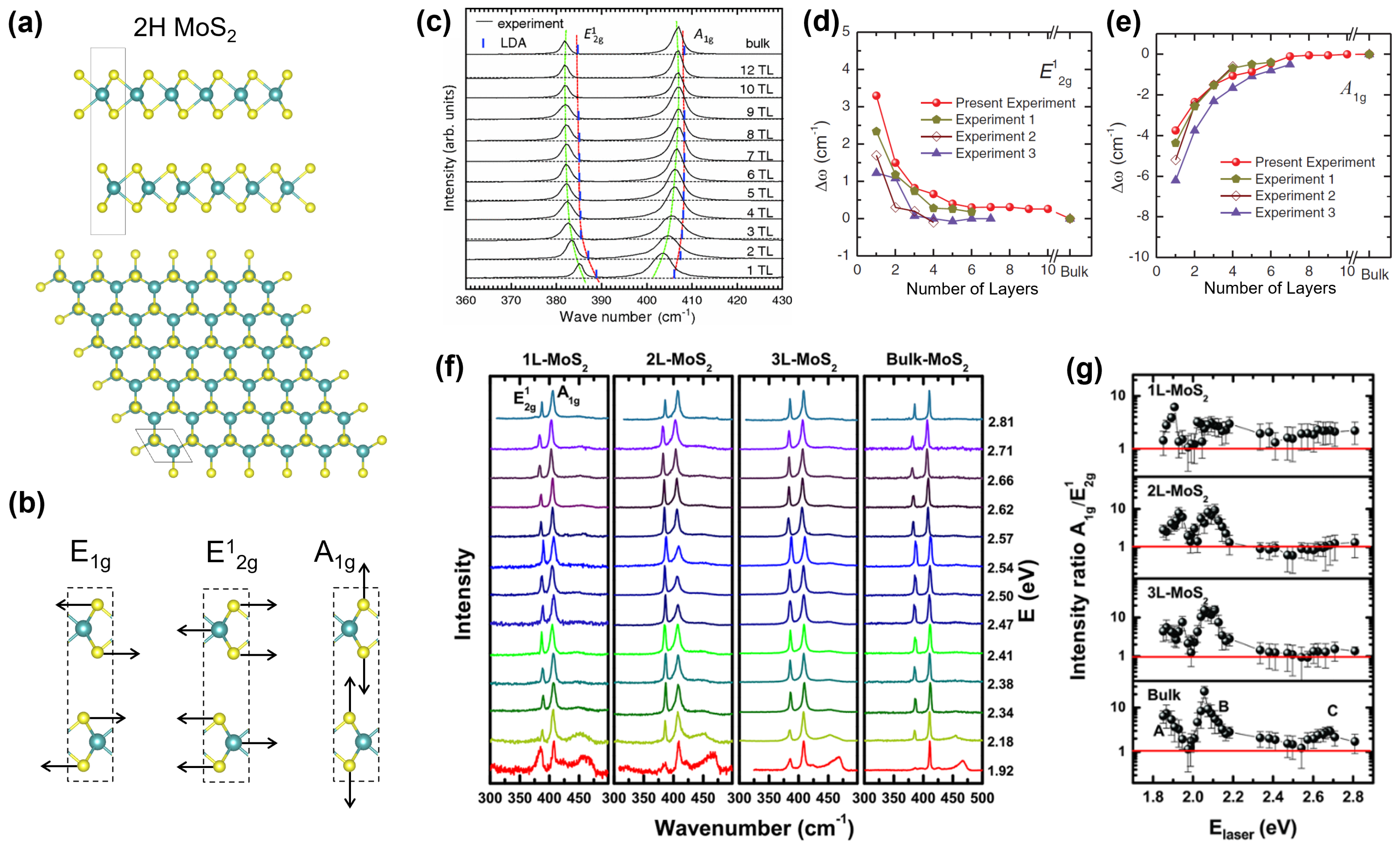
2. Lattice Vibrations of Quasi-Freestanding MoS2

Bulk MoS 2 is a layered semiconducting material composed by weakly bound layers that can be easily exfoliated, e.g., using common adhesive tape. The mono-layer is composed of a plane of Mo atoms covalently bound to two planes of S atoms. The most stable bulk phase is the 2H polytype, whose structure is shown in Figure 1a. Its unit cell consists of two Mo and four S atoms, and the crystal has D 6 h symmetry. The mono-layer has D 3 h symmetry, and its unit cell contains only one Mo and two S atoms. According to the irreducible representation of D 3 h , the optical Raman active modes of the mono-layer correspond to E , E , and A 1 symmetries [48]. The geometries of these modes, respectively, correspond to the Raman active E 2 g 1 , E 1 g , and A 1 g modes in the bulk. Albeit the notation of vibrational modes varies among mono-layer, bi-layer, and bulk (precisely, the symmetry changes from D 3 h in odd-layers MoS 2 to D 3 d in even-layers MoS 2 ), the use of the bulk notation to also label the vibrational modes of few-layers MoS 2 is quite common in the literature. In this review, we use the same notation used in the papers that we will discuss, partly to avoid conflicts with the original figure labeling.
Figure 1b reports the vibration geometries of the E 1 g , E 2 g 1 , and A 1 g modes. E 1 g and E 2 g 1 correspond to in-plane vibrations and are doubly degenerate at the zone center, whereas A 1 g is an out-of-plane vibration of S atoms. In both bulk and mono-layer MoS 2 , the E 1 g ( E ) mode (at ∼280 cm 1 ) requires a scattering geometry involving an out-of-plane component of the field [22,26]. Therefore, it is usually not detected in backscattering configuration, where the laser polarization is parallel to the MoS 2 basal plane. Typical Raman spectra of mono-layer MoS 2 show the E mode at ∼384 cm 1 and the A 1 mode at ∼403 cm 1 . The frequency of the two modes notably depends on the number of MoS 2 layers (Figure 1c). As the number of layers increases, E 2 g 1 gradually downshifts while A 1 g upshifts (Figure 1d,e). For a number of layers larger than six, the frequencies of both modes converge to the bulk values, namely, 382 cm 1 for E 2 g 1 and 408 cm 1 for A 1 g . Due to this opposite shift, the frequency difference between the two modes in the mono-layer is 19 cm 1 , and it gradually increases to 26 cm 1 in the bulk. Therefore, this parameter can be used to infer the thickness of an MoS 2 film [23,24,25].
The intensity of Raman modes depends on the excitation wavelength, and resonance scattering can also enhance second-order processes. The latter effect is particularly evident when the excitation energy is close to the energy of the A exciton (1.88 eV at room temperature). The result is the resonant Raman spectrum of MoS 2 , which has been extensively analyzed in previous works [50,51,52]. Carvalho et al. [49] have measured the Raman spectra of mono-, bi-, tri-layer, and bulk MoS 2 using more than 30 different laser excitation lines covering the visible range (1.85–2.81 eV) (Figure 1f). They analyzed the intensity of E 2 g 1 and A 1 g modes as a function of the excitation energy and found out that the excitonic A, B, and C transitions enhance the intensity of both modes. The intensity ratio A 1 g / E 2 g 1 plotted in Figure 1g also shows that A 1 g is typically more intense than E 2 g 1 , being the ratio larger than 1 for almost all excitation energies in the investigated spectral range.
The behavior of MoS 2 vibrational modes is also affected by other perturbations, such as strain, doping, and defects. We will briefly review the effects of these three main factors as they can also be relevant in the following discussion of metal-MoS 2 heterosystems.
Strain has important consequences on the electronic bandstructure, phonon dispersion, and charge transport properties. Several works have shown the possibility of sensibly tuning the MoS 2 band gap by applying moderate uniaxial or biaxal in-plane strain [27,28,29,30,31]. The effect of in-plane strain on the vibrational properties depends on whether the strain is uniaxial or biaxial. Unixial strain breaks the symmetry of the crystal lattice in the basal plane and lifts the degeneracy of E at Γ . This effect can be observed in Raman spectra as a splitting of the E mode for increasing strain. Conley et al. [27] measured such splitting as a function of tensile strain between 0 and 2% (Figure 2a,b) and found that while E is strongly sensitive to in-plane uniaxial strain, A 1 is essentially unperturbed. Biaxial strain, on the other hand, does not produce anisotropy in the crystal lattice. Therefore, the degeneracy of E is not lifted. Both modes upshift (downshift) as compressive (tensile) biaxial strain is applied. Lloyd et al. [29] studied the effect of tensile biaxial strain by applying a pressure difference to MoS 2 layers suspended over cylindrical microcavities (Figure 2c). They reported a softening of both modes that is more pronounced in mono-layer MoS 2 (Figure 2d). The Raman modes downshift linearly at a rate of 1.7 cm 1 /% for A 1 g and 5.2 cm 1 /% for E 2 g 1 . Interestingly, they also observed that as biaxial strain increases, the A 1 g / E 2 g 1 intensity ratio significantly decreases below 1, as also supported by theoretical calculations [32].
Doping generally has a strong impact on the vibrational properties of a crystal as changes in the electron concentration modify the electron-phonon coupling. Chakraborty et al. [33] studied the correlation between doping and the behavior of Raman modes in mono-layer MoS 2 . They used a top-gated mono-layer MoS 2 transistor to modulate the electron concentration up to 2 × 10 13 cm 2 (Figure 2e). Raman spectra taken at different gate voltages show that A 1 strongly depends on the doping level, whereas E is much less sensitive. For the maximum electron concentration, the A 1 frequency softens by 4 cm 1 and the linewidth broadens by 6 cm 1 . The E mode downshifts by only 0.6 cm 1 , and its linewidth is not appreciably affected. This result is explained in terms of a stronger electron-phonon coupling of the A 1 mode compared to E , confirmed with first-principles DFT calculations and symmetry arguments.
Variations in the frequency and shape of Raman peaks can be also due to lattice defects. In general, due to translation symmetry, a crystalline material satisfies the Raman fundamental selection rule q 0 ( q is the phonon wavevector), leaving only the zone center phonons as Raman active. In contrast, due to the loss of long-range order, the q -selection rule is relaxed in a defective lattice, thus allowing other features related to the phonon dispersion away from the zone center to be detected in Raman spectra. Mignuzzi et al. [34] studied the Raman response of defective mono-layer MoS 2 flakes, exfoliated from the bulk on SiO 2 and then bombarded with different densities of Mn + ions. The degree of disorder is quantified by the average interdefect distance L D , which can be derived from the ion density. Figure 2g reports the Raman spectra obtained for different values of the L D parameter. As disorder increases (i.e., decreasing L D ), E and A 1 change in both their widths and frequencies. The increasing defect density produces a downward shift of the E mode and an upward shift of A 1 . This opposite trend is due to the phonon dispersion of the corresponding branches (Figure 2h): moving away from Γ , the frequency of the ZO branch increases, while that of the LO and TO branches decreases. The asymmetric broadening of the two main Raman modes can be ascribed to the activation of the ZO, TO, and LO phonons at the M point of the Brillouin zone.

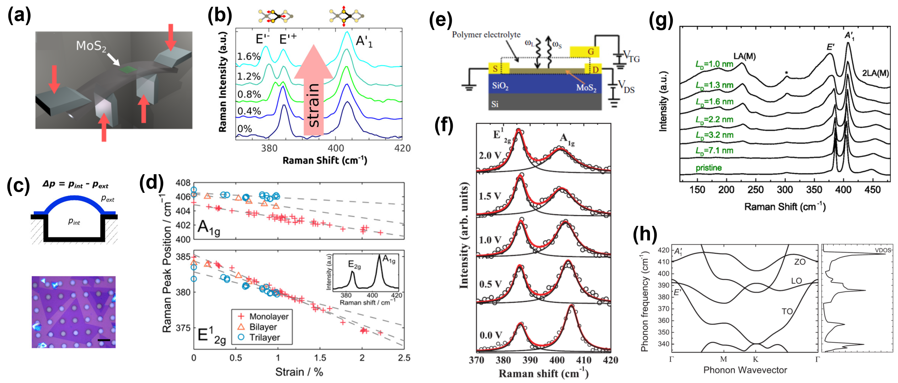
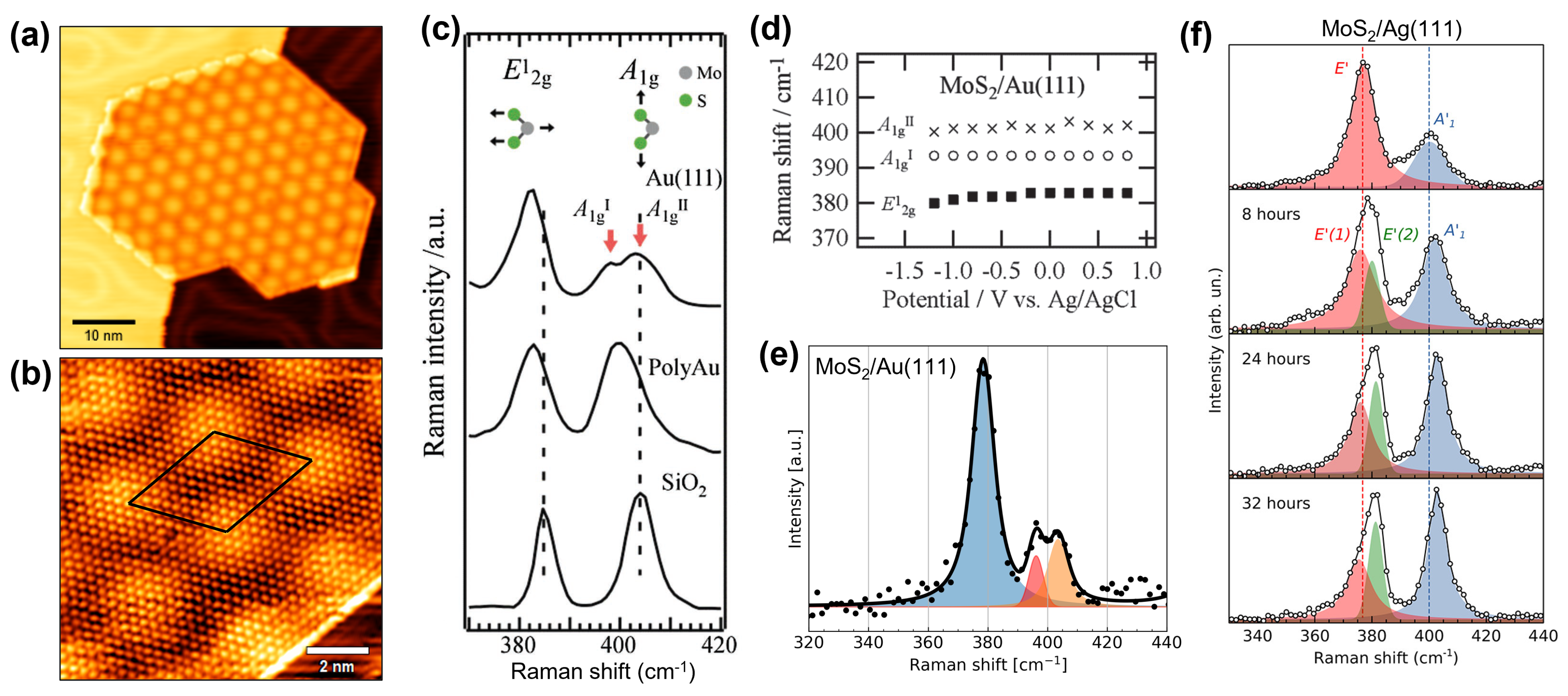
3. Vibrational Properties of Metal-MoS2 Heterosystems

The interface properties of MoS 2 -metal junctions are of key importance for the performances of MoS 2 -based devices [53,54,55]. The charge transport at the MoS 2 -metal interface is strongly dependent on the interaction between the two materials and metal-induced modifications to MoS 2 electronic structure, e.g., due to Fermi level pinning and hybridization with metal states [19,20,21,56]. Strain and charge transfer induced by the contact with metals are additional interface phenomena that can perturb the MoS 2 properties. As discussed in the previous section, Raman spectroscopy is sensitive to strain and doping effects and can therefore provide valuable insight into the interface properties of metal-MoS 2 heterosystems.
Different fabrication approaches have been used for the experimental investigation of such systems. We can divide them in three categories:
  • The deposition of a metal film on the MoS 2 surface.
  • The exfoliation of a bulk MoS 2 crystal on metals.
  • The direct growth of MoS 2 layers on a metal surface.
These approaches produce metal-MoS 2 systems with different interface morphologies, therefore giving different results concerning the study of the vibrational properties. We will review the three fabrication approaches and the corresponding Raman studies in the following subsections.

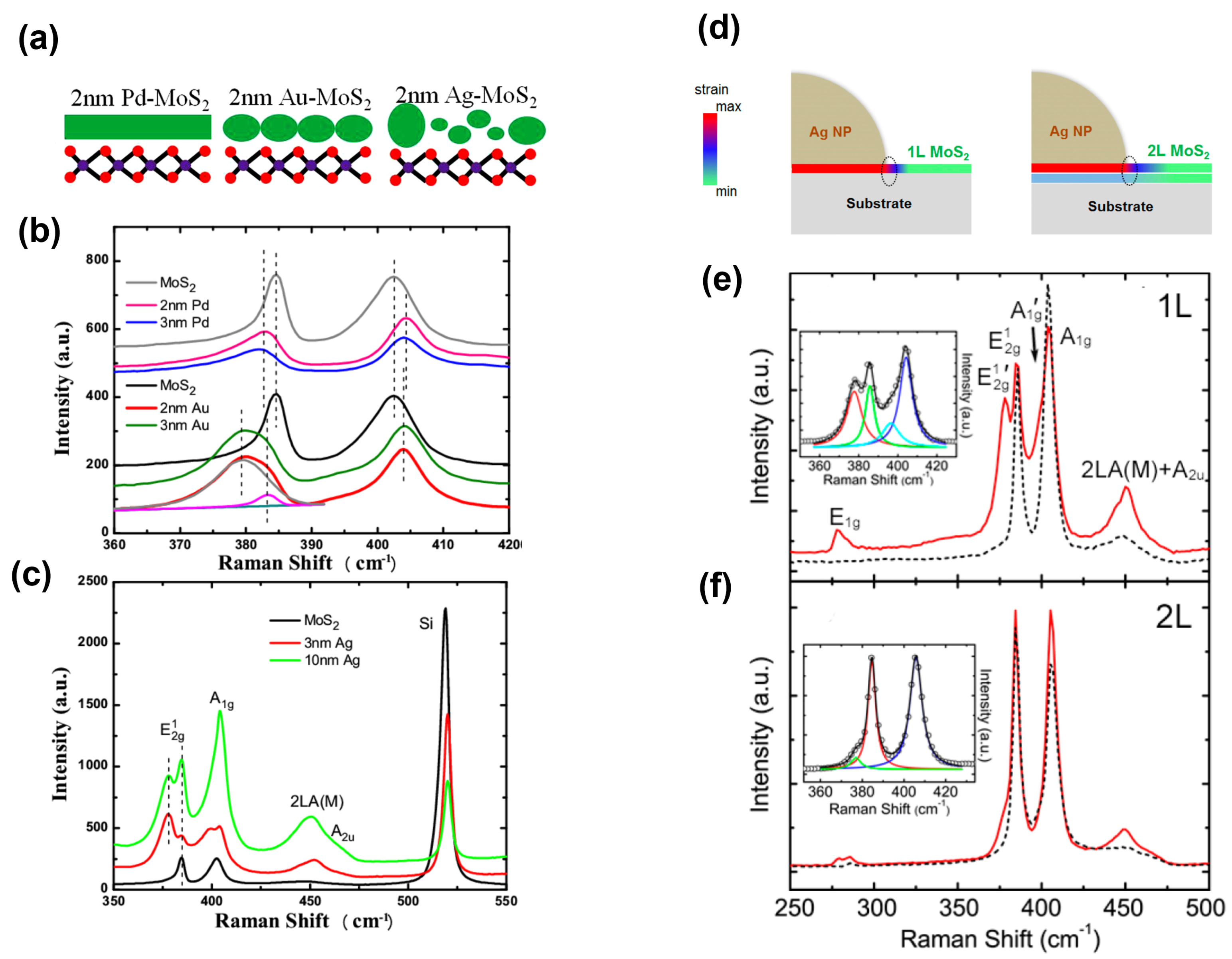
3.1. Metal Deposition on MoS
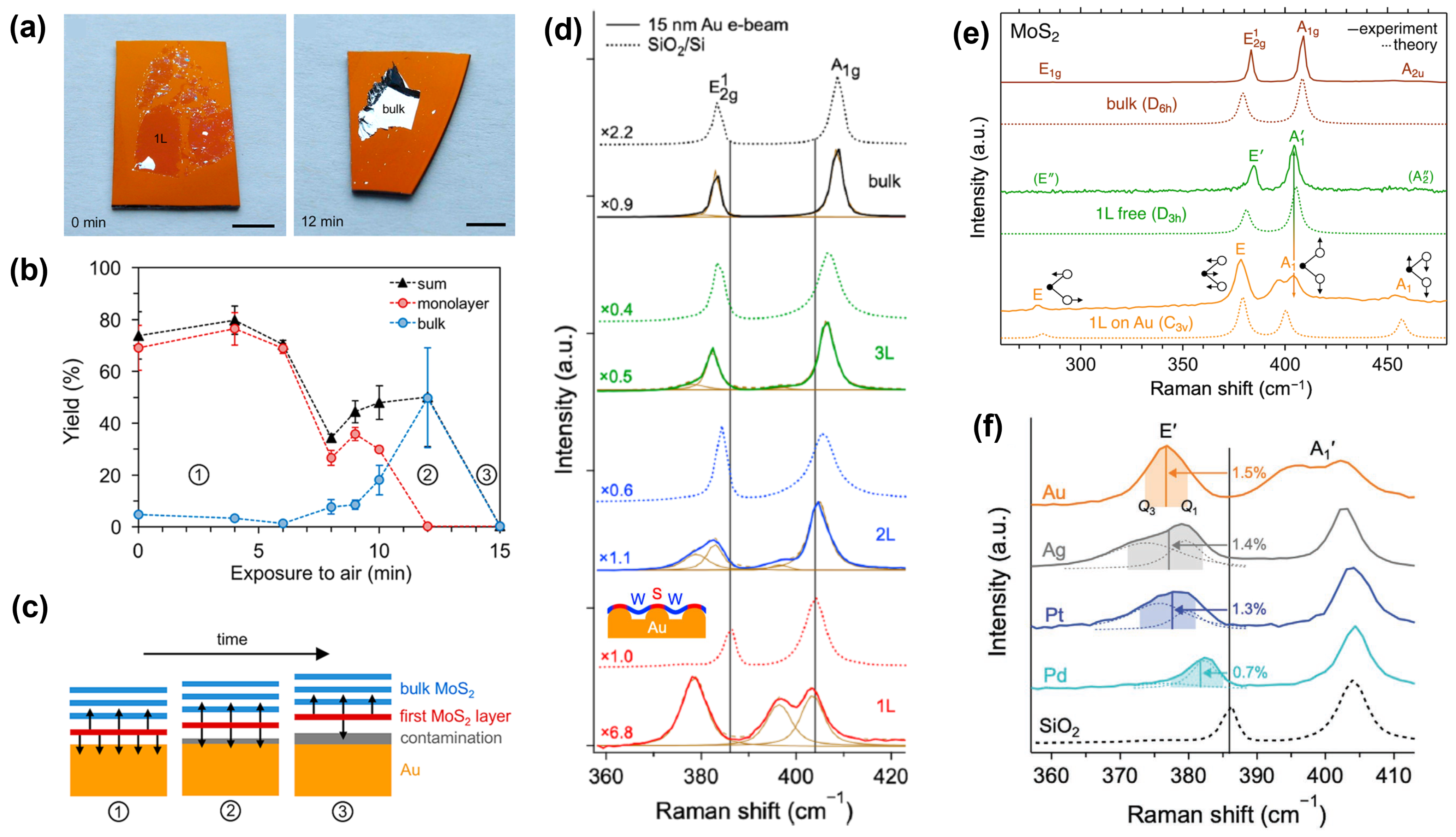
 2

In the first approach, the heterostructure is fabricated by depositing a metal film onto the MoS 2 surface. This approach is what is normally used to make metal contacts for electronic devices. The deposition is typically performed by evaporation under vacuum onto exfoliated or CVD-grown MoS 2 flakes supported by SiO 2 .
Gong et al. [35] studied the effect on mono-layer MoS 2 of the contact with three different metals, namely, Pd, Au, and Ag. All three metallic films have the same average thickness, i.e., 2 nm, but their morphology is different: Pd forms a smooth film that wets MoS 2 uniformly, whereas Au and Ag form rougher films, showing a tendency to agglomerate in nanoclusters (Figure 3a). The Raman spectra of the Pd- and Au-covered mono-layer MoS 2 (Figure 3b) show an upward shift of the A 1 g mode and a downshift of E 2 g 1 . The former is attributed to the increased stiffness of the vertical vibration of S atoms due to the interaction with the metal. The latter is associated with the combined effect of two different contributions: the enhanced electron screening provided by the metal, which weakens the planar interionic interaction, and the in-plane metal-induced strain that occurs where MoS 2 is in close contact with the metallic film or clusters. The strain effect depends on the homogeneity of the contact between metal and MoS 2 and thus on the film morphology at the metal-MoS 2 interface. The nonuniform morphology of the Au and Ag films produces regions of different contact with MoS 2 . The E 2 g 1 splitting observed for Au and Ag (Figure 3b,c, see the vertical dashed lines and the two fitting components of the 2 nm-Au curve) is explained as being due to two different contact regions of the metal-MoS 2 nonuniform interface. While the whole MoS 2 flake is screened by the metal film, resulting in the softening of E , the parts of MoS 2 under closer contact with the metal are strained, producing further softening of the same mode, which results in an additional peak at lower frequency.
Similar interpretations based on local strain at nonuniform interfaces are also adopted in other works to qualitatively explain the splitting of the E mode in metal-covered mono-layer MoS 2 [36,55]. Sun et al. observed such a splitting in Raman spectra of 5 nm-sized Ag nanoparticles deposited on mono-layer MoS 2 (Figure 3d,e). In this case, E 2 g 1 and A 1 g peaks of Ag/MoS 2 remain at the same positions as pristine MoS 2 (Figure 3e). However, two new peaks downshift from E 2 g 1 and A 1 g modes (labeled as E 2 g 1 and A 1 g in Figure 3e, see also inset). In mono-layer Ag/MoS 2 (Figure 3e), the downshifts of E 2 g 1 and A 1 g are ∼8 and ∼7.9 cm 1 from E 2 g 1 and A 1 g , respectively. They attributed the origin of these new peaks to the local strain of MoS 2 at the boundary of Ag nanoparticles. The strain-induced Raman peaks are enhanced by the strong electric field at the metal-MoS 2 boundary, produced by the Ag surface plasmon excitation. The relative intensity of these peaks becomes much weaker in thicker MoS 2 flakes (Figure 3f) because the Raman signals from the less-strained lower layers are also locally enhanced by the plasmon resonance, and they dominate the signal from the strained top layer (Figure 3d).
The study of junctions fabricated via metal deposition on MoS 2 is useful to understand the properties of contacts in MoS 2 devices since it relies on the same fabrication process. However, this method does not offer high control on the interface morphology, critically depending on metal wettability and deposition parameters. The resulting nonuniform metal-MoS 2 contact complicates the interpretation of Raman features and accounts for the poor consistency among the studies based on this approach.

3.2. MoS 2 Exfoliation on Metals

In the second approach, MoS 2 layers are deposited on a metal surface through mechanical exfoliation of a bulk crystal. Recent works have shown that this method can be used to produce large-area mono-layer MoS 2 films [13,14,15,16]. Velick y ´ et al. [15] demonstrated that the mechanical exfoliation of MoS 2 on gold produces mono-layer flakes up to a centimeter scale. The effectiveness of this technique critically depends on the cleanliness and smoothness of the Au surface. As shown in Figure 4a,b, the average area percentage of mono-layer MoS 2 is 70-80% on freshly cleaned Au but strongly decreases as the Au surface is exposed to air for a few minutes. Concurrently, the proportion of bulk flakes increases. The exfoliation of a single MoS 2 layer is facilitated by the stronger van der Waals (vdW) interaction with Au, compared to the interlayer vdW interaction in bulk MoS 2 . However, the Au-MoS 2 interaction becomes weaker for increasing air exposure because the Au surface gets covered by airborne contaminants (Figure 4c). A similar trend is observed for increasing surface roughness, due to the decrease in the contact area between Au and the first MoS 2 layer, which reduces their mutual interaction.
In a follow-up paper by the same group [37], the vibrational properties of MoS 2 exfoliated on Au were studied by conventional and tip-enhanced Raman spectroscopy (TERS). The Raman spectra reported in Figure 4d show the comparison between MoS 2 /Au and MoS 2 /SiO 2 for different MoS 2 thicknesses. In mono-layer MoS 2 /Au (red solid line), the in-plane E mode downshifts and broadens compared to MoS 2 /SiO 2 (red dotted line), while the A 1 mode shows two components: a low-frequency peak ( A 1 ( L ) ) at 396.4 ± 0.3 cm 1 , and a high-frequency one ( A 1 ( H ) ) at 403.7 ± 0.2 cm 1 , i.e., approximately the same frequency of A 1 in MoS 2 /SiO 2 . These Raman features are interpreted in terms of a nonuniform contact between MoS 2 and Au, due to the roughness of the Au surface (see the schematic inset in Figure 4d). The heterogeneous contact leads to a biaxial tensile strain distribution between 0.6% and 1.9%, causing the downshift and broadening of E (centered at 378.2 ± 0.6 cm 1 ). The A 1 ( L ) component is attributed to n-type doping of the MoS 2 regions, which strongly interact with the Au substrate, whereas the A 1 ( H ) component is the contribution coming from the suspended and undoped MoS 2 regions (see inset at the bottom of Figure 4d). The interaction with Au only produces significant effects in the first MoS 2 layer. Bi-layer MoS 2 (blue line in Figure 4d) is only partially affected by the Au substrate, while for more than three layers the effects of strain and doping are irrelevant and the spectra are very similar to MoS 2 /SiO 2 .
The strong interaction with Au lowers the symmetry of mono-layer MoS 2 from D 3 h to C 3 v , due to the breaking of the reflection symmetry in the basal MoS 2 plane. This change of symmetry activates the geometry-forbidden E Raman mode at ∼280 cm 1 and the symmetry-forbidden A 2 IR mode at ∼455 cm 1 (Figure 4e) [38]. As shown in Figure 4e, these modes are undetected in quasi-freestanding mono-layer MoS 2 and for thicker MoS 2 crystals (the visibility of these modes in bulk MoS 2 can be attributed to resonance effects).
The exfoliation of MoS 2 on other metals has been also investigated [39]. These experiments showed that gold is the best substrate in terms of the lateral size of the mono-layer flakes. A moderate exfoliation yield is achieved for other precious metals, including Pt, Pd, and Ag, while hardly any exfoliated material is found on base metals, such as Cu, Ni, Co, Cr, and Ti. This result depends on the ability of a metal to resist oxidation because the surface oxide layers reduces the MoS 2 -metal binding strength. The exfoliation yield also correlates to the interfacial strain, which is inferred from the downshift of E observed in the Raman spectra of Figure 4f. Despite its relatively high propensity to oxidation, Ag was found to have a larger exfoliation yield than Pd and Pt. This result is attributed to the larger tensile strain of MoS 2 on Ag, which might facilitate a mechanical pinning of the first MoS 2 layer to the Ag surface.
The origin of the splitting of the A 1 mode has been the subject of debate. In the works we discussed so far, n-type doping induced by the metal contact is considered responsible for the presence of a low-frequency component of A 1 . However, other authors have proposed different interpretations. Pollmann et al. [16] used the exfoliation technique to study the MoS 2 /Au interface on polycrystalline Au films and Au(111) single crystals. The Raman spectrum of mono-layer MoS 2 shows the E 2 g 1 mode at 379 cm 1 , downshifted compared to MoS 2 on SiO 2 due to tensile strain in the MoS 2 lattice. The A 1 g mode is split, with a low-frequency component ( A 1 g r e d u c e d ) at 397 cm 1 and the other one at approximately the same frequency as in MoS 2 /SiO 2 . To verify that the A 1 g r e d u c e d mode is an A-type MoS 2 Raman mode, they performed polarization-dependent Raman spectroscopy and found that this mode behaves like the A 1 g mode, when changing from a parallel-polarized configuration (xx) to a cross-polarized configuration (xy) [22]. The intensity ratio A 1 g r e d u c e d / A 1 g increases with the smoothness of the Au surface. The ratio is highest for the mono-layer MoS 2 on the very smooth surface of the Au(111) single crystal and decreases as the Au surface becomes rougher. Therefore, the emergence of the A 1 g r e d u c e d mode is caused by the direct MoS 2 -Au contact. However, Kelvin probe force microscopy (KPFM) measurements do not support the hypothesis of n-type doping as the main cause for the downshift of the A 1 g mode. X-ray photoelectron spectroscopy (XPS) data provide evidence for the emergence of mid gap states due to a sulfur-mediated spreading of Mo d orbitals into the band gap. As previously predicted by Gong et al. [19], this effect causes Fermi level pinning and weakens the Mo-S bond. The origin of the low-frequency A 1 g mode is thus attributed to the electron occupation of mid gap states, which weakens the Mo-S bond in the region of close contact between Au and MoS 2 .

3.3. Growth of MoS 2 on Metal Substrates

The two fabrication approaches described above produce metal-MoS 2 interfaces that are likely to form nonuniform contact between the metal film and the MoS 2 layer, due to surface roughness and airborne contaminants. Exfoliation onto the atomically flat surface of a metal single crystal tackles the roughness issue but makes the identification of MoS 2 flakes by optical microscopy more problematic. Growing MoS 2 directly on a metal surface is an alternative approach that can produce mono-layer MoS 2 in a controlled atmosphere, reducing the contamination level and ensuring a uniform MoS 2 -metal interface. Different techniques have been studied to synthesize MoS 2 layers on metals. For instance, CVD in a furnace apparatus has been shown to be a viable route to grow mono-layer MoS 2 on Au, starting from MoO 3 and S precursors [17,40]. A different CVD method, based on Mo deposition in a H 2 S atmosphere, has been originally developed by the Besenbacher’s group [57] and extensively used to prepare mono-layer MoS 2 on Au(111) under ultra-high vacuum (UHV) conditions for surface science investigations [18,58,59,60]. Recently, we reported on the fabrication of the cm-scale mono-layer MoS 2 on Au(111) and Ag(111) by pulsed laser deposition (PLD) in UHV, an alternative physical vapor deposition (PVD) approach that allowed us to study MoS 2 and MoS 2 /WS 2 heterostructures by scanning tunneling microscopy (STM) and Raman spectroscopy [41,42,43,61].
STM studies of mono-layer MoS 2 on Au(111) show a moiré superstructure due to the lattice mismatch between MoS 2 (3.16 Å in-plane lattice constant) and Au(111) (2.89 Å) (Figure 5a,b). Low-energy electron diffraction (LEED) patterns revealed that the MoS 2 lattice is aligned to the high-symmetry directions of Au(111) and the mismatch causes 10 MoS 2 unit cell to coincide with 11 Au(111) cells, generating a long-range ordered hexagonal moiré superlattice [18]. The moiré unit cell (black line in Figure 5b) contains three regions with different stackings of MoS 2 on the top Au layer: one top-site and two hollow-site alignments, corresponding to fcc and hcp stackings. The stacking geometry affects the local equilibrium distance and therefore the local interaction between MoS 2 and Au, also resulting in a modulation of the local electronic properties [60]. The moiré periodicity measured by STM is ∼3.2 nm [18,58,60]. The 10/11 MoS 2 /Au coincidence therefore imposes a ∼1% biaxial tensile strain on MoS 2 , in agreement with STM measurements of a ∼3.2 Å MoS 2 lattice parameter, which is slightly larger than the relaxed value.
Yasuda et al. [40] proposed that the stacking variation in the moiré unit cell is the origin of the A 1 mode splitting. They deposited mono-layer MoS 2 on Au(111) and polycrystalline Au by CVD, using MoS 2 and S powders as precursors in a quartz furnace. The corresponding Raman spectra are shown in Figure 5c, compared to the spectrum of CVD MoS 2 on SiO 2 . In MoS 2 /Au(111), besides the downshift of E 2 g 1 , the splitting of the A 1 g mode is resolved, with a low-frequency component ( A 1 g I ) at 398 cm 1 and a high-frequency one ( A 1 g I I ) at 403 cm 1 . Notably, the A 1 g mode of MoS 2 on polycrystalline Au is not split, and its intensity is comparable to that of E 2 g 1 , in contrast to the lower relative intensity of the two A 1 g components in MoS 2 /Au(111). Electrochemical Raman spectra were acquired under different potentials to investigate the dependence of the Raman modes on doping. As shown in Figure 5d, the peak frequency of the Raman modes of MoS 2 /Au(111) does not change significantly with the applied potential, suggesting that the A 1 splitting is not a doping effect but is rather related to strain. Since the A 1 mode does not split on polycrystalline Au, the authors argued that the strain is associated with the specific stacking registry between MoS 2 and Au(111), which periodically varies in the moiré pattern. In particular, the stronger hybridization of S atoms in the on-top positions locally affects the S-Au bond, introducing an out-of-plane strain component that ultimately results in the observed splitting of the A 1 mode.
The growth of MoS 2 under UHV conditions on atomically flat and clean single-crystal metal surfaces is the ideal way to achieve a homogeneous MoS 2 -metal interface, suitable for fundamental studies. However, Raman spectroscopy is not a typical surface science technique, and its application to the study of UHV-grown MoS 2 /metal systems is still limited to a few works [41,42,43,63]. We recently combined UHV STM with ex-situ Raman spectroscopy to study the surface and interface properties of mono-layer MoS 2 grown on Au(111) and Ag(111) by PLD [41,42]. Two representative STM images of our PLD-grown MoS 2 /Au(111) are reported in Figure 5a,b, showing the well-ordered moiré pattern and high surface quality of the MoS 2 layer. In agreement with previous works, the Raman spectrum (Figure 5e) shows the E mode centered at 378 cm 1 , and the A 1 mode split in two components (396 and 403 cm 1 ).
It is important to notice that Raman spectra of MoS 2 grown on metals can be affected by lateral confinement effects. As discussed in Section 2 regarding the Raman response of defective MoS 2 , the lateral confinement breaks the long-range crystalline order and relaxes the fundamental Raman selection rule q 0 , where q is the phonon wavevector. As a result, the contribution of phonon states away from the zone center and the dispersion of phonon bands can influence the Raman spectrum. Depending on the growth technique, the size of crystalline domains and the defect density can vary significantly. On Au(111) or Ag(111), the MoS 2 lattice can grow in two different crystallographic orientations, and domain boundaries are commonly observed between differently oriented domains. The linear size of such domains can be as small as few tens nanometers, as observed for instance in PLD-grown MoS 2 on Au(111) [41].
Ag(111) has almost the same surface structure as Au(111), with Au and Ag being both fcc crystals with 4.065 and 4.079 Å lattice constants, respectively [64]. As a result, mono-layer MoS 2 on Ag(111) has the same structural features as on Au(111), with a characteristic hexagonal moiré pattern showing the same appearance and periodicity in STM data [42]. The corresponding Raman spectrum is shown in the top panel of Figure 5f. The E mode is at 377 cm 1 , and the A 1 mode is centered at 400 cm 1 . In this case, we do not observe a clear splitting of the A 1 mode, as highlighted by the Voigt fitting of the peak. We note, however, that the peak position approximately corresponds to the average position of the two A 1 components of MoS 2 /Au(111). This Raman spectrum (Figure 5f, top panel) has been measured immediately after the sample exposure to air. Surprisingly, the spectrum changes with increasing exposure time to air, as shown in the other three panels of Figure 5f. After just a few hours of air exposure, the A 1 mode starts shifting upward and becoming relatively more intense. The E mode develops a second component at higher frequency ( E ( 2 ) green curve) that gradually upshifts, while the low-frequency component ( E ( 1 ) ) maintains its original position. The upshift of Raman modes and the increase in A 1 / E intensity ratio suggest that the exposure to ambient conditions weakens the MoS 2 -Ag interaction. The coexistence of two contributions, E ( 1 ) and E ( 2 ) , to the in-plane vibration can be attributed to the simultaneous sampling of regions where MoS 2 strongly interacts with Ag and regions where such interactions are weaker. The gradual intensity decrease in E ( 1 ) against E ( 2 ) suggests that the regions of weak interaction become predominant with increasing air exposure time. With the support of further Raman and XPS data, we proposed that this aging effect is caused by water intercalation at the MoS 2 /Ag interface, which reduces the interaction between MoS 2 and Ag. Therefore, the ambient conditions may significantly affect the interface between MoS 2 and metals over a relatively short time, and care must be taken in Raman studies of these systems to reduce the influence of air exposure on the recorded spectra.
In conclusion of this Section, Table 1 summarizes the positions of the E and A 1 modes of mono-layer MoS 2 reported in some of the discussed MoS 2 -metal heterosystems.

4. Conclusions and Perspectives

Raman spectroscopy studies of MoS 2 interacting with metals show remarkable differences compared to freestanding MoS 2 . The contact with metals modifies the MoS 2 structural and electronic properties, and this influence has profound effects on the vibrational modes. The impact of these effects on Raman spectra depends on the characteristics of the metal-MoS 2 interface and therefore on the fabrication technique used to produce the heterosystem. The MoS 2 -Au heterosystem has been one of the most studied so far, partly because exfoliation of MoS 2 on a clean Au surface produces mono-layer flakes of relatively large area. The interaction with Au affects the in-plane E and the out-of-plane A 1 vibrational modes, and it breaks the reflection symmetry in the basal MoS 2 plane, thus activating modes that are silent in freestanding mono-layer MoS 2 . The E mode typically downshifts by 5-6 cm 1 , compatibly with an average ∼1% in-plane biaxial tensile strain induced by Au. The A 1 mode shows a lower relative intensity and an intriguing splitting whose origin is still debated. These variations make impossible to infer the number of layers in MoS 2 interacting with metals, by using the well-known relation between the frequency distance of the two main Raman modes and the MoS 2 thickness.
Raman investigations of model systems are necessary to understand in detail the physical mechanisms behind the anomalous Raman spectra. The synthesis of mono-layer MoS 2 on single-crystal metal surfaces under UHV conditions is the most promising fabrication approach to produce morphologically uniform and atomically clean MoS 2 -metal interfaces for fundamental studies. In addition to traditional UHV surface science techniques, this approach would benefit from the integration of in situ Raman spectroscopy as the air exposure of MoS 2 -metal samples can alter the interface due to the intercalation of contaminants. The experimental work should be complemented by theoretical investigations of metal-supported MoS 2 . While the theoretical modeling of freestanding MoS 2 is well-established, the calculation of Raman spectra of metal-supported MoS 2 has been addressed by very few works [38,65]. As different effects may contribute to the anomalous behavior of Raman modes, theoretical calculations are necessary to disentangle such contributions and provide quantitative insight into the interpretation of Raman spectra.
The effects of the interaction with metals discussed in this review are not limited to MoS 2 but are common to the other semiconducting TMDs. Raman studies of 2D MoS 2 interacting with metals can access the interface properties of TMD-metal systems and inform the design of efficient metal contacts as well as the development of metal-assisted synthesis methods.

Author Contributions

Conceptualization, F.T.; writing—original draft preparation, F.T.; writing—review and editing, F.T., P.D., V.R., A.L.B. and C.S.C.; supervision, V.R., A.L.B. and C.S.C.; and funding acquisition, C.S.C. and A.L.B. All authors have read and agreed to the published version of the manuscript.

Funding

V. Russo, A. Li Bassi and C.S. Casari acknowledge funding by the project funded under the National Recovery and Resilience Plan (NRRP), Mission 4 Component 2 Investment 1.3—Call for tender No. 1561 of 11.10.2022 of Ministero dell’Università e della Ricerca (MUR), and by the European Union—NextGenerationEU. Award Number: Project code PE0000021, Concession Decree No. 1561 of 11.10.2022 adopted by Ministero dell’Università e della Ricerca (MUR), CUP D43C22003090001, project title “Network 4 Energy Sustainable Transition—NEST”. The authors acknowledge partial funding from the European Research Council (ERC) under the European Union’s Horizon 2020 research and innovation program ERC Consolidator Grant (ERC CoG2016 EspLORE grant agreement no. 724610, website: www.esplore.polimi.it).

Conflicts of Interest

The authors declare no conflict of interest.

References

  1. Wang, Q.H.; Kalantar-Zadeh, K.; Kis, A.; Coleman, J.N.; Strano, M.S. Electronics and optoelectronics of two-dimensional transition metal dichalcogenides. Nat. Nanotechnol. 2012, 7, 699–712. [Google Scholar] [CrossRef] [PubMed]
  2. Manzeli, S.; Ovchinnikov, D.; Pasquier, D.; Yazyev, O.V.; Kis, A. 2D transition metal dichalcogenides. Nat. Rev. Mater. 2017, 2, 17033. [Google Scholar] [CrossRef]
  3. Jariwala, D.; Sangwan, V.K.; Lauhon, L.J.; Marks, T.J.; Hersam, M.C. Emerging device applications for semiconducting two-dimensional transition metal dichalcogenides. ACS Nano 2014, 8, 1102–1120. [Google Scholar] [CrossRef] [PubMed]
  4. Xu, X.; Yao, W.; Xiao, D.; Heinz, T.F. Spin and pseudospins in layered transition metal dichalcogenides. Nat. Phys. 2014, 10, 343–350. [Google Scholar] [CrossRef]
  5. Mak, K.F.; Shan, J. Photonics and optoelectronics of 2D semiconductor transition metal dichalcogenides. Nat. Photonics 2016, 10, 216–226. [Google Scholar] [CrossRef]
  6. Cao, Y. Roadmap and direction toward high-performance MoS2 hydrogen evolution catalysts. ACS Nano 2021, 15, 11014–11039. [Google Scholar] [CrossRef]
  7. Chhowalla, M.; Shin, H.S.; Eda, G.; Li, L.J.; Loh, K.P.; Zhang, H. The chemistry of two-dimensional layered transition metal dichalcogenide nanosheets. Nat. Chem. 2013, 5, 263–275. [Google Scholar] [CrossRef]
  8. Duan, X.; Wang, C.; Pan, A.; Yu, R.; Duan, X. Two-dimensional transition metal dichalcogenides as atomically thin semiconductors: Opportunities and challenges. Chem. Soc. Rev. 2015, 44, 8859–8876. [Google Scholar] [CrossRef]
  9. Choi, W.; Choudhary, N.; Han, G.H.; Park, J.; Akinwande, D.; Lee, Y.H. Recent development of two-dimensional transition metal dichalcogenides and their applications. Mater. Today 2017, 20, 116–130. [Google Scholar] [CrossRef]
  10. Ganatra, R.; Zhang, Q. Few-layer MoS2: A promising layered semiconductor. ACS Nano 2014, 8, 4074–4099. [Google Scholar] [CrossRef]
  11. Mak, K.F.; Lee, C.; Hone, J.; Shan, J.; Heinz, T.F. Atomically thin MoS2: A new direct-gap semiconductor. Phys. Rev. Lett. 2010, 105, 136805. [Google Scholar] [CrossRef] [PubMed]
  12. Radisavljevic, B.; Radenovic, A.; Brivio, J.; Giacometti, V.; Kis, A. Single-layer MoS2 transistors. Nat. Nanotechnol. 2011, 6, 147–150. [Google Scholar] [CrossRef] [PubMed]
  13. Magda, G.Z.; Peto, J.; Dobrik, G.; Hwang, C.; Biró, L.P.; Tapasztó, L. Exfoliation of large-area transition metal chalcogenide single layers. Sci. Rep. 2015, 5, 14714. [Google Scholar] [CrossRef] [PubMed]
  14. Desai, S.B.; Madhvapathy, S.R.; Amani, M.; Kiriya, D.; Hettick, M.; Tosun, M.; Zhou, Y.; Dubey, M.; Ager, J.W., III; Chrzan, D.; et al. Gold-mediated exfoliation of ultralarge optoelectronically-perfect monolayers. Adv. Mater. 2016, 28, 4053–4058. [Google Scholar] [CrossRef] [PubMed]
  15. Velickỳ, M.; Donnelly, G.E.; Hendren, W.R.; McFarland, S.; Scullion, D.; DeBenedetti, W.J.; Correa, G.C.; Han, Y.; Wain, A.J.; Hines, M.A.; et al. Mechanism of gold-assisted exfoliation of centimeter-sized transition-metal dichalcogenide monolayers. ACS Nano 2018, 12, 10463–10472. [Google Scholar] [CrossRef]
  16. Pollmann, E.; Sleziona, S.; Foller, T.; Hagemann, U.; Gorynski, C.; Petri, O.; Madauß, L.; Breuer, L.; Schleberger, M. Large-area, two-dimensional MoS2 exfoliated on gold: Direct experimental access to the metal–semiconductor interface. ACS Omega 2021, 6, 15929–15939. [Google Scholar] [CrossRef]
  17. Yang, P.; Zhang, S.; Pan, S.; Tang, B.; Liang, Y.; Zhao, X.; Zhang, Z.; Shi, J.; Huan, Y.; Shi, Y.; et al. Epitaxial growth of centimeter-scale single-crystal MoS2 monolayer on Au(111). ACS Nano 2020, 14, 5036–5045. [Google Scholar] [CrossRef]
  18. Bana, H.; Travaglia, E.; Bignardi, L.; Lacovig, P.; Sanders, C.E.; Dendzik, M.; Michiardi, M.; Bianchi, M.; Lizzit, D.; Presel, F.; et al. Epitaxial growth of single-orientation high-quality MoS2 monolayers. 2D Mater. 2018, 5, 035012. [Google Scholar] [CrossRef]
  19. Gong, C.; Colombo, L.; Wallace, R.M.; Cho, K. The unusual mechanism of partial Fermi level pinning at metal–MoS2 interfaces. Nano Lett. 2014, 14, 1714–1720. [Google Scholar] [CrossRef]
  20. Bruix, A.; Miwa, J.A.; Hauptmann, N.; Wegner, D.; Ulstrup, S.; Grønborg, S.S.; Sanders, C.E.; Dendzik, M.; Čabo, A.G.; Bianchi, M.; et al. Single-layer MoS2 on Au(111): Band gap renormalization and substrate interaction. Phys. Rev. B 2016, 93, 165422. [Google Scholar] [CrossRef]
  21. Blue, B.T.; Jernigan, G.G.; Le, D.; Fonseca, J.J.; Lough, S.D.; Thompson, J.E.; Smalley, D.D.; Rahman, T.S.; Robinson, J.T.; Ishigami, M. Metallicity of 2H-MoS2 induced by Au hybridization. 2D Mater. 2020, 7, 025021. [Google Scholar] [CrossRef]
  22. Zhang, X.; Qiao, X.F.; Shi, W.; Wu, J.B.; Jiang, D.S.; Tan, P.H. Phonon and Raman scattering of two-dimensional transition metal dichalcogenides from monolayer, multilayer to bulk material. Chem. Soc. Rev. 2015, 44, 2757–2785. [Google Scholar] [CrossRef] [PubMed]
  23. Lee, J.U.; Park, J.; Son, Y.W.; Cheong, H. Anomalous excitonic resonance Raman effects in few-layered MoS2. Nanoscale 2015, 7, 3229–3236. [Google Scholar] [CrossRef]
  24. Luo, X.; Zhao, Y.; Zhang, J.; Xiong, Q.; Quek, S.Y. Anomalous frequency trends in MoS2 thin films attributed to surface effects. Phys. Rev. B 2013, 88, 075320. [Google Scholar] [CrossRef]
  25. Li, H.; Zhang, Q.; Yap, C.C.R.; Tay, B.K.; Edwin, T.H.T.; Olivier, A.; Baillargeat, D. From bulk to monolayer MoS2: Evolution of Raman scattering. Adv. Funct. Mater. 2012, 22, 1385–1390. [Google Scholar] [CrossRef]
  26. Scheuschner, N.; Gillen, R.; Staiger, M.; Maultzsch, J. Interlayer resonant Raman modes in few-layer MoS2. Phys. Rev. B 2015, 91, 235409. [Google Scholar] [CrossRef]
  27. Conley, H.J.; Wang, B.; Ziegler, J.I.; Haglund, R.F., Jr.; Pantelides, S.T.; Bolotin, K.I. Bandgap engineering of strained monolayer and bilayer MoS2. Nano Lett. 2013, 13, 3626–3630. [Google Scholar] [CrossRef]
  28. Rice, C.; Young, R.; Zan, R.; Bangert, U.; Wolverson, D.; Georgiou, T.; Jalil, R.; Novoselov, K. Raman-scattering measurements and first-principles calculations of strain-induced phonon shifts in monolayer MoS2. Phys. Rev. B 2013, 87, 081307. [Google Scholar] [CrossRef]
  29. Lloyd, D.; Liu, X.; Christopher, J.W.; Cantley, L.; Wadehra, A.; Kim, B.L.; Goldberg, B.B.; Swan, A.K.; Bunch, J.S. Band gap engineering with ultralarge biaxial strains in suspended monolayer MoS2. Nano Lett. 2016, 16, 5836–5841. [Google Scholar] [CrossRef]
  30. Chang, C.H.; Fan, X.; Lin, S.H.; Kuo, J.L. Orbital analysis of electronic structure and phonon dispersion in MoS2, MoSe2, WS2, and WSe2 monolayers under strain. Phys. Rev. B 2013, 88, 195420. [Google Scholar] [CrossRef]
  31. Shi, H.; Pan, H.; Zhang, Y.W.; Yakobson, B.I. Quasiparticle band structures and optical properties of strained monolayer MoS2 and WS2. Phys. Rev. B 2013, 87, 155304. [Google Scholar] [CrossRef]
  32. Kukucska, G.; Koltai, J. Theoretical investigation of strain and doping on the Raman spectra of monolayer MoS2. Phys. Status Solidi (b) 2017, 254, 1700184. [Google Scholar] [CrossRef]
  33. Chakraborty, B.; Bera, A.; Muthu, D.; Bhowmick, S.; Waghmare, U.V.; Sood, A. Symmetry-dependent phonon renormalization in monolayer MoS2 transistor. Phys. Rev. B 2012, 85, 161403. [Google Scholar] [CrossRef]
  34. Mignuzzi, S.; Pollard, A.J.; Bonini, N.; Brennan, B.; Gilmore, I.S.; Pimenta, M.A.; Richards, D.; Roy, D. Effect of disorder on Raman scattering of single-layer MoS2. Phys. Rev. B 2015, 91, 195411. [Google Scholar] [CrossRef]
  35. Gong, C.; Huang, C.; Miller, J.; Cheng, L.; Hao, Y.; Cobden, D.; Kim, J.; Ruoff, R.S.; Wallace, R.M.; Cho, K.; et al. Metal contacts on physical vapor deposited monolayer MoS2. ACS Nano 2013, 7, 11350–11357. [Google Scholar] [CrossRef] [PubMed]
  36. Sun, Y.; Liu, K.; Hong, X.; Chen, M.; Kim, J.; Shi, S.; Wu, J.; Zettl, A.; Wang, F. Probing local strain at MX2–metal boundaries with surface plasmon-enhanced Raman scattering. Nano Lett. 2014, 14, 5329–5334. [Google Scholar] [CrossRef] [PubMed]
  37. Velickỳ, M.; Rodriguez, A.; Bousa, M.; Krayev, A.V.; Vondracek, M.; Honolka, J.; Ahmadi, M.; Donnelly, G.E.; Huang, F.; Abruña, H.D.; et al. Strain and charge doping fingerprints of the strong interaction between monolayer MoS2 and gold. J. Phys. Chem. Lett. 2020, 11, 6112–6118. [Google Scholar] [CrossRef]
  38. Rodriguez, A.; Velickỳ, M.; Řáhová, J.; Zólyomi, V.; Koltai, J.; Kalbáč, M.; Frank, O. Activation of Raman modes in monolayer transition metal dichalcogenides through strong interaction with gold. Phys. Rev. B 2022, 105, 195413. [Google Scholar] [CrossRef]
  39. Velickỳ, M.; Donnelly, G.E.; Hendren, W.R.; DeBenedetti, W.J.; Hines, M.A.; Novoselov, K.S.; Abruña, H.D.; Huang, F.; Frank, O. The intricate love affairs between MoS2 and metallic substrates. Adv. Mater. Interfaces 2020, 7, 2001324. [Google Scholar] [CrossRef]
  40. Yasuda, S.; Takahashi, R.; Osaka, R.; Kumagai, R.; Miyata, Y.; Okada, S.; Hayamizu, Y.; Murakoshi, K. Out-of-plane strain induced in a moiré superstructure of monolayer MoS2 and MoSe2 on Au(111). Small 2017, 13, 1700748. [Google Scholar] [CrossRef]
  41. Tumino, F.; Casari, C.S.; Passoni, M.; Russo, V.; Li Bassi, A. Pulsed laser deposition of single-layer MoS2 on Au(111): From nanosized crystals to large-area films. Nanoscale Adv. 2019, 1, 643–655. [Google Scholar] [CrossRef] [PubMed]
  42. Tumino, F.; Grazianetti, C.; Martella, C.; Ruggeri, M.; Russo, V.; Li Bassi, A.; Molle, A.; Casari, C.S. Hydrophilic character of single-layer MoS2 grown on Ag (111). J. Phys. Chem. C 2021, 125, 9479–9485. [Google Scholar] [CrossRef] [PubMed]
  43. D’Agosta, P.; Tumino, F.; Russo, V.; Bassi, A.L.; Casari, C.S. Interface coupling in Au-supported MoS2–WS2 heterobilayers grown by pulsed laser deposition. Nanoscale 2023, 15, 7493–7501. [Google Scholar] [CrossRef] [PubMed]
  44. Zhou, K.G.; Withers, F.; Cao, Y.; Hu, S.; Yu, G.; Casiraghi, C. Raman modes of MoS2 used as fingerprint of van der Waals interactions in 2-D crystal-based heterostructures. ACS Nano 2014, 8, 9914–9924. [Google Scholar] [CrossRef] [PubMed]
  45. Wu, Y.; Song, X.; Zhou, X.; Song, R.; Tang, W.; Yang, D.; Wang, Y.; Lv, Z.; Zhong, W.; Cai, H.L.; et al. Piezo-Activated Atomic-Thin Molybdenum Disulfide/MXene Nanoenzyme for Integrated and Efficient Tumor Therapy via Ultrasound-Triggered Schottky Electric Field. Small 2023, 19, 2205053. [Google Scholar] [CrossRef]
  46. Ankitha, M.; Shabana, N.; Arjun, A.M.; Muhsin, P.; Rasheed, P.A. Ultrasensitive electrochemical detection of dopamine from human serum samples by Nb2CTx-MoS2 hetero structures. Microchem. J. 2023, 187, 108424. [Google Scholar] [CrossRef]
  47. Er, E.; Ateş, A.K. Design of an electrochemical sensing platform based on MoS2-PEDOT: PSS nanocomposite for the detection of epirubicin in biological samples. Microchem. J. 2023, 189, 108534. [Google Scholar] [CrossRef]
  48. Ribeiro-Soares, J.; Almeida, R.; Barros, E.B.; Araujo, P.T.; Dresselhaus, M.S.; Cançado, L.G.; Jorio, A. Group theory analysis of phonons in two-dimensional transition metal dichalcogenides. Phys. Rev. B 2014, 90, 115438. [Google Scholar] [CrossRef]
  49. Carvalho, B.R.; Malard, L.M.; Alves, J.M.; Fantini, C.; Pimenta, M.A. Symmetry-dependent exciton-phonon coupling in 2D and bulk MoS2 observed by resonance Raman scattering. Phys. Rev. Lett. 2016, 114, 136403, Erratum in Phys. Rev. Lett. 2016, 116, 089904. [Google Scholar] [CrossRef]
  50. Fan, J.H.; Gao, P.; Zhang, A.M.; Zhu, B.R.; Zeng, H.L.; Cui, X.D.; He, R.; Zhang, Q.M. Resonance Raman scattering in bulk 2H-MX2 (M = Mo, W; X = S, Se) and monolayer MoS2. J. Appl. Phys. 2014, 115, 053527. [Google Scholar] [CrossRef]
  51. Livneh, T.; Spanier, J.E. A comprehensive multiphonon spectral analysis in MoS2. 2D Mater. 2015, 2, 035003. [Google Scholar] [CrossRef]
  52. Carvalho, B.R.; Wang, Y.; Mignuzzi, S.; Roy, D.; Terrones, M.; Fantini, C.; Crespi, V.H.; Malard, L.M.; Pimenta, M.A. Intervalley scattering by acoustic phonons in two-dimensional MoS2 revealed by double-resonance Raman spectroscopy. Nat. Commun. 2017, 8, 14670. [Google Scholar] [CrossRef] [PubMed]
  53. Allain, A.; Kang, J.; Banerjee, K.; Kis, A. Electrical contacts to two-dimensional semiconductors. Nat. Mater. 2015, 14, 1195–1205. [Google Scholar] [CrossRef]
  54. Popov, I.; Seifert, G.; Tománek, D. Designing electrical contacts to MoS2 monolayers: A computational study. Phys. Rev. Lett. 2012, 108, 156802. [Google Scholar] [CrossRef]
  55. Yuan, H.; Cheng, G.; You, L.; Li, H.; Zhu, H.; Li, W.; Kopanski, J.J.; Obeng, Y.S.; Hight Walker, A.R.; Gundlach, D.J.; et al. Influence of metal–MoS2 interface on MoS2 transistor performance: Comparison of Ag and Ti contacts. ACS Appl. Mater. Interfaces 2015, 7, 1180–1187. [Google Scholar] [CrossRef]
  56. Sotthewes, K.; Van Bremen, R.; Dollekamp, E.; Boulogne, T.; Nowakowski, K.; Kas, D.; Zandvliet, H.J.; Bampoulis, P. Universal Fermi-level pinning in transition-metal dichalcogenides. J. Phys. Chem. C 2019, 123, 5411–5420. [Google Scholar] [CrossRef] [PubMed]
  57. Helveg, S.; Lauritsen, J.V.; Lægsgaard, E.; Stensgaard, I.; Nørskov, J.K.; Clausen, B.; Topsøe, H.; Besenbacher, F. Atomic-scale structure of single-layer MoS2 nanoclusters. Phys. Rev. Lett. 2000, 84, 951. [Google Scholar] [CrossRef]
  58. Sørensen, S.G.; Füchtbauer, H.G.; Tuxen, A.K.; Walton, A.S.; Lauritsen, J.V. Structure and electronic properties of in situ synthesized single-layer MoS2 on a gold surface. ACS Nano 2014, 8, 6788–6796. [Google Scholar] [CrossRef]
  59. Grønborg, S.S.; Ulstrup, S.; Bianchi, M.; Dendzik, M.; Sanders, C.E.; Lauritsen, J.V.; Hofmann, P.; Miwa, J.A. Synthesis of epitaxial single-layer MoS2 on Au(111). Langmuir 2015, 31, 9700–9706. [Google Scholar] [CrossRef]
  60. Krane, N.; Lotze, C.; Franke, K.J. Moiré structure of MoS2 on Au(111): Local structural and electronic properties. Surf. Sci. 2018, 678, 136–142. [Google Scholar] [CrossRef]
  61. Tumino, F.; Casari, C.S.; Li Bassi, A.; Tosoni, S. Nature of point defects in single-layer MoS2 supported on Au(111). J. Phys. Chem. C 2020, 124, 12424–12431. [Google Scholar] [CrossRef]
  62. Tumino, F.; Rabia, A.; Bassi, A.L.; Tosoni, S.; Casari, C.S. Interface-driven assembly of pentacene/MoS2 lateral heterostructures. J. Phys. Chem. C 2022, 126, 1132–1139. [Google Scholar] [CrossRef] [PubMed]
  63. do Amaral, G.M.; da Costa Tonon, I.; Román, R.J.P.; de Oliveira Plath, H.; Taniguchi, T.M.; de Lima, L.H.; Zagonel, L.F.; Landers, R.; de Siervo, A. Epitaxial growth, electronic hybridization and stability under oxidation of monolayer MoS2 on Ag(111). Appl. Surf. Sci. 2021, 538, 148138. [Google Scholar] [CrossRef]
  64. Davey, W.P. Precision measurements of the lattice constants of twelve common metals. Phys. Rev. 1925, 25, 753. [Google Scholar] [CrossRef]
  65. Sarkar, S.; Kratzer, P. Signatures of the Dichalcogenide–Gold Interaction in the Vibrational Spectra of MoS2 and MoSe2 on Au (111). J. Phys. Chem. C 2021, 125, 26645–26651. [Google Scholar] [CrossRef]
Figure 1. (a) Crystalline structure of 2H-MoS 2 . Top: Side view of a bi-layer structure. Bottom: top view. The black solid line marks the bulk unit cell. (b) Optical Raman active vibrational modes of bulk MoS 2 . E 1 g and E 2 g 1 correspond to in-plane vibrations and are doubly degenerate at Γ . A 1 g corresponds to out-of-plane vibrations of S atoms. (c) Evolution of Raman spectra for increasing number of MoS 2 layers (TL stands for tri-layer, i.e., an S-Mo-S layer). The peak positions of E 2 g 1 and A 1 g (green lines) are compared to theoretical calculations (red lines). Excitation wavelength: 532 nm. (d) Frequency shifts of A 1 g and (e) E 2 g 1 , as a function of the number of layers. (ce) reproduced with permission from ref. [24]. (f) Raman spectra and (g) A 1 g / E 2 g 1 intensity ratio of mono-, bi-, tri-layer, and bulk MoS 2 at different excitation energies. (f,g) reproduced with permission from ref. [49].
Crystals 13 01271 g001
Figure 2. (a) Schematics of the setup used to apply uniaxial tensile strain to MoS 2 in ref. [27]. (b) Raman spectra of mono-layer MoS 2 for increasing uniaxial tensile strain (excitation wavelength: 532 nm). (a,b) reproduced with permission from ref. [27]. (c) Top: schematics of the setup used to apply biaxial tensile strain to MoS 2 in ref. [29]. Bottom: optical micrograph of mono-layer MoS 2 crystals over an array of cylindrical microcavities. (d) Raman frequencies of A 1 g (top) and E 2 g 1 (bottom) as a function of biaxial tensile strain (excitation wavelength: 532 nm). (c,d) reproduced with permission from ref. [29]. (e) Schematics of the top-gated transistor used to modulate the electron concentration of mono-layer MoS 2 in ref. [33]. (f) Raman spectra of mono-layer MoS 2 for increasing electron doping level (excitation wavelength: 514.5 nm). Circles: experimental data; black lines: fits of Raman modes; red line: total fit. (e,f) reproduced with permission from ref. [33]. (g) Evolution of Raman spectra of mono-layer MoS 2 as a function of defect density (excitation wavelength: 532 nm). The asterisk refers to a Raman peak of the Si substrate. (h) Calculated phonon dispersion of E and A 1 [34]. (g,h) reproduced with permission from ref. [34].
Crystals 13 01271 g002
Figure 3. (a) Schematics of Pd, Au, and Ag film morphology on MoS 2 . (b) Raman spectra of MoS 2 covered by different thicknesses of Pd and Au, compared to pristine MoS 2 (grey and black lines). (c) Raman spectra of MoS 2 covered by different thicknesses of Ag, compared to pristine MoS 2 (black line) (excitation wavelength: 532 nm). (ac) reproduced with permission from ref. [35]. (d) Schematics of the boundary between an Ag nanoparticle and mono- (left) and bi-layer (right) MoS 2 . The color gradient indicates local strain. The dotted circle marks the hot spot where the electric field is plasmonically enhanced. (e,f) Raman spectra of (e) mono-layer and (f) bi-layer MoS 2 covered by Ag nanoparticles (red lines), compared to pristine MoS 2 (black dashed lines) (excitation wavelength: 488 nm). Insets: fit of the primary Raman modes. (df) reproduced with permission from ref. [36].
Crystals 13 01271 g003
Figure 4. (a) Optical images of MoS 2 exfoliated on 7.5 nm Au immediately after (left) and after 12 min (right) the Au substrate is exposed to air. Scale bars: 5 mm. (b) Average exfoliation yield as a function of air exposure time for mono-layer (red circles), bulk (blue circles), and the sum of the two (black triangles). (c) Schematic depiction of the evolution of the adhesion forces between different surfaces with increasing exposure time. (ac) reproduced from ref. [15] under CC-BY license. (d) Raman spectra of mono- (1L), bi- (2L), tri-layer (3L), and bulk MoS 2 on 15 nm e-beam Au (solid) and SiO 2 /Si (dotted) (excitation wavelength: 532 nm). Inset: schematic depiction of MoS 2 on Au showing regions of strong (S) and weak (W) interaction modulated by the Au surface roughness. Adapted from ref. [37] under CC-BY license. (e) Experimental and calculated Raman spectra of mono-layer MoS 2 on Au (1L on Au), quasi-freestanding mono-layer MoS 2 (1L free), and bulk MoS 2 (bulk) (excitation wavelength: 532 nm). The insets schematically show the observed vibrational modes. Excitation wavelength: 488 nm. Reproduced from ref. [38] under CC-BY license. (f) Raman spectra of mono-layer MoS 2 on Au, Ag, Pt, and Pd, compared to that on SiO 2 (excitation wavelength: 532 nm). The vertical lines and shaded ranges represent strain medians and lower/upper quartiles (Q1/Q3), respectively. Reproduced from ref. [39] under CC-BY license.
Crystals 13 01271 g004
Figure 5. (a) STM image of a mono-layer MoS 2 islands on Au(111) produced by PLD. The hexagonal pattern of bright spots is the moiré superstructure. Reproduced from ref. [41] under CC-BY-NC license. (b) Atomic resolution STM image of mono-layer MoS 2 /Au(111). The moiré unit cell is indicated by the black line. Reproduced from ref. [62] under CC-BY license. (c) Raman spectra (excitation wavelength: 532 nm) of mono-layer MoS 2 /Au(111) (top), MoS 2 /polyAu (middle), and MoS 2 /SiO 2 (bottom), respectively. (d) Position of MoS 2 /Au(111) Raman modes (revealed in (c), top spectrum) extracted by electrochemical Raman spectra under different potentials. (c,d) reproduced with permission from ref. [40]. (e) Raman spectrum of mono-layer MoS 2 /Au(111) grown by PLD (excitation wavelength: 457 nm). Adapted from ref. [43] under CC-BY license. (f) Evolution of Raman spectra of mono-layer MoS 2 grown on Ag(111) on PLD (excitation wavelength: 457 nm). Reproduced from ref. [42] under CC-BY license.
Crystals 13 01271 g005
Table 1. Peak frequencies (in cm 1 ) of the E and A 1 modes in different heterostructures between metals and mono-layer MoS 2 . Double line entries indicate that a splitting is resolved and the frequencies of the two contributions are reported.
System E A 1
MoS 2 on SiO 2  a∼384∼403
Ag nanoparticles on MoS 2  b∼375∼394
∼383∼402
MoS 2 exfoliated on (15 nm)Au c 378.2 ± 0.6 396.4 ± 0.3
- 403.7 ± 0.2
MoS 2 exfoliated on (5 nm)Au d379397
-∼403
CVD-grown MoS 2 on Au(111) e∼380398
-403
PLD-grown MoS 2 on Au(111) f378396
-403
PLD-grown MoS 2 on Ag(111) g377400
a Ref. [24]; b Ref. [36]; c Ref. [37]; d Ref. [16]; e Ref. [40]; f Refs. [41,43]; g Ref. [42].
Disclaimer/Publisher’s Note: The statements, opinions and data contained in all publications are solely those of the individual author(s) and contributor(s) and not of MDPI and/or the editor(s). MDPI and/or the editor(s) disclaim responsibility for any injury to people or property resulting from any ideas, methods, instructions or products referred to in the content.

