Article

Ellipsometry Characterisation for the Cd1-xZnxTe1-ySey Semiconductor Used in X-ray and Gamma Radiation Detectors

by
Lidia Martínez Herraiz
1,*,
Jose Luis Plaza Canga-argüelles
1 and
Alejandro Francisco Braña de Cal
2
1
Laboratorio de Crecimiento de Cristales, Departamento de Física de Materiales, Universidad Autónoma de Madrid, 28049 Madrid, Spain
2
Grupo de Electrónica y Semiconductores, Departamento de Física Aplicada, Universidad Autónoma de Madrid, 28049 Madrid, Spain
*
Author to whom correspondence should be addressed.
Crystals 2023, 13(4), 693; https://doi.org/10.3390/cryst13040693
Submission received: 19 March 2023 / Revised: 8 April 2023 / Accepted: 11 April 2023 / Published: 18 April 2023
(This article belongs to the Topic Advanced Structural Crystals)

Abstract

:
The study of the optical properties of the Cd1-xZnxTe1-ySey (CZTS) crystal provides a clear idea about its response to incident X-ray or gamma radiation. This is important for selecting a proper composition of CZTS to achieve superior quality and high-resolution X-ray and gamma radiation detectors at room temperature and reduce their production cost. This article’s novelty is in lowering the cost of the optical and compositional characterisation of CZTS using the ellipsometry technique. The most significant successes achieved are the composition ellipsometry model determination of CZTS based on the Effective Medium Approximation (EMA) substrate of the binary compound CdTe and ZnSe with an oxide layer of CdTe and the experimental verification that the bandgap moves to lower energies with the addition of Se.

1. Introduction

Much progress has been made in searching for materials for spectroscopic detectors operating at room temperature. Those detectors are helpful in widespread applications, including medical radiography, astrophysical space imaging, nuclear medicine, safety systems in the nuclear power industry, terrestrial photovoltaics, photodiodes, photoconductors, infrared windows, electro-optical modulators, homeland security, safeguards, and environmental motoring [1,2,3]. Cd1-xZnxTe (CZT) is the most widely recognised semiconductor material for room-temperature X-ray and gamma radiation detector applications [4,5]. However, Cd1-xZnxTe1-ySey (CZTS) has outperformed the recognised CZT in solving its longstanding technological growth problems, such as secondary tellurium phases, subgrain boundaries and networks, zinc segregation, cadmium vacancies, and crystal growth yield [3,4,5,6]. CZTS has also achieved a record in energy resolution performance, which has been demonstrated to be below 1% at 662 KeV at room temperature with no charge loss correction algorithm [5]. Thus, CZTS is a promising material for developing room-temperature detectors with the desired yield for industrial production and at a reasonably low cost compared to its predecessor CZT.
However, since the discovery of the new nuclear detector material Cd1-xZnxTe1-ySey in 2019 [7], the optimum selenium concentration and surface preparation in CZTS in order to guarantee the best high-quality spectroscopic performance are still the subjects of extensive scientific debate [3,6,8]. In the following paragraphs, the advantages of the addition of selenium to the CZT matrix are presented.
On the one hand, stable Zn and Se composition along the ingot resulting in a constant bandgap is important to stabilise the charge collection in detectors [9]. Large bandgap values are required from the crystal’s tradeoff between the noise and static charge generation at room temperature detectors. They should also have excellent charge transport to ensure total spatial charge collection efficiency and drift time to guarantee a better performance of the pulse shape of the detector [5,10,11].
On the other hand, the analysis of the native surface oxide layer is crucial for developing a suitable surface treatment process to reduce the leakage currents and ensure the long-term functional stability of the detectors [1,12]. Leakage currents should be as low as possible for a better signal-to-noise ratio during the acquisition of X- and gamma-ray spectra [13]. Moreover, the detector performance is highly related to the selenium composition and surface preparation [1,6,14].
Much progress has been made in searching for materials. The characterisation of the optical properties of CZTS crystals is an important issue when characterising the detector performance by accurately predicting the spectral response. Ellipsometry allows us to characterise the composition, roughness, and bandgap of the Cd1-xZnxTe1-ySey in a fast, simple, economical, and nondestructive way compared to conventional composition techniques such as X-ray characterisation. In this report, primarily, the different selenium contents referenced in the bibliography [3,6,8] have been studied using SE (Spectroscopic Ellipsometry). Finally, if ellipsometry was used to characterise the composition of CZT detectors, it would reduce costs. Moreover, we are one step closer to having low-cost high-resolution room-temperature CZTS gamma radiation and X-ray detectors on the market.

2. Experimental Details

CZTS (Cd1-xZnxTe1-ySey) crystals with different nominal selenium compositions, namely Cd0.9Zn0.1Te0.98Se0.02 (Se2) and Cd0.9Zn0.1Te0.93Se0.07 (Se7), with electrical resistivity > 9 × 10⁹ Ω·cm, were grown under the same conditions by the VGF method. Details about the growth process, composition, and structure can be found elsewhere [6]. In both cases, the surface was polished by the standard mechanical polishing method with a progressive reduction in the powder alumina grain size from 1 µm to 0.3 µm and 0.05 µm. As mentioned in the introduction, the optimal composition of selenium that guarantees the best final performance of the detector is still being studied. Thus, two samples with extreme values of selenium content (y = 0.02 (Se2) and 0.07 (Se7)), generally used in Cd1-xZnxTe1-ySey detectors, verified that the ellipsometry method that we propose in this work is valid for any selenium composition used in CZTS detectors.
The ellipsometric angles were obtained using a commercial Mueller matrix ellipsometer J.A. Woollam RC2 for energies ranging from 0.75 eV to 6.24 eV at an incident angle of 75°. The incident light spot diameter was 4 mm. Different optical analytical models were used to analyse the results, and the Mean Square Error (MSE) was used to evaluate the reliability of the fit. The data analysis was conducted by CompleteEASE software. The crystal resistivity was obtained with the four-point probe technique using a Keithley 220 current source and a Keithley 617 Electrometer. Finally, the optical bandgap was calculated from the reflectance and transmittance measurements performed in a HITACHI U-2000 spectrophotometer.

3. Theoretical Background

Ellipsometry is a nondestructive technique, which provides information about the oxide layer thickness, the optical constants of bulk or layered materials, the multilayer structure composition, and the surface or interface roughness of the analysed material. This technique is sensitive to both the polarisation of light and the reflection from the sample. The changes in polarisation are represented by ellipsometry angles Ψ, which are related to the Fresnel Reflection Coefficient for polarised light by [15]:
ρ = r p r s = tan ( Ψ ) · e i .
Here, subscripts ‘p’ and ‘s’ refer to the polarised light parallel (p) and perpendicular (s) to the light plane of incidence. The measured Ψ and angles are sensitive to the surface properties, the layer thickness, the surface roughness, and the surface oxidation of the investigated materials. The measured ellipsometry parameters Ψ and ∆ are related to the pseudo-dielectric function ε by [15]:
ε = ε 1 + i ε 2 = sin ( ) 2 1 + tan ( ) 2 1 ρ 1 + ρ 2 ,
where is the angle of incidence light. For a simple sample with no overlayer, ρ could be used to determine the dielectric response directly using Equation (2). From the well-known Maxwell equations, we can define the relation between the pseudo-dielectric function ε and the pseudo-refractive index function <n> [16]:
ε 1 = n 2 k 2
ε 2 = 2 n k .
Equations (3) and (4) can be reformulated as follows:
n = ε 1 + ( ε 1 2 + ε 2 2 ) 1 / 2 / 2 1 / 2
k = ε 1 + ( ε 1 2 + ε 2 2 ) 1 / 2 / 2 1 / 2 .
However, the substrate is usually covered by a native oxide layer or shows surface roughness after cutting. Therefore, we must numerically fit the ellipsometric data to an assumed model through a regression analysis to consider multiple reflections occurring at the substrate–layer interfaces [15]. Therefore, a proper theoretical model can fit the experimental data only in terms of the optical properties of the material investigated: the oxide layer composition, thickness, and surface roughness.
The CompleteEASE software database was used for modelling the quaternary compound CZTS from its binaries, the CdTe and ZnSe materials used as substrates, parameterised by using predefined Lorentz Oscillators. The CdTe oxide layer was parameterised employing the Cauchy approximation [17] and the roughness of the surface. The most advanced model included EMA (Effective Medium Approximation) approximation. Finally, this article presents the theoretical calculations from different ellipsometry models and assumptions compared with our previous work in X-ray composition data.

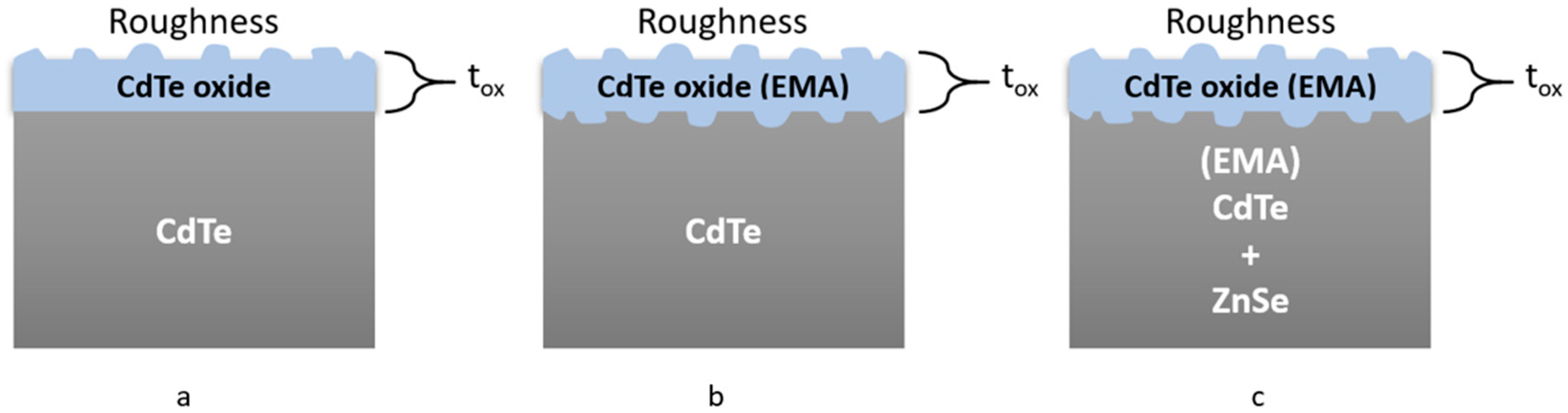
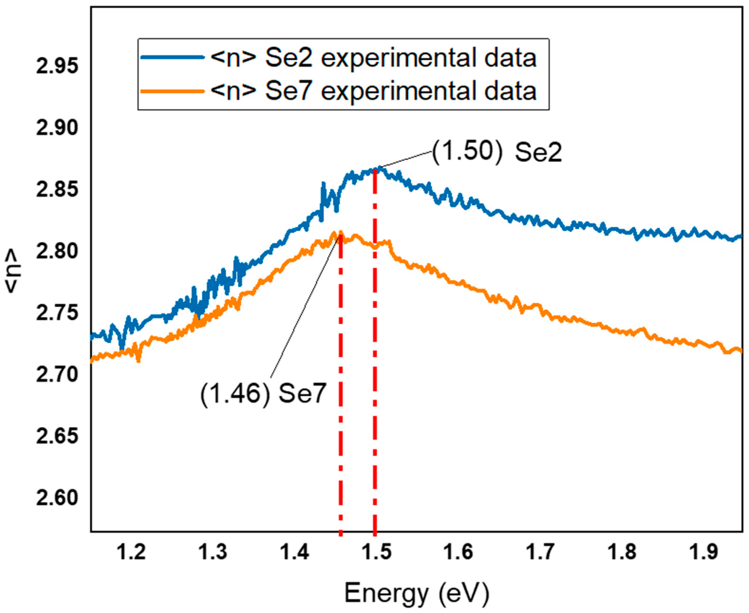
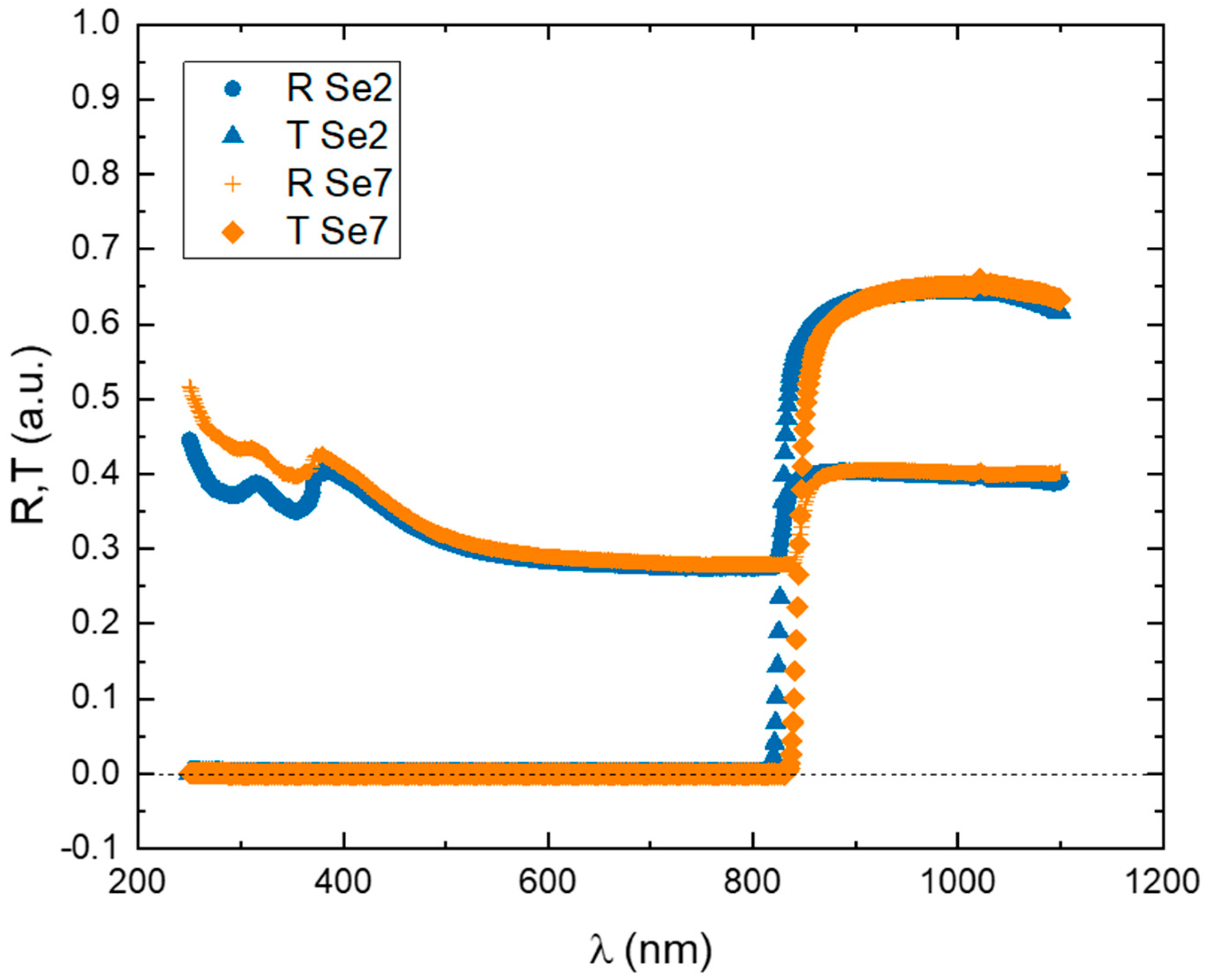
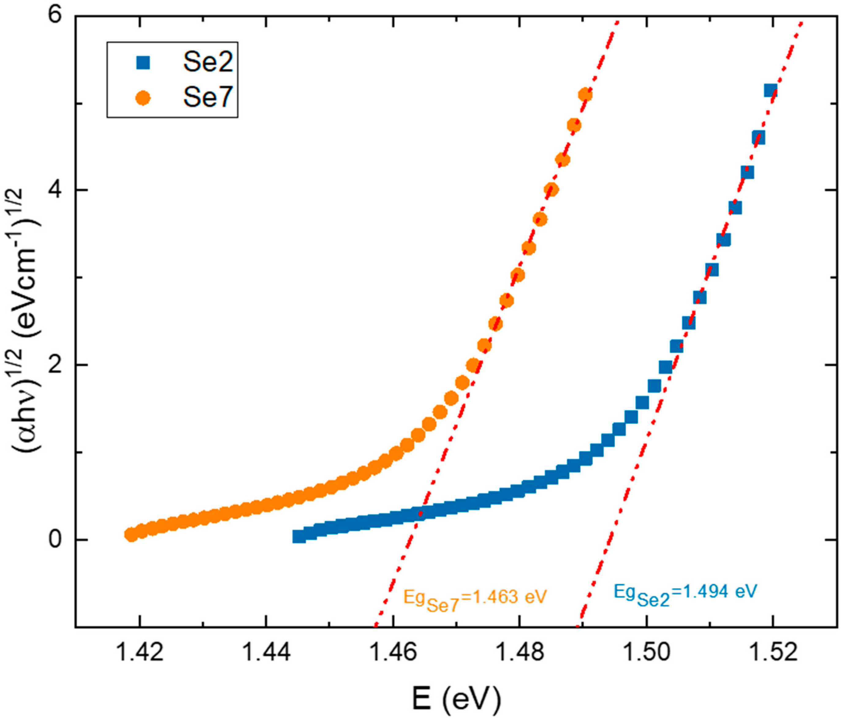
4. Results and Discussion
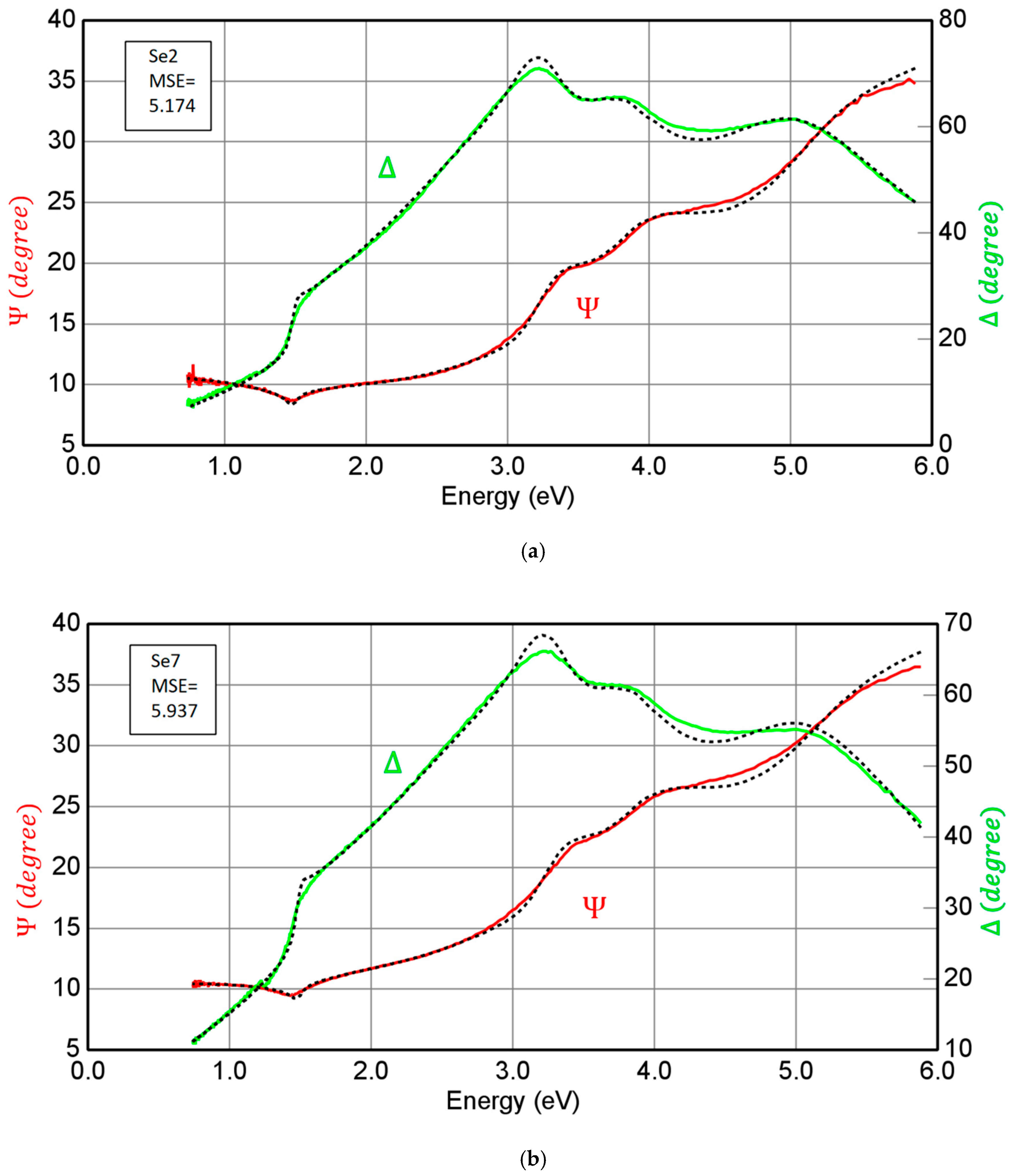
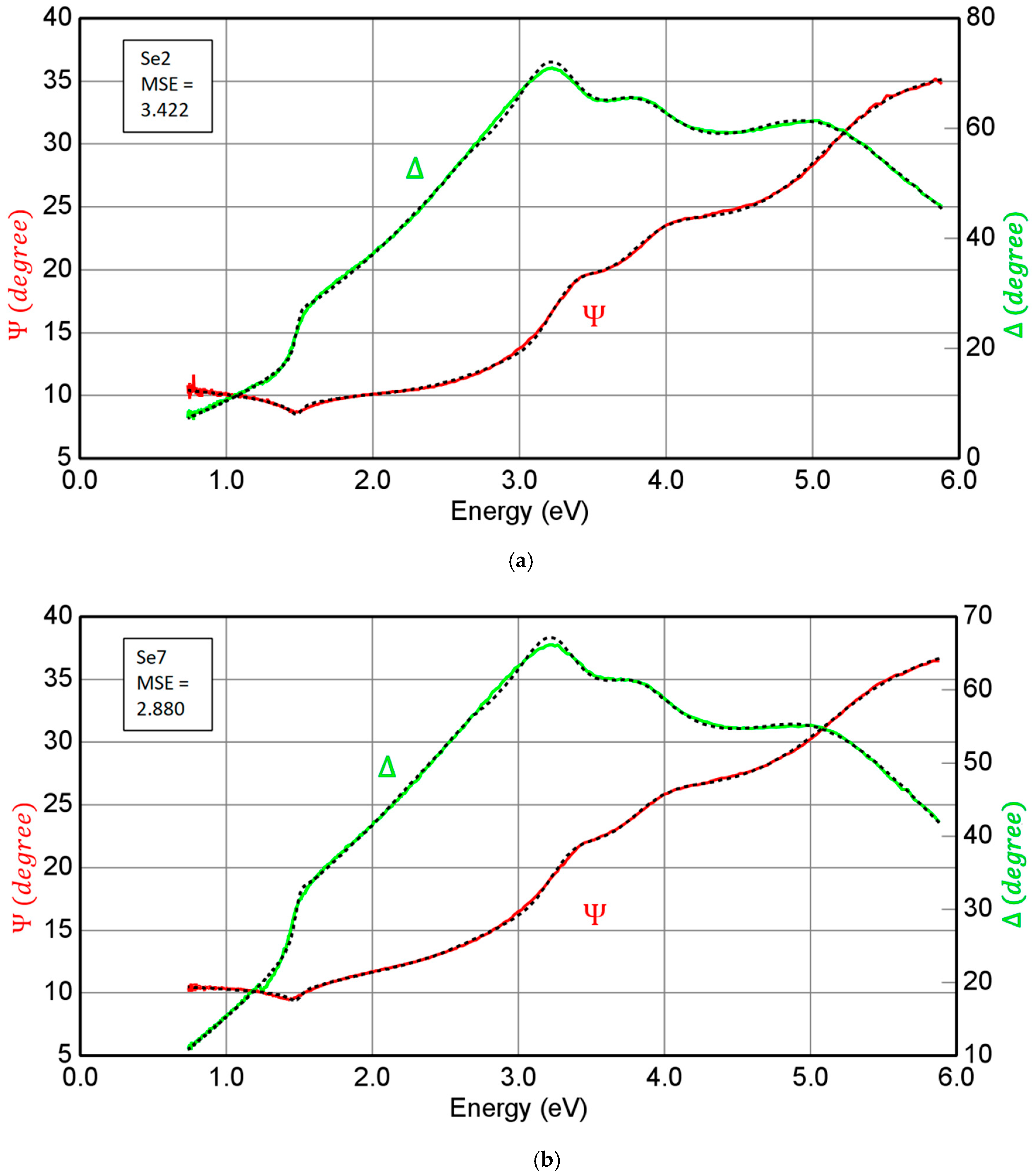
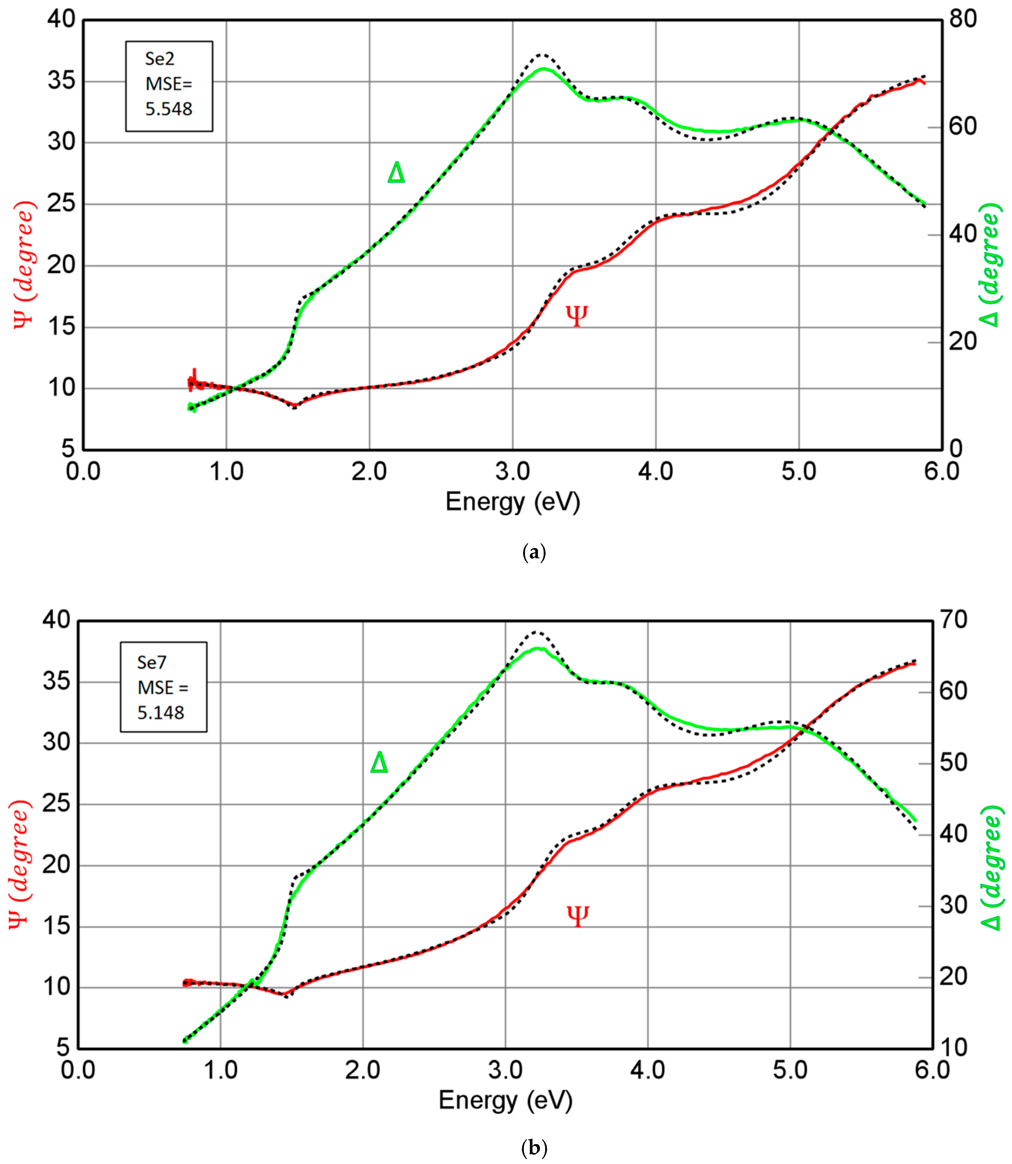
The study of the optical properties of a crystal provides a clear idea about its response to incident electromagnetic radiation at a particular frequency. This is important for selecting the proper material to be used for the fabrication of optoelectronic devices based on such optical features. In order to obtain the optical constants (n, K , and ε ) of the CZTS substrates covered by the surface oxide layer, a simple model assumption proposed by Yao et al. [15] was used as a first approximation. As the Zn and Se contents (x, y < 0.1) are much lower than those of Cd and Te, and we can approximate the CZTS oxide layer to that of the CdTe, covered with its corresponding surface oxide (the model sketched in Figure 1a), the optical parameters were predefined from the database of the CompleteEASE software. In this case, independent variables such as the oxide layer thickness and surface roughness were used during the fitting process. From the high MSE value that is shown in Figure 2a,b, the CZT model of Yao et al. was insufficient and incorrect for a complete ellipsometry investigation of our particular CZTS material, because our material was grown by VGF [6] not by epitaxial growth. Therefore, we also employed a more complete model development than the one proposed by Zázvorkata et al. [12]. This model involved a nonuniform surface substrate layer (CdTe), and an average value of material peaks and voids was included. As the Zn and Se contents (x, y < 0.1) are much lower than those of Cd and Te, we can approximate the CZTS oxide layer to that of CdTe. In addition, the peaks and voids result from the oxide layer growing on a rough nonuniform bulk CdTe surface. In turn, this oxide layer shows its surface roughness. This model is called the Effective Medium Approximation (EMA). An illustrative scheme is shown in Figure 1b. The EMA calculation is based on mixing the optical constants of two or three constituent materials to create a new composite material. The second model (Figure 1b) has two components: a CdTe substrate and a Bruggeman EMA layer consisting of an intermixing CdTe and CdTe oxide layer. In this case, there was a better correspondence between the theoretical model with a reduction in the oxide thickness layer (see Table 1 and Table 2). These oxide thicknesses were in the range of the ones reported by other authors [12,18]. Therefore, the mismatch may be due to an incorrect calculation in composition; so, an improved model is needed. In the third model (Figure 1c), we introduced Se and Zn as constituent elements of the substrate. The novelty of this model was to assume that the amount of Zn and Se was similar (x ~ y) in the material Cd1-xZnxTe1-ySey. Therefore, for all the binary compounds that constitute the quaternary compound CZTS, we maintained those that are in the same proportion.
C d 1 x Z n x T e 1 y S e y a · C d T e + b · Z n S e
where a and b represent the proportions in which the CdTe and ZnSe compounds are mixed to form Cd1-xZnxTe1-ySey. Considering the substrate material, an EMA model can mix the optical properties of the CdTe and ZnSe composites and an oxide layer formed with CdTe oxide and EMA CdTe-ZnSe. Consequently, the EMA inhomogeneity CdTe-ZnSe ratio (a, b) model allows the determination of the compound composition and the comparison with our previous work with X-ray diffraction results [6]. Finally, the model and experimentally measured values shown in Figure 3 overlap, thus demonstrating a great fit compared to the most rudimentary models Figure 2 and Figure 4. The higher the selenium content, the better the match (see the exact values in Table 1 and Table 2). The thickness and roughness of the oxide layer in both cases showed similar values as expected because the samples underwent the same polishing treatments. The different oxide coefficients of the Cauchy equations [17] are tabulated in Table 3. The percentages in Table 4 show that the ellipsometry gave us the composition of the samples resulting in 12.9% of ZnSe (ratio b) for the sample Se2. If we add both nominal percentages of Zn and Se, the result would be 12%, which is very close to the value obtained by the X-ray diffraction in [6]. In turn, it is similar for the composition Se7, where the value calculated by the EMA was 18.2% (ratio b), while the composition would be 17%.
Table 1. Ellipsometry fit parameters obtained for the sample Se2 with the different models proposed in Figure 1.
Se2Teox (Å)Roughness (Å)MSE
Model 128 ± 3 A93 ± 45.174
Model 218 ± 1 A76 ± 35.548
Model 321 ± 1 A84 ± 43.422
Table 2. Ellipsometry fit parameters obtained for the sample Se7 with the different models proposed in Figure 1.
Se7Teox (Å)Roughness (Å)MSE
Model 154 ± 6 A139 ± 25.937
Model 227 ± 1 A 114 ± 45.148
Model 331 ± 3 A126 ± 62.880
Figure 1. Model structures for fitting the ellipsometry experimental data. (a) Simple model with a flat interface between the substrate and oxide layer and with surface roughness, (b) EMA structure model with the CdTe substrate and CdTe oxide with surface roughness, (c) double EMA model with EMA as a substrate of CdTe and ZnTe and the substrate EMA and oxide CdTe with surface roughness. In all the models, the substrate is a semi-infinite layer, and the thickness of the oxide layer is denoted by tox.
Crystals 13 00693 g001
Figure 2. Evolution of the ellipsometric parameters Ψ and Δ and the fit to the ellipsometry model 1 proposed in Figure 1a for different selenium compositions (a) Se2 and (b) Se7. The lines represented by different colours are the experimental data, and the dashed lines correspond to the model.
Crystals 13 00693 g002
The dispersion curves in Figure 5 indicate a sharp increase at shorter wavelengths corresponding to the fundamental absorption of energy across the bandgap [19]. The bandgap energy shifted to lower energies with the addition of Se to the CZTS compound, as shown in Figure 5. This result agreed with the complete structural and optoelectronic CZTS theoretical model by Chanda et al. [20]. Recently, several authors had similar bandgap values using other characterisation techniques, around 1.468–1.56 eV for composition (x = 0.1 and y = 0.002) and 1.54–1.56 eV for composition (x = 0.1 and y = 0.007) [7,21,22,23,24,25]. Moreover, that decrease in bandgap followed the well-known Vergard’s Law proposed by Brill et al. [23]. These results agreed with our previous research, showing that the VGF method generates reproducible CZTS crystals with a zinc blend crystal structure, in which the selenium addition causes a reduction in the lattice parameter and compositional/lattice disorder [6,26]. Much effort has been recently made to analyse CZTS’s compositional and spectroscopic properties. However, to the best of our knowledge, this is the first time that experimental measurements of both the composition and bandgap have been performed on this material. This kind of analysis is essential to characterise the ideal composition to ensure the correct charge collection and to obtain gamma sensitivity in radiation detectors [27].
Finally, a typical transmittance and reflectance spectrum for the studied sample is shown in Figure 6. The optical bandgap was estimated using the absorption coefficient α [28] and applying the Tauc equation [24,29]:
α h ν = A ( h ν E G ) β ,
where α h ν is the photon energy, A is a constant, E G is the optical bandgap, and β is a parameter that depends on the type of transition (e.g., whether it is a direct or indirect transition). For CZTS, n is 0.5 because it is a direct bandgap semiconductor. Therefore, a plot of ( α h ν )1/2 against energy provided a straight line, as shown in Figure 7, whose intercept with the energy axis gave the energy of the allowed direct Valence Band (VB) to Conduction Band (CB) transition. This bandgap value was in excellent agreement with the E G values obtained by ellipsometry (see Figure 5).

5. Conclusions

The optical properties of the Cd1-xZnxTe1-ySey quaternary compound for different selenium contents (y = 0.02 (Se2) and 0.07 (Se7)) were determined for the first time by using the nondestructive ellipsometry technique. Three different models to analyse the experimental data were proposed, with the most accurate including the binary compound ZnSe mixing the optical properties with the Effective Medium Approximation (EMA) with the compound CdTe and its associated oxide.
The absorption energy of the real part of the absorption coefficient gives the material bandgap, which has been shown to decrease with an increasing selenium concentration, as theoretically predicted by Vegard’s Law. The bandgap value calculated based on the absorption coefficient agreed significantly with the gap values obtained by the ellipsometry.
The EMA mixing percentages of the ZnSe compound in the CdTe were 12.9% for the sample Se2 (Cd0.9Zn0.1Te0.98Se0.02) and 18.9% for the sample Se7 (Cd0.9Zn0.1Te0.93Se0.07). These values are very close to the nominal 12% and 17% values obtained by X-ray diffraction in our previous work [6]. Therefore, the present work proposes the ellipsometry technique as a fundamental tool for the acquisition of the compositional data, optical properties, surface roughness, and surface oxide thickness of CdTe.
Finally, the relevance of this work is proposing ellipsometry as another method to determine the composition of the CZTS material, allowing it to be a reality in the market to generate competitive, high-resolution, and low-cost X-ray and gamma radiation detectors.

Author Contributions

Conceptualization, A.F.B.d.C. and L.M.H.; methodology, A.F.B.d.C., J.L.P.C.-a. and L.M.H.; sample preparation, J.L.P.C.-a. and L.M.H.; formal analysis, L.M.H.; validation, A.F.B.d.C., and J.L.P.C.-a.; investigation, A.F.B.d.C., J.L.P.C.-a. and L.M.H.; writing—original draft preparation L.M.H.; writing—review and editing, A.F.B.d.C., J.L.P.C.-a. and L.M.H.; resources, J.L.P.C.-a. and A.F.B.d.C.; project administration, J.L.P.C.-a. All authors have read and agreed to the published version of the manuscript.

Funding

This research received no external funding.

Data Availability Statement

The data presented in this study are available on request from the corresponding author.

Acknowledgments

This paper is indebted to Andrés Redondo for his advice on ellipsometry measurements.

Conflicts of Interest

The authors declare no conflict of interest.

References

  1. Martinez-Herraiz, L.; Ruiz, E.; Brana, A.F.; Plaza, J. Effects of Surface Treatments on the Performance of CdZnTeSe Radiation Detectors. In Proceedings of the 2021 13th Spanish Conference on Electron Devices (CDE), Sevilla, Spain, 9–11 June 2021; pp. 33–36. [Google Scholar] [CrossRef]
  2. Talwar, D.N.; Becla, P.; Lin, H.-H.; Feng, Z.C. Assessment of intrinsic and doped defects in Bridgman grown Cd1−xZnxTe alloys. Mater. Sci. Eng. B 2021, 269, 115160. [Google Scholar] [CrossRef]
  3. Kleppinger, J.W.; Chaudhuri, S.K.; Roy, U.N.; James, R.B.; Mandal, K.C. Growth of Cd0.9 Zn0.1Te1−ySey Single Crystals for Room Temperature Gamma-Ray Detection. IEEE Trans. Nucl. Sci. 2021, 2429–2434. [Google Scholar] [CrossRef]
  4. Roy, U.; Camarda, G.; Cui, Y.; James, R. Advances in CdZnTeSe for Radiation Detector Applications. Radiation 2021, 1, 123–130. [Google Scholar] [CrossRef]
  5. Roy, U.N.; Camarda, G.S.; Cui, Y.; Yang, G.; James, R.B. Impact of selenium addition to the cadmium-zinc-telluride matrix for producing high energy resolution X-and gamma-ray detectors. Sci. Rep. 2021, 11, 1–10. [Google Scholar] [CrossRef] [PubMed]
  6. Martínez-Herraiz, L.; Braña, A.; Plaza, J. Vertical Gradient Freeze Growth of two inches Cd1−x ZnxTe1−y Sey ingots with different Se content. J. Cryst. Growth 2021, 573, 126291. [Google Scholar] [CrossRef]
  7. Roy, U.N.; Camarda, G.S.; Cui, Y.; Gul, R.; Yang, G.; Zazvorka, J.; Dedic, V.; Franc, J.; James, R.B. Evaluation of CdZnTeSe as a high-quality gamma-ray spectroscopic material with better compositional homogeneity and reduced defects. Sci. Rep. 2019, 9, 1–7. [Google Scholar] [CrossRef]
  8. Gul, R.; Roy, U.N.; Camarda, G.S.; Hossain, A.; Yang, G.; Vanier, P.; James, R.B. A comparison of point defects in Cd1−xZnxTe1−ySey crystals grown by Bridgman and traveling heater methods. J. Appl. Phys. 2017, 121, 125705. [Google Scholar] [CrossRef]
  9. Moravec, P.; Franc, J.; Dědič, V.; Minárik, P.; Elhadidy, H.; Šíma, V.; Grill, R.; Roy, U. Microhardness study of CdZnTeSe crystals for X-ray and gamma ray radiation detectors. In Proceedings of the 2019 IEEE Nuclear Science Symposium and Medical Imaging Conference (NSS/MIC), Manchester, UK, 26 October–2 November 2019; pp. 1–4. [Google Scholar]
  10. Mycielski, A.; Burger, A.; Sowinska, M.; Groza, M.; Szadkowski, A.; Wojnar, P.; Siffert, P. Is the (Cd, Mn) Te crystal a prospective material for X-ray and γ-ray detectors? Phys. Status Solidi (C) 2005, 2, 1578–1585. [Google Scholar] [CrossRef]
  11. Chaudhuri, S.K.; Sajjad, M.; Mandal, K.C. Pulse-shape analysis in Cd0.9Zn0.1Te0.98Se0.02 room-temperature radiation detectors. Appl. Phys. Lett. 2020, 116, 162107. [Google Scholar] [CrossRef]
  12. Zázvorka, J.; Franc, J.; Beran, L.; Moravec, P.; Pekárek, J.; Veis, M. Dynamics of native oxide growth on CdTe and CdZnTe X-ray and gamma-ray detectors. Sci. Technol. Adv. Mater. 2016, 17, 792–798. [Google Scholar] [CrossRef]
  13. Zázvorka, J.; Franc, J.; Statelov, M.; Pekárek, J.; Veis, M.; Moravec, P.; Mašek, K. Optical and electrical study of CdZnTe surfaces passivated by KOH and NH4F solutions. Appl. Surf. Sci. 2016, 389, 1214–1219. [Google Scholar] [CrossRef]
  14. Agbalagba, E.O.; Drabo, M.L.; Egarievwe, S.U.; Roy, U.N.; Davis, A.H.; Israel, M.B.; Alexander, P.L.; James, R.B. Characterization of CdZnTeSe Nuclear Detector Chemically Etched in Bromine Methanol. Mater. Sci. Appl. 2021, 12, 363–373. [Google Scholar] [CrossRef]
  15. Yao, H.W.; Erickson, J.C.; Barber, H.B.; James, R.B.; Hermon, H. Optical properties of Cd0.9Zn0.1 Te studied by variable angle spectroscopic ellipsometry between 0.75 and 6.24 eV. J. Electron. Mater. 1999, 28, 760–765. [Google Scholar] [CrossRef]
  16. Fujiwara, H.; Collins, R.W. (Eds.) Spectroscopic Ellipsometry for Photovoltaics: Volume 1: Fundamental Principles and Solar Cell Characterization; Springer Series in Optical Sciences; Springer International Publishing: Cham, Switzerland, 2018; Volume 212, ISBN 978-3-319-75375-1. [Google Scholar]
  17. Hilfiker, N.J.; Tiwald, T. Dielectric function modeling. In Spectroscopic Ellipsometry for Photovoltaics. Volume 1: Fundamental Principles and Solar Cell Characterization; Fujiwara, H., Collins Robert, W., Eds.; Springer Nature: Cham, Switzerland, 2018; pp. 115–153, Chapter 5. [Google Scholar]
  18. Badano, G.; Million, A.; Canava, B.; Tran-Van, P.; Etcheberry, A. Fast Detection of Precipitates and Oxides on CdZnTe Surfaces by Spectroscopic Ellipsometry. J. Electron. Mater. 2007, 36, 1077–1084. [Google Scholar] [CrossRef]
  19. Batra, V.; Kotru, S.; Varagas, M.; Ramana, C.V. Optical constants and band gap determination of Pb0.95La0.05Zr0.54Ti0.46O3 thin films using spectroscopic ellipsometry and UV–visible spectroscopy. Opt. Mater. 2015, 49, 123–128. [Google Scholar] [CrossRef]
  20. Chanda, S.; Ghosh, D.; Debnath, B.; Debbarma, M.; Bhattacharjee, R.; Chattopadhyaya, S. Calculations of the structural and optoelectronic properties of cubic Cd x Zn 1− x Se y Te 1− y semiconductor quaternary alloys using the DFT-based FP-LAPW approach. J. Comput. Electron. 2020, 19, 1–25. [Google Scholar] [CrossRef]
  21. Roy, U.N.; Camarda, G.S.; Cui, Y.; Gul, R.; Hossain, A.; Yang, G.; Zazvorka, J.; Dedic, V.; Franc, J.; James, R.B. Role of selenium addition to CdZnTe matrix for room-temperature radiation detector applications. Sci. Rep. 2019, 9, 1–7. [Google Scholar] [CrossRef]
  22. Roy, U.N.; Camarda, G.S.; Cui, Y.; James, R.B. Optimization of selenium in CdZnTeSe quaternary compound for radiation detector applications. Appl. Phys. Lett. 2021, 118, 152101. [Google Scholar] [CrossRef]
  23. Brill, G.; Chen, Y.; Amirtharaj, P.M.; Sarney, W.; Chandler-Horowitz, D.; Dhar, N.K. Molecular beam epitaxial growth and characterization of Cd-based II–VI wide-bandgap compounds on Si substrates. J. Electron. Mater. 2005, 34, 655–661. [Google Scholar] [CrossRef]
  24. Hwang, S.; Yu, H.; Bolotnikov, A.E.; James, R.B.; Kim, K. Anomalous Te Inclusion Size and Distribution in CdZnTeSe. IEEE Trans. Nucl. Sci. 2019, 66, 2329–2332. [Google Scholar] [CrossRef]
  25. Nag, R.; Chaudhuri, S.K.; Kleppinger, J.W.; Karadavut, O.; Mandal, K.C. Characterization of vertical Bridgman grown Cd0.9Zn0.1Te0.97Se0.03 single crystal for room-temperature radiation detection. J. Mater. Sci. Mater. Electron. 2021, 32, 26740–26749. [Google Scholar] [CrossRef]
  26. Roy, U.N.; Baker, J.N.; Camarda, G.S.; Cui, Y.; Yang, G.; James, R.B. Evaluation of crystalline quality of traveling heater method (THM) grown Cd0.9Zn0.1Te0.98Se0.02 crystals. Appl. Phys. Lett. 2022, 120, 242103. [Google Scholar] [CrossRef]
  27. Chaudhuri, S.K.; Kleppinger, J.W.; Karadavut, O.; Nag, R.; Mandal, K.C. Quaternary Semiconductor Cd1−xZnxTe1−ySey for High-Resolution, Room-Temperature Gamma-Ray Detection. Crystals 2021, 11, 827. [Google Scholar] [CrossRef]
  28. Nichelatti, E. Complex refractive index of a slab from reflectance and transmittance: Analytical solution. J. Opt. A Pure Appl. Opt. 2002, 4, 400–403. [Google Scholar] [CrossRef]
  29. Rakhshani, A.E. Electrodeposited CdTe—Optical properties. J. Appl. Phys. 1997, 81, 7988–7993. [Google Scholar] [CrossRef]
Figure 3. Evolution of the ellipsometric parameters Ψ and Δ and the fit to the ellipsometry model 3 proposed in Figure 1c for different selenium compositions (a) Se2 and (b) Se7. The lines represented by different colours are the experimental data, and the dashed lines correspond to the model.
Crystals 13 00693 g003
Figure 4. Evolution of the ellipsometric parameters Ψ and Δ and the fit to the ellipsometry model 2 proposed in Figure 1b for different selenium compositions (a) Se2 and (b) Se7. The lines represented by different colours are the experimental data, and the dashed lines correspond to the model.
Crystals 13 00693 g004
Figure 5. The energy dependence of the optical refractive index n and the calculation of its associated bandgap for samples at different concentrations of selenium, Se2 and Se7.
Crystals 13 00693 g005
Figure 6. The transmittance and reflectance of the samples at different concentrations of selenium (Se2 and Se7).
Crystals 13 00693 g006
Figure 7. ( α h ν )1/2 versus energy of the Se2 and Se7 samples at room-temperature measurement. The intercept with the energy axis corresponds to the optical bandgap of CZTS.
Crystals 13 00693 g007
Table 3. The CdTe-ox parameter used in the Cauchy equations (see reference [17]).
SampleABCExponent
Se25.7 ± 0.6−0.30 ± 0.080.011 ± 0.0030.6 ± 0.1
Se74.6 ± 0.4−0.17 ± 0.040.006 ± 0.0020.4 ± 0.1
Table 4. The EMA analysis composition of model 3.
SampleCdTe % (a Ratio)ZnSe % (b Ratio)
Se287.112.9
Se781.818.2
Disclaimer/Publisher’s Note: The statements, opinions and data contained in all publications are solely those of the individual author(s) and contributor(s) and not of MDPI and/or the editor(s). MDPI and/or the editor(s) disclaim responsibility for any injury to people or property resulting from any ideas, methods, instructions or products referred to in the content.

