1. Introduction
Traditional pressure sensors are usually operated based on mechanical elastic deformation [
1,
2], the piezoelectric effect [
3,
4,
5], or the resistance–strain effect of materials [
6,
7]. The disadvantages of these kinds of sensors are that the response is hysteretic, the sensitivity coefficient is greatly affected by the environment temperature, and the measuring accuracy is not high enough. Especially in the cryogenic environment, the physical properties of materials fundamentally change, which greatly exceeds the working range of conventional pressure sensors. Therefore, it is necessary to develop revolutionary structures and materials to manufacture pressure sensors with high sensitivity and stability in low-temperature surroundings.
Periodic one-dimensional photonic crystals can be formed by alternating arrangement of two dielectric materials with different refractive indices [
8]. Photonic crystals can support photonic bandgaps in which light waves cannot transmit through the systems [
9,
10]. However, if a defect is introduced into the periodic structure to form a defective photonic crystal, a defect mode arises in the center of the bandgap [
11,
12]. The defective resonance mode allows the light energy to pass through the photonic crystal without reflection. The defect mode may strongly localize the electric field and is often used in the study of optical bistability [
13,
14,
15], laser points [
16,
17], exceptional points [
18], and temperature sensors [
19]. The central wavelength of the defect mode is governed by the refractive index of defect. Therefore, the central wavelength of defect mode can be regulated by external parameters [
20].
Superconductors and semiconductors, which refractive indices depend on for the environment temperature and the external stationary pressure, have also been utilized for photonic crystals [
21,
22]. A superconducting material is embedded in the photonic crystal to form a defect and the defective resonance mode is sensitive to the surroundings under the critical temperature of the superconductor [
23,
24]. Segovia-Chaves, F., et al. discussed the shifting of transmission spectra and the photonic bandgap appearance in superconductor–semiconductor periodic photonic crystals [
25]. Increasing the temperature and incident angle, the transmission spectrum moves to the lower-frequency direction, and meanwhile, the bandwidth of the photonic bandgap increases. Furthermore, they also showed that the transmission spectrum shifts to higher frequency values, and new bandgaps appear by changing the hydrostatic pressure.
Sabra, W., et al. investigated reflection spectra of light waves in defect photonic crystals composed of superconductor Hg-1223 and semiconductor GaAs with a substrate [
21]. The operating wavelength is local in the mid-IR region. It showed that the highest pressure sensitivity is 1.7467 nm/GPa at the hydrostatic pressure of 6 GPa. It is well known that the defect photonic crystal can support a defect mode, which is a transmission mode, with high transmittance and low reflectance. Since the defect mode strongly depends on the hydrostatic pressure applied on the superconducting photonic crystal, obviously, the phenomenon is more convenient and evident through probing the transmitted beam of defect mode than by detecting the reflected beam.
A scheme is needed to induce the hydrostatic pressure and the transmitted beam, for which we added two optical trapezoid waveguides on both sides of the defective photonic crystal. Therefore, it is meaningful to construct defective photonic crystals with superconducting and semiconducting materials and subsequently apply the pressure on the structures to realize high-sensitivity and linearity sensors in the extremely low-temperature environment.
Superconductor and semiconductor slabs are laid along the X-axis to form a one-dimensional photonic crystal. The photonic crystal is periodic, and a defect is local at the center of the system. The bandgap and the defect resonant mode of the photonic crystal are investigated and the dependence of the defect mode on the applied pressure intensity is explored as well. We subsequently study the sensitivity coefficient of pressure sensors and the influence of the environment temperature. The resonance and wavelength selectivity of defect mode are then discussed through improving the periodic number of structures. Furthermore, regulation of the defect mode by changing the incident angle is demonstrated as well. This investigation has an application in cryogenic pressure-optic sensors.
2. Superconducting Photonic Crystals
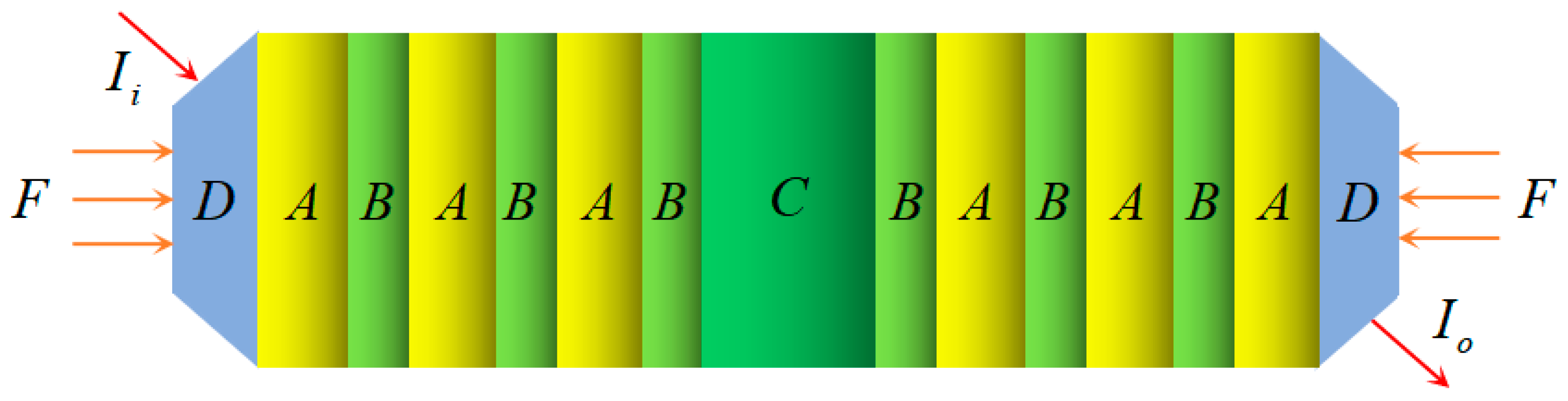
The system is composed by superconductor and semiconductor materials as shown in
Figure 1. The structure can be denoted by ABABABCBABABA, where A and C are superconductor slabs. The symbol of B represents the semiconductor slab. Obviously, this system is viewed as a one-dimensional defective photonic crystal and can be expressed as (AB)
NC(BA)
N, where
N = 3 is the periodic number of the photonic crystal and C is the defect of the periodic photonic crystal. The periodic number can also be set as other positive integers.
The thickness of slab A is set as a quarter of optical wavelength, i.e., da0 = λ0/(4na0), where na0 is the refractive index of A with the incident wavelength of λ0. The central wavelength is λ0 = 1.55 μm. The corresponding thickness of slab B is also equal to the 1/4 optical wavelength db0 = λ0/(4nb0), where nb0 is the refractive index of B with the same wavelength λ0. The defect thickness is dc0 = λ0/(2nc0) and nc0 is the refractive index of C. The slab has an optical wavelength thickness twice as much as the value of A and B, so the component of C is treated as a defect in comparison with periodic photonic crystals. The whole structure is symmetric to the center.
The symbols Ii and Io represent the incident light beam and the transmitted light beam, respectively. The two letter Ds at the inputting and outputting ports are coupled wave guides. The symbol of F expresses the stationary pressure. Therefore, the guides of Ds play the parts of transferring pressure and coupling optical waves simultaneously. The profile of optical wave guide D is an isosceles trapezoid with a base angle of 45°. The incident light beam perpendicularly impinges on the waist of D.
We only give a base angle value of 45 degrees for the waveguide cross profile in the schematic diagram to demonstrate the operating principle. In other cases, one can adjust the base angle of the trapezoid of the cross profile to satisfy the requirement of normal incidence referring to the waist face of the trapezoid waveguide.
The superconductor HgBa
2Ca
2Cu
3O
8+δ is chosen for slabs A and C. Slab B is set as semiconductor material GaAs. The superconducting material of HgBa
2Ca
2Cu
3O
8+δ is lossless under certain temperatures. The permittivity of HgBa
2Ca
2Cu
3O
8+δ is governed by
where
c is the speed of light in free space,
ω = 2π
c/λ is the angular frequency of light wave, and
λ is the incident wavelength [
26]. London penetration depth is given by
where the parameter
Te is circumstance temperature,
Tc is the critical temperature and is expressed as
Te = A
1 + B
1P + D
1P2, and
P is the stationary intensity of pressure. The other parameters are set as A
1 = 134, B
1 = 2.009, and D
1 = −4.194 × 10
−2 [
24].
The material of slab B is set as GaAs and the permittivity of this semiconductor is
where
K is Kelvin temperature [
27]. The thickness of slab B is a function of
P, and the relation can be expressed by
where
db0 is the initial thickness of B for
P = 0 GPa and the elastic constants are
S11 = 1.16 × 10
−2 GPa
−1 and
S12 = −3.7 × 10
−3 GPa
−1, respectively [
27].
The refractive index of superconductor HgBa2Ca2Cu3O8+δ is na0 = 0.9984 for the environment temperature Te = 100 K and intensity of pressure P = 100 GPa. The refractive index of GaAs is nb0 = 3.2773 with the same condition. The thicknesses of A and B are da0 = λ0/(4na0) = 0.3881 μm and db0 = λ0/(4nb0) = 0.3881 μm, respectively. The thickness of C is two times that of A and the value is dc0 = λ0/(2nc0) = 0.7762 μm. Silicon dioxide (SiO2) can be utilized for optical waveguide and its refractive index is given with a fixed value nd = 1.5 for simplicity in simulations.
The superconducting material of HgBa
2Ca
2Cu
3O
8+δ has been used for polychromatic filters in semiconductor–superconductor dielectric periodic and quasi-periodic hybrid photonic crystals, and the transmission peaks could be tuned by temperature in a cryogenic environment [
28]. One also regulates the photonic bandgap and transmittance by the value of environment temperature in superconducting Octonacci photonic crystals composed of HgBa
2Ca
2Cu
3O
8+δ [
29].
3. Defect Mode Dependence and Pressure Sensing
For a transverse magnetic wave incident in the structure, the transmission and reflection characteristics of light can be simulated by the transmission matrix method (TMM) [
30].
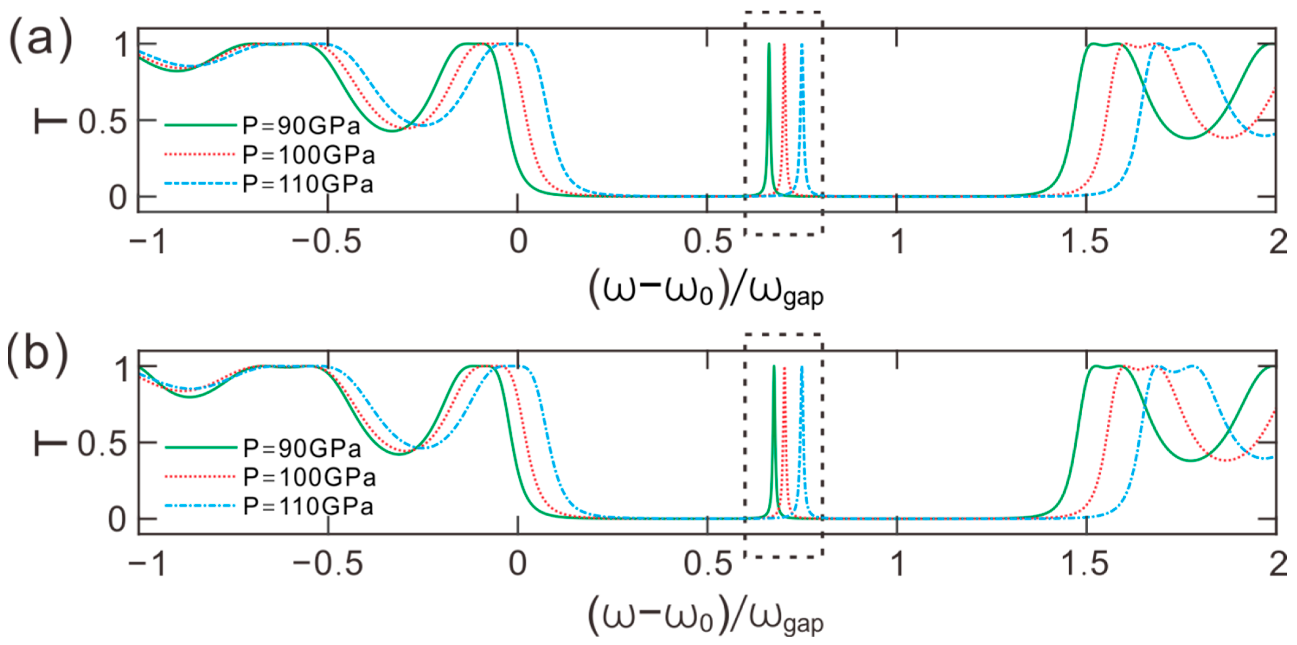
Figure 2a gives the transmission spectra under different values of pressure intensity. The environment temperature is
Te = 50 K. The vertical coordinate
T represents transmittance and the horizontal axis is denoted by the normalized frequency (
ω –
ω0)/
ωgap, where the bandgap of the photonic crystal is
ωgap = 4
ω0arcsin│(n
a0 − n
b0)/(n
a0 + n
b0)│
2/π. The symbols
ω = 2π
c/
λ and
ω0 = 2π
c/
λ0 mean angular frequency of incident light and central angular frequency, respectively. The parameter c is the speed of light in the vacuum.
One can see that there are three transmission spectra for three given values of pressure intensity: P = 90, 100, and 110 GPa. A bandgap exists in each spectrum and a transmission mode arises in the center of the bandgap, denoted by a dotted box. The transmission peak moves to the right as the intensity of pressure increases, viz., the central wavelength decreases with the increase in the pressure intensity. The corresponding central wavelengths of defect modes are orderly: λp = 1.0508, 1.0307, and 1.0084 μm for P = 90, 100, and 110 GPa. The wavelength interval between the corresponding peaks for P = 90 and 110 GPa is 0.0424 μm.
The designed structure is a photonic crystal with a defect. The defect can localize the electric field, which approves a transmission mode, i.e., the defect mode. The whole system is viewed as a resonant cavity. The defect is equal to the cavity body and the left and right periodic dielectric multilayers equate to two reflectors. Light waves propagate forward in dielectrics and are reflected backward by the reflectors. Consequently, a resonant mode is achieved.
It can be seen that the central wavelength of defect mode is different with different stationary pressure, that is, there is a one-to-one correspondence between the central wavelength of defect mode and the static pressure. Therefore, the stationary pressure on the defective photonic crystal can be detected by the central wavelength of transmission mode.
Figure 2b provides the transmission spectra for different pressure intensity as the environment temperature is
Te = 100 K. The photonic bandgap and defect mode are also induced by changing the light frequency. The central wavelengths of defect modes are
λp = 1.0448, 1.031, and 1.0091 μm for
P = 90, 100, and 110 GPa, in order. The difference in resonant wavelengths between the two corresponding peaks for
P = 90 and 110 GPa is 0.0357 μm. Compared with the results in the case of
Te = 50 K, the interval of frequency between two adjacent peaks becomes narrower for
Te = 100 K. Therefore, the defect mode can be controlled by the environment temperature as well.
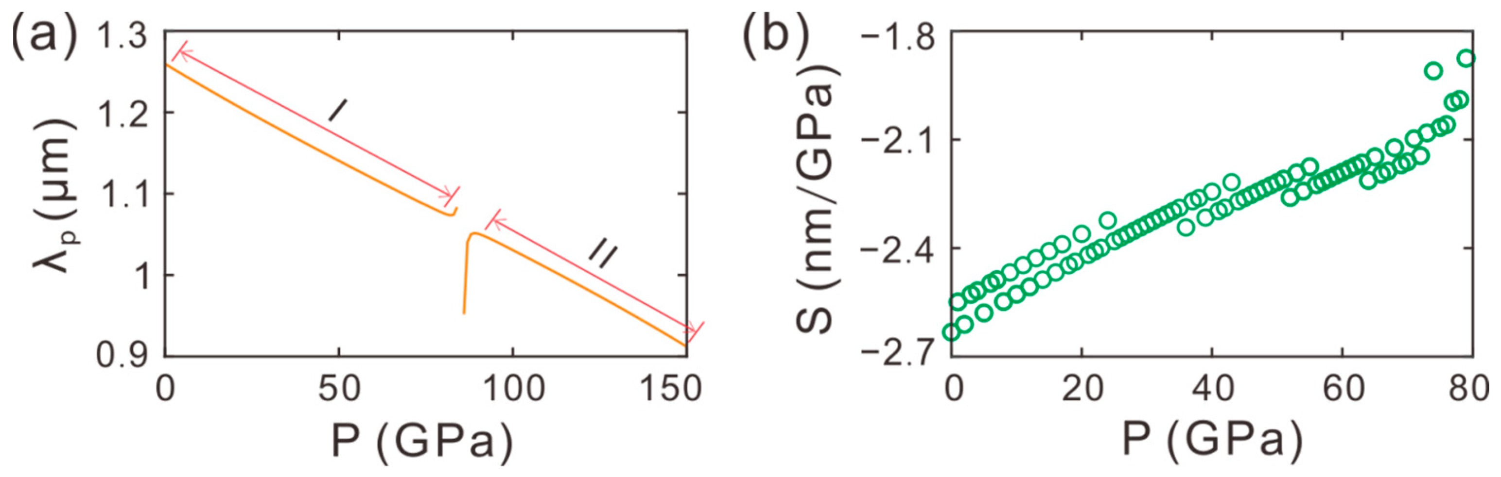
The central wavelength of the defect mode is denoted by
λp, and the environment temperature is set as
Te = 50 K.
Figure 3a gives
λp changing with the external stationary pressure intensity
P. The incident angle is set as 45°. It shows that the value of
λp decreases roughly with the increase in
P. There are two nearly linear sections I and II in the dependent relationship between
λp and
P. The defect mode cannot be observed at the value of
P = 85 GPa. Consequently, there is an abnormal gap in the relationship curve around
P = 85 GPa. The optical loss of superconductor HgBa
2Ca
2Cu
3O
8+δ is so great at the value of pressure intensity 85 GPa that the optical energy of the central defect mode has been dissipated entirely. In the stationary pressure probing, it requires the input–output relationship curve to be linear, so section I or II can be selected as the working region of sensors in practical applications.
At the temperature of
Te = 50 K, section I is chosen for the working region, as the defect photonic crystal is utilized for pressure sensing.
Figure 3b provides the sensitivity coefficient of pressure sensors. The stationary pressure intensity varies in the range of [0 GPa, 80 GPa]. It can be seen that the sensitivity coefficient is negative, and the absolute value of sensitivity coefficient decreases mildly as the pressure intensity increases. The sensitivity coefficient of sensors is |
S| = 1.9 nm/GPa at the pressure intensity
P = 80 GPa.
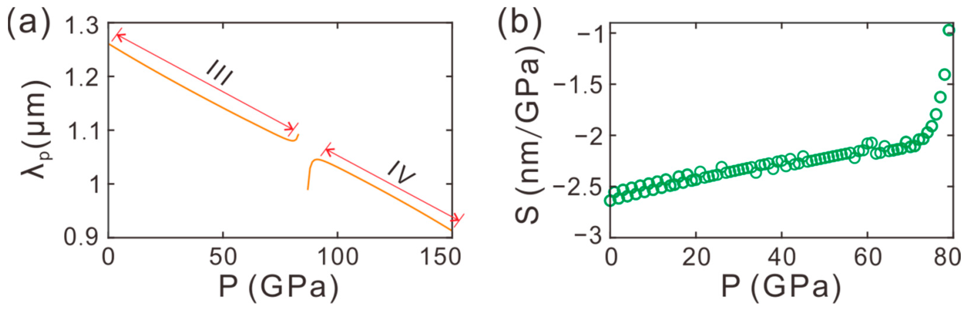
Increasing the environment temperature to
Te = 100 K,
Figure 4a gives the central wavelength of the defect mode changing with the stationary pressure intensity. The incident angle is set as 45° as well. Similarly, it can be found that the value of
λp decreases as the parameter
P increases. Two nearly linear working regions III and IV exist in the whole change relation curve. The defect mode disappears in the interval
P = [84 GPa, 87 GPa], which contributed to the giant loss of HgBa
2Ca
2Cu
3O
8+δ in this pressure section. One can choose sections III and IV to utilize for the operating range of sensors.
One can choose section III for the working region to probe the stationary pressure intensity at the temperature of
Te = 100 K.
Figure 4b gives the sensitivity coefficient of sensors as the stationary pressure intensity changes. The variation range is set as the section of [0 GPa, 80 GPa]. The horizontal axis is the inputting stationary pressure. The absolute value |
S| also slightly varies as the pressure intensity increases. The sensitivity coefficient of sensors is |
S| = 0.97 nm/GPa at the pressure intensity
P = 80 GPa. Therefore, the sensitivity at
Te = 100 K is generally lower than that at
Te = 50 K. The sensitivity coefficient can be kept constant by mathematical means such as linear fitting, such as the least square method.
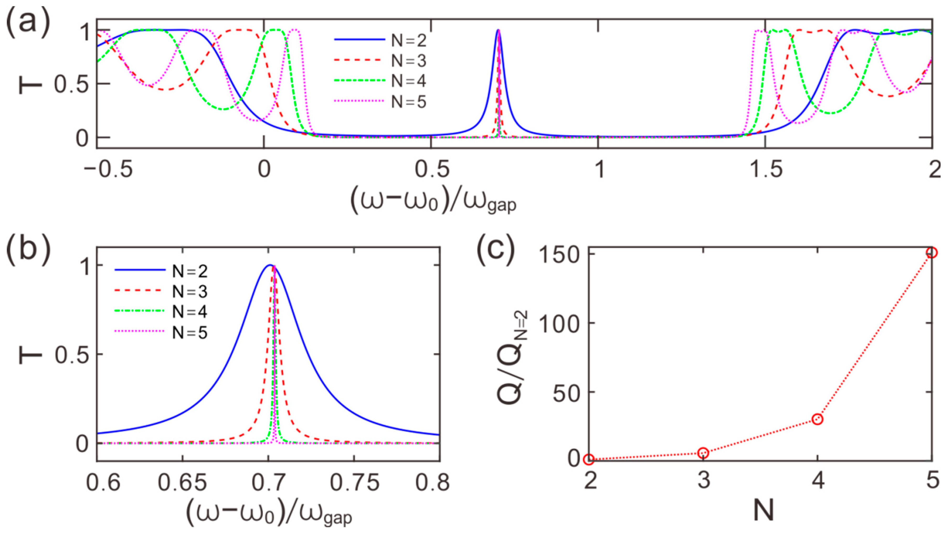
For different periodic numbers
N of system,
Figure 5a gives the corresponding transmission spectra of light waves. The parameters are set as
Te = 100 K and
P = 100 GPa, respectively. One can see that the bandgap and resonant defect mode are still supported in these structures for different values of
N. The bandgap edge becomes steeper as
N increases, and the resonant peak becomes sharper by adding the dielectric layers of the photonic crystal. Since the system can be viewed as a resonant cavity, the resonance and selectivity of defect mode were enhanced by improving the periodic number.
To observe the defect mode more clearly,
Figure 5b demonstrates the detailed view profile of the transmitted peak of light waves for
N = 2, 3, 4, and 5. Obviously, for a larger
N, the peak of transmittance is narrower, viz., the resonance becomes stronger. Otherwise, the central resonant wavelength vibrates slightly as the periodic number changes. The dielectric layers increase by promoting
N, and consequently the reflectivity of light is enhanced. Therefore, the light resonances of the system and the defect mode can be improved synchronously by regulating the periodic number of the system.
Figure 5c investigates the quality factor (Q-factor) of the resonant cavity varying with the periodic number
N. The Q-factor is defined as the reciprocal of the half width for each transmission peak. It shows that the normalized Q-factor of the resonant cavity increases exponentially with the increase in
N. The monochromaticity and selectivity of frequency are more excellent with a higher value of Q-factor.
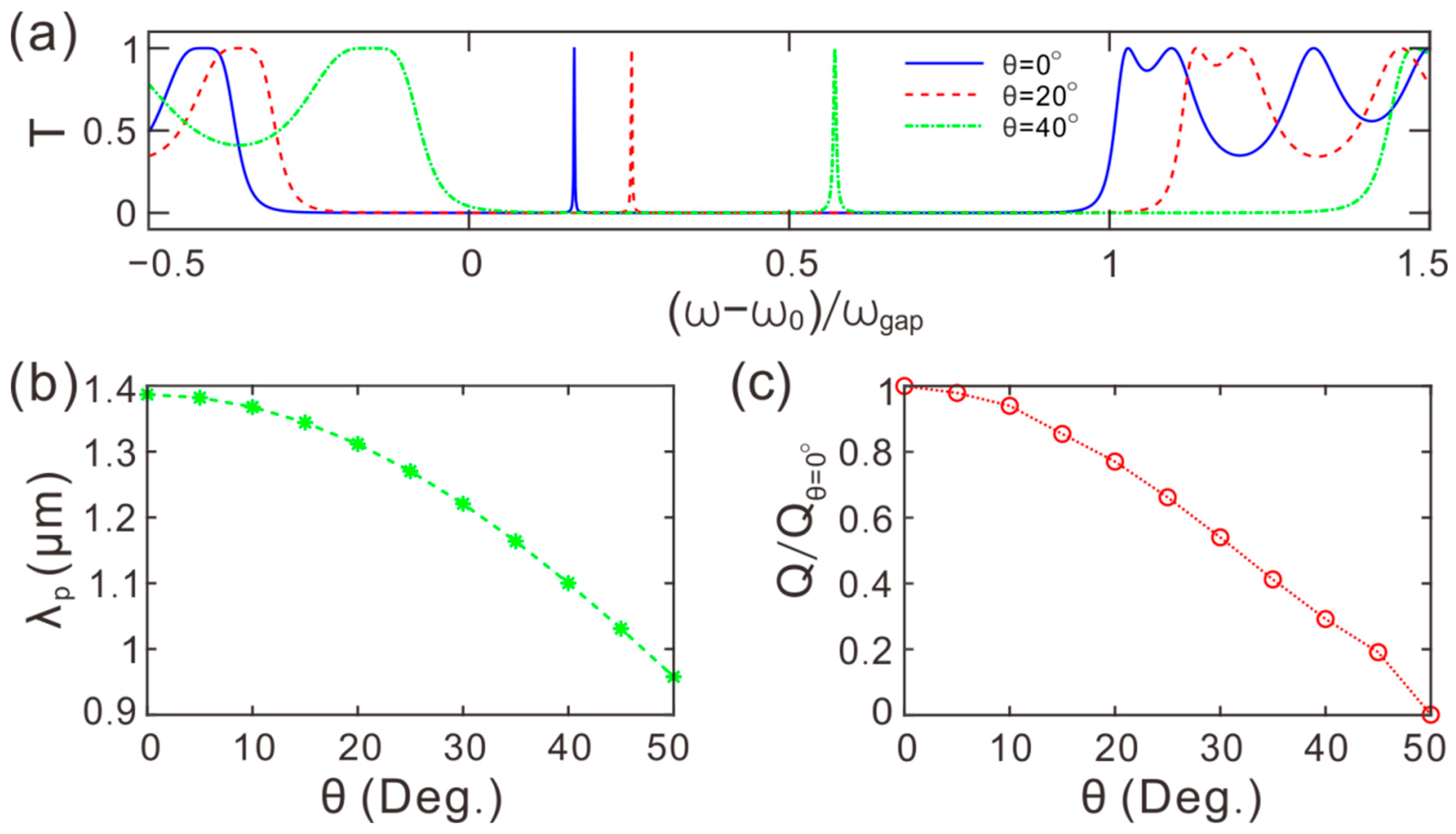
Changing the incident angle, the transmission spectrum of light waves also changes.
Figure 6a provides the transmittance varying with the normalized frequency for
θ = 0°, 20°, and 45°. The environment temperature is
Te = 100 K, and the intensity of pressure is set as
P = 100 GPa. By increasing the incident angle, one can see that the bandgap and defect mode are simultaneously moving toward the high-frequency direction. The interval between two adjacent peak enlarges as the incident angle grows. It can be further found that the resonant peak becomes wider, and the transmittance remains unchanged as the incident angle increases, so the resonance of the defect mode tends to become weaker by giving a larger value of
θ.
Figure 6b gives the central wavelength
λp of the defect mode changing with the incident angle. It has been shown that the transmission peak moves toward the right with respect to the normalized frequency axis as the incident angle increases. Simulation shows that the central wavelength
λp is inversely proportional to the incident angle and moves in the short wavelength direction. Therefore, the central wavelength of the resonant peak can be modulated by tuning the value of
θ.
Figure 6c explores the Q-factor of the resonant cavity changing with the incident angle. The Q-factor is the same as the definition in
Figure 5c. It has been mentioned that the transmission peak becomes wider as the incident angle grows, so one can see that the Q-factor of the defect cavity decreases with the increase in the incident angle. This means that weak selectivity of frequency and terrible monochromaticity of the defect mode may be a result of modulating a larger incident angle.
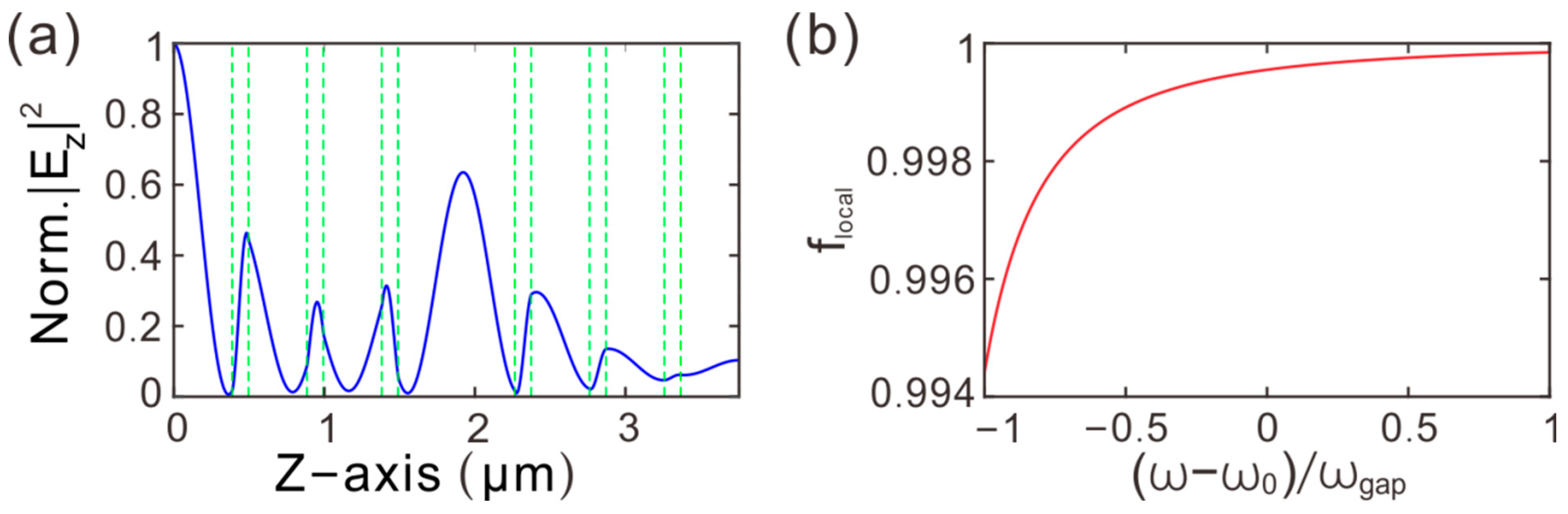
Figure 7a gives the electric field distribution of the defect mode. The environment temperature and pressure are set as
Te = 100 K and
P = 20 GPa, respectively. The incident angle is given by
θ = 20°. The central wavelength of the defect mode in the transmission spectrum is
λp = 1.4709 μm. In this case, the refractive indices of HgBa
2Ca
2Cu
3O
8+δ and GaAs are n
a = 0.9994 and n
b = 3.5123, respectively. One can see that the power of the electric field is mainly restricted in the defect layer in the center. The symbol of
Ez is the component of the electric field along the propagating direction. We normalized the field to demonstrate the distribution of power conveniently. The field distribution is asymmetric to the center point, resulting from the thickness shrinkage of dielectric layers on which the hydrostatic pressure is applied.
In the polarized dielectrics, the local field
Elocal presents the electric field acting on an atom or molecule in dielectrics. The difference between
Elocal and the macroscopic field
E is denoted by the local correction factor correction factor
flocal. For a resonant cavity, the effective local field for the polarization is expressed as
where
ε is the permittivity of the material of the resonant cavity [
31]. Therefore, the local field correction factor is given by
The whole superconducting photonic crystal can be viewed as a resonant cavity and the defect local at the center is the body of cavity. Since the permittivity of the material of defect, viz., the superconductor HgBa2Ca2Cu3O8+δ, is a function of the incident wavelength of light, the local field correction factor changes with the wavelength as well.
Figure 7b explores the local field correction factor varying with the frequency of light waves. It shows that the correction factor of local field increases with the increase in the normalized frequency. The value of the correction factor is
flocal = 0.9944, and it tends to saturate as the normalized frequency increases. The saturation value of the local field correction factor is approaching 1. The factor
flocal can be utilized for correcting the local field of defect mode, which makes the distribution of the electric field more precise. However, the conclusion of the main power of the defect mode locating at the central defect is unchanged.
Two trapezoid waveguides are local at both sides of the photonic crystal, which apply the hydrostatic pressure on the structure and transmit light beams out synchronously. The three low-loss windows are at near-IR range, so we set the operating wave length of pressure sensing around 1.55 μm to transmit the sensing information in the fiber. The absolute pressure sensitivity can be as high as 2.6 nm/GPa at the hydrostatic pressure of 6 GPa, which is higher than the maximum 1.7 nm/GPa in the investigation [
21].


 ,
, 


