Article

Properties of ScAlMgO4 as Substrate for Nitride Semiconductors

1
New Industry Creation Hatchery Center, Tohoku University, Sendai 980-8579, Japan
2
Application Department, X-ray Division, Bruker Japan K.K., Yokohama 221-0022, Japan
3
Institute for Materials Research, Tohoku University, Sendai 980-8577, Japan
4
Department of Electronics, Kyoto Institute of Technology, Kyoto 606-8585, Japan
5
Graduate School of Science and Technology, Hirosaki University, Hirosaki 036-8224, Japan
6
Fukuda Crystal Laboratory, Sendai 989-3204, Japan
*
Author to whom correspondence should be addressed.
Present address: National Institute of Advanced Industrial Science and Technology, Tsukuba 305-8569, Japan.
He passed away in November 2021.
Crystals 2023, 13(3), 449; https://doi.org/10.3390/cryst13030449
Submission received: 22 December 2022 / Revised: 24 February 2023 / Accepted: 24 February 2023 / Published: 4 March 2023
(This article belongs to the Special Issue Research in GaN-based Materials and Devices)

Abstract

:
SCAM has been expected to be a suitable substrate for GaN blue-light-emitting-diodes (LEDs) and high-power high electron mobility transistors (HEMTs) because of its lower lattice mismatch to GaN than that of the widely used sapphire. Considering both potential device applications, the crystal lattice and optical properties of SCAM substrates were investigated on selected high quality samples. As lattice parameters, the thermal expansion coefficient as well as the lattice constant were extrapolated from room temperature to 2000 °C by using a high temperature X-ray diffraction (XRD) system with the heating unit on a sample stage. The thermal conductance, which is also important for growing bulk SCAM crystals and the operation of devices on the SCAM substrate, was measured. Raman scattering measurements were carried out to better understand crystal lattice characteristics. It was clearly confirmed that prepared SCAM crystals were of high quality. Similar to sapphire, SCAM has the high transparency over the wide wavelength range from ultraviolet to mid-infrared. The refractive index, important for the design of any optical devices, was measured. From these results, it can be said that SCAM is a suitable substrate for nitride devices, especially LEDs and solar cells.

1. Introduction

The nitride semiconductor InGaAlN has been commonly used for the fabrication of blue-light-emitting-diodes (LEDs) and high electron mobility transistors (HEMTs). This nitride semiconductor has progressed in a different way from conventional semiconductors such as Si and GaAs because even most representative GaN among nitride semiconductors has no bulk substrate. Usually, LEDs have been fabricated on sapphire substrates with a lattice-mismatch of 13.8% to GaN. HEMTs for base stations of cellular phones have been fabricated on SiC substrates with larger thermal conductivity than sapphire. Concurrently to device applications of nitride semiconductors, several methods for growing bulk GaN and AlN have been studied. Recently, the sample shipment of GaN wafers grown with the ammonothermal method has begun [1]. The dislocation density of these wafers is only 102−3/cm2. On the other hand, very thick GaN films have been grown on foreign substrates such as GaAs and sapphire substrates with halide vapor phase epitaxy (HVPE), the growth rate of which is nearly one order magnitude larger than that of the ammonothermal method, and free-standing GaN wafers have been fabricated. Actually, these wafers have been used for the fabrication of laser diodes with a wavelength of 405 nm for Blu-ray systems. This fabrication yield of free-standing GaN wafers is not so high because the separation of about 500 µm-thick GaN from a foreign substrate is not easy, especially since both mismatches of the lattice constant and thermal expansion coefficient are large, and the dislocation density is as high as 105−6/cm2. In 1995, C.D. Brandle et al. proposed ScAlMgO4 (hereafter shortly called SCAM) as a better foreigner substrate option than sapphire and GaAs for III-nitrides heteroepitaxial films deposition, considering its small lattice-mismatch of 1.8% [2]. In the following year, Hellman et al. successfully grew small SCAM single crystals [3]. However, it was very difficult to enlarge the crystal size. In 2010, he started the investigation of methods to produce large SCAM crystals at Fukuda crystal research laboratory.
In 2011, the first author of this paper, T. Matsuoka, began a research collaboration with T. Fukuda to develop large area SCAM crystals. The epitaxial growth of GaN on a SCAM substrate was performed by using molecular beam epitaxy (MBE) [3] and metalorganic vapor phase epitaxy (MOVPE) [4]. In 2017, a high quality flat-surface GaN/SCAM template was realized [5]. Blue light-emitting-diodes (LEDs) were also fabricated on SCAM substrates [6]. Even the fabrication of free-standing GaN substrates was attempted with HVPE by using SCAM [7]. In this case, the spontaneous separation based on the cleavability of SCAM during cooling down after growth was used. The cleavage plane was crystallographically confirmed using the X-ray crystal truncation rod scattering method [8]. The SCAM substrate separated from GaN was reported to be reusable [9]. It is demonstrated here that the SCAM crystal is a useful substrate for nitride devices development.
The crystal structure of SCAM was investigated by X-ray diffraction analyses and X-ray topography [10]. Further development of SCAM crystals will require full understanding of their properties, in particular, for the device applications of SCAM.
In this paper, the characteristics of SCAM with respect to lattice-constant, thermal expansion coefficient, thermal conductivity, and optical characteristics, which are indispensable for the device applications of SCAM, are systematically described. For obtaining accurate data, the samples were prepared from the central part of a wafer, which was cut out from a boule larger than 60 mm in diameter because SCAM crystals were often inhomogeneous in their composition. The data obtained here will be also useful for device applications of SCAM.

2. Sample Preparations

Bulk SCAM single crystals were grown by Czochralski (CZ) method using a furnace heated with high-frequency induction. As source materials, Sc2O3, Al2O3, and MgO with purity higher than 99.9% were used. Compositions of raw materials were determined so that SCAM with the stoichiometric ratio was grown. These materials were soaked in an iridium crucible. The atmospheric gas in the furnace was kept with mixture gases of nitrogen and oxygen. The seed was SCAM with a longitudinal direction along <0001>. The growth temperature was 1800 to 1950 °C. The pulling speed and the rotational speeds were 0.5 to 2.5 mm/h and 1 to 20 rpm, respectively. The precise growth conditions have been reported in the literature [11].
The grown bulk SCAM crystal was larger than 60 cm in diameter. However, the area with homogeneous composition was almost 2 inches in diameter. The samples for the following measurements were prepared from the central part of a wafer, which was cleaved out from a boule. The sample quality including its composition can be thought to be higher than that previously used for the measurements of SCAM properties.

3. Properties of SCAM

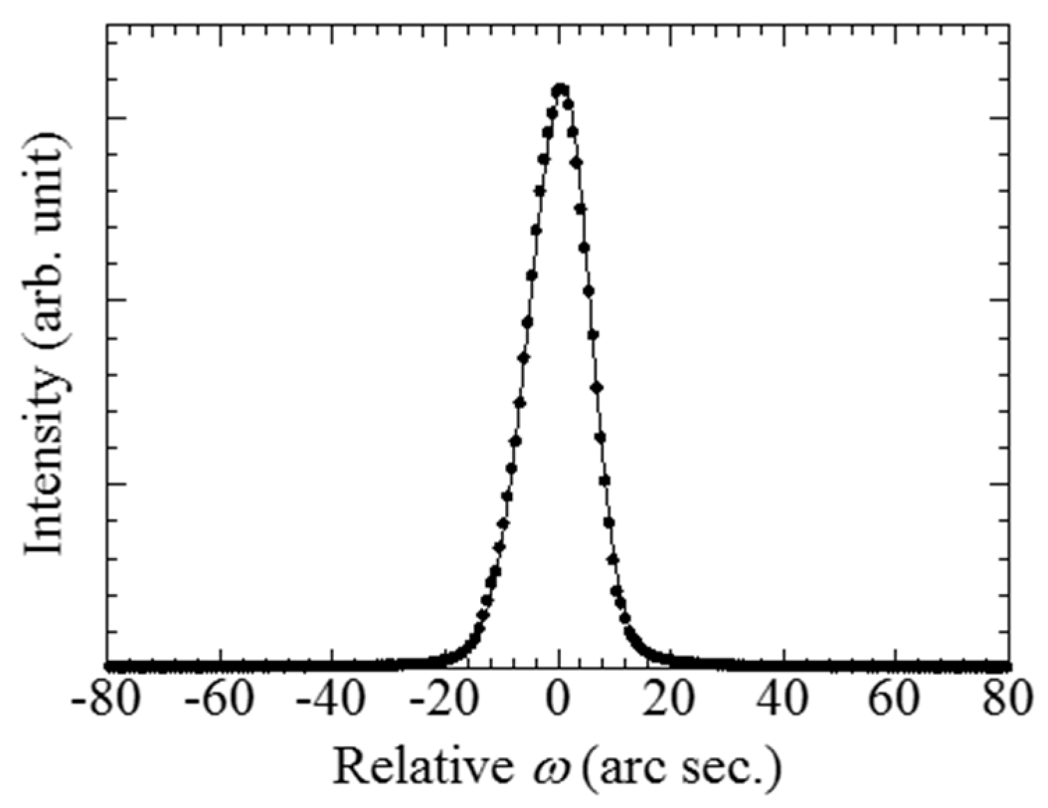
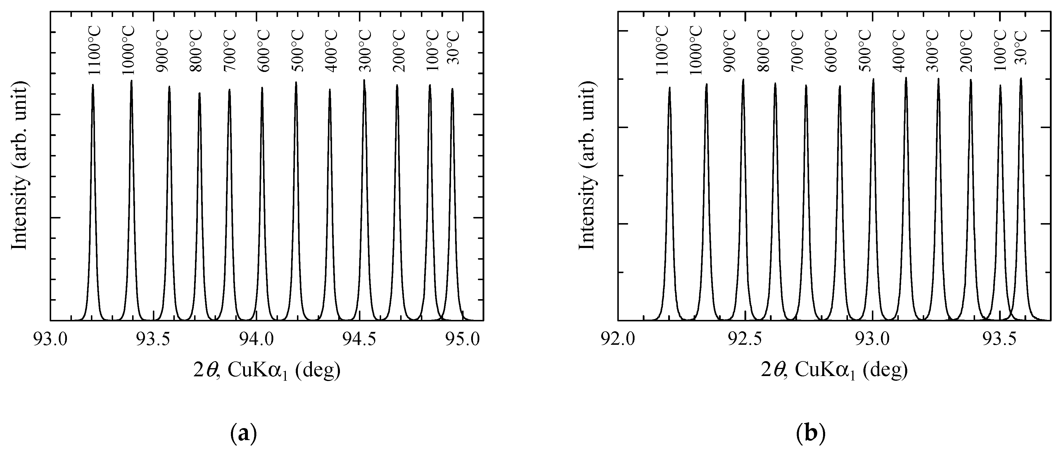
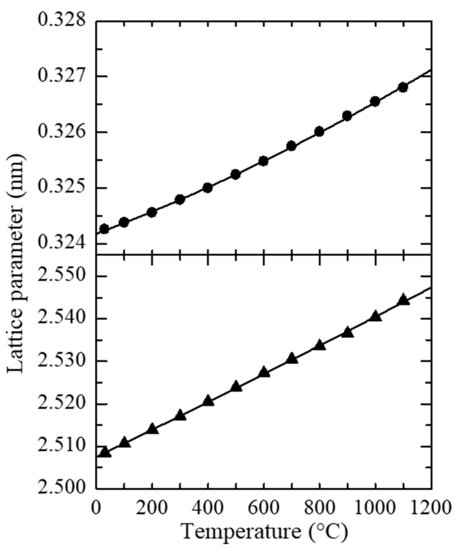
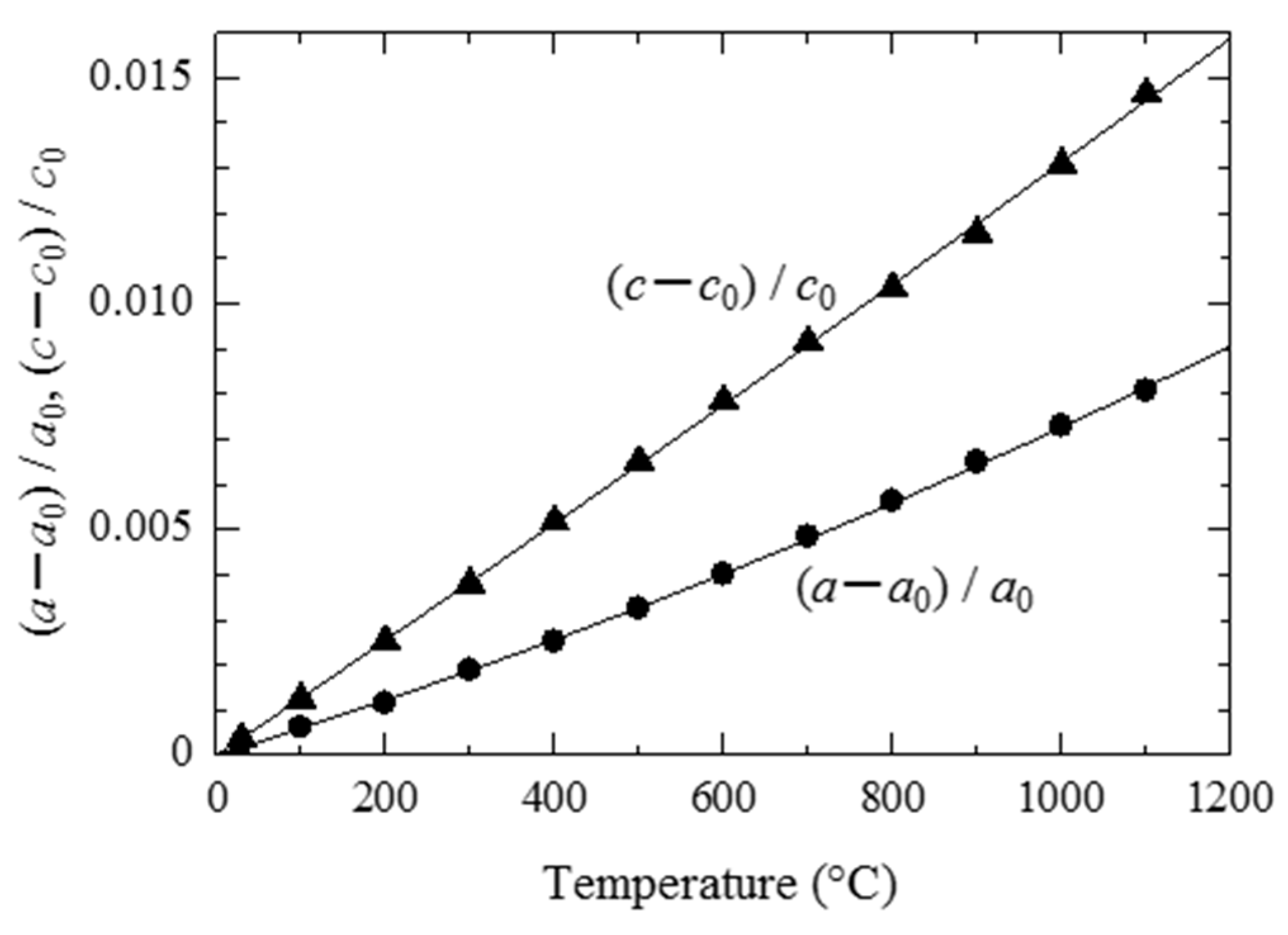
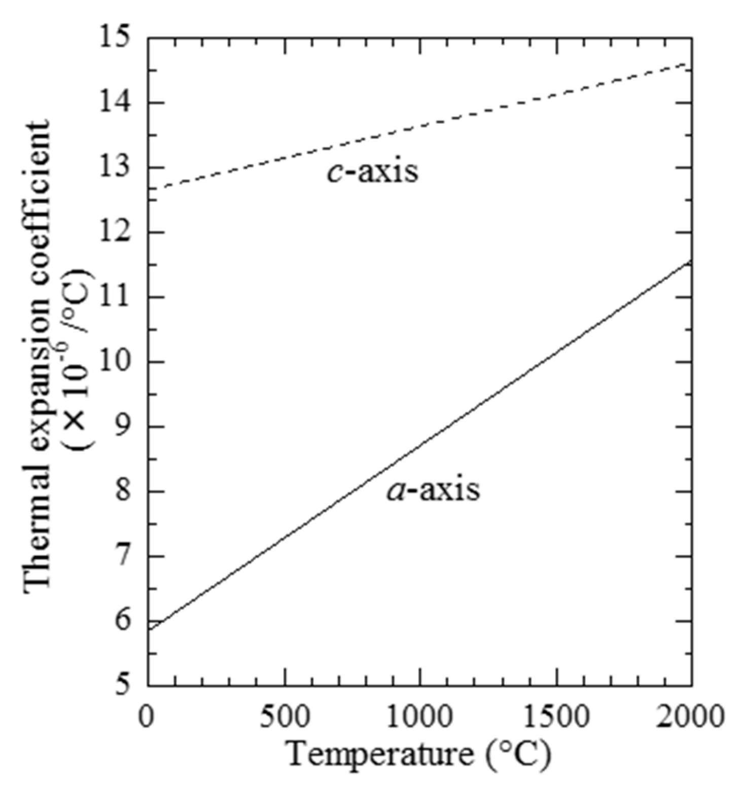
3.1. Lattice Constant and Thermal Expansion Coefficient

High temperature X-ray diffraction (XRD) measurement, which was performed on a high-resolution X-ray diffractometer (Bruker AXS D8 DISCOVER), was employed for the thermal expansion coefficient (TEC) of a (0001)-oriented SCAM single crystal. To obtain the lattice parameters, the high-resolution 2θω scans were performed around two specific diffraction peaks, 00,024 and 11 2 ¯ 18, because they can be observed at relatively higher 2θ angle, >90°, with higher relative intensities. The lattice parameters of a- and c-axes were calculated from both diffraction peaks using the following equations for the hexagonal crystal symmetry, respectively.
1 d h k i l 2 = 4 3 h 2 + h k + k 2 a 2 + l 2 c 2
In this study case,
1 d 000 24 ¯ 2 = 24 2 c 2 ,   1 d 11 2 ¯ 18 ¯ 2 = 4 a 2 + 18 2 c 2
The 00,024 diffraction was measured with the symmetric geometry as the same as the so-called 2θω configuration. The 11 2 ¯ 18 diffraction was measured with the grazing exit asymmetric geometry. The primary X-ray beam path uses a multilayered X-ray reflection mirror and a two-bounce Ge 004 channel-cut monochromator with the highest angular resolution less than 0.004° of FWHM at the Si 004 Bragg peak, which are mounted between the rotating anode X-ray source (6.0 kW of output) and the specimen to obtain highly parallel and monochromatized X-rays in the case of 2θ—ω measurements. The diffracted X-rays were analyzed by a one-bounce Ge 022 analyzer, which has the resolution of 0.005° in 2θ, and can eliminate the sample surface displacement errors caused by thermal expansion that are typically observed on powder X-ray diffractometers. To obtain the TEC of the specimen, the heating unit on a sample stage (Anton Paar DHS1100) was established. The temperature step was from room temperature up to 1100 °C with increments of 100 °C. The temperature deviation was smaller than 5 °C. The heating rate of the measurements was 20 °C/min and the temperature was stabilized for about 10 min before scanning.
Figure 1 shows the high-resolution rocking curve for 00,018 diffraction of a SCAM single crystal measured at room temperature. The observed rocking curve profile shows only a single, sharp and symmetric peak shape compared with previously reported spectra [12]. As a result, FWHM is defined as 0.0036° (12.99 arc seconds) by pseudo-Voigt function fitting, and its value is virtually corresponding to the instrumental resolution (<0.004°). FWHM values of the rocking curve profile have to be noticed to depend on the Bragg angle and its observed value was 0.0085° (30.49 arc seconds) around 0009 diffraction of SCAM. FWHM value also shows about 0.0033° (12 arc seconds, not shown here) narrow peak profile compared with previously reported results [12]. The present result demonstrates that the SCAM single crystal grown has excellent crystal perfection, the same as a single crystal Si by rocking curve results and no misoriented sub-grains in the X-ray irradiated area.
The high-resolution rocking curve scan results around the 00,018 diffraction peaks of a SCAM single crystal. The measurement results (dots) are fitted by a pseudo-Voigt function (solid line).
Figure 2a,b show the high-resolution 2θ—ω scans for 00,024 and 11 2 ¯ 18 diffractions for a (0001)-oriented SCAM single crystal acquired at various temperatures, respectively. Each diffraction peak was clearly moved to a lower angle due to the thermal expansion of the lattice parameters of a SCAM single crystal.
Figure 3 shows the temperature dependence of the a- and c-axes lattice parameters for a SCAM single crystal, and Table 1 summarizes each lattice parameter. The estimated errors of the lattice parameters are about ±0.00002 nm for all conditions due to the high angular resolution analyzer optics geometry [13]. The obtained lattice parameters of a- and c-axes are 0.32426(2) nm and 2.50850(2) nm at room temperature, and they are about 0.20% larger and 0.26% shorter than the published parameters a = 0.3236 nm and c = 2.515 nm, respectively [14]. The temperature dependences of both lattice parameters were smooth and no phase transition related glitches were observed. To our knowledge, there is no structural phase transition in SCAM crystals for this temperature range. In Figure 3, each dependence of the lattice parameters plotted against the temperature (Celsius; °C) was fitted by quadratic functions as follows: a (nm) = 4.6207 × 10⁻¹⁰ T2 + 1.8978 × 10⁻⁶ T + 0.32418 and c (nm) = 1.2355 × 10⁻⁹ T2 + 3.1700 × 10⁻⁷ T + 2.5076. These functions clearly show the lattice parameters at 0 °C (a0 and c0), that is, a0 = 0.32418 nm and c0 = 2.5076 nm.
To determine the TEC of a SCAM single crystal, the temperature dependence of the expansion ratio of a- and c-axes was figured out as shown in Figure 4. Each dependence was fitted by quadratic functions as follows, (aa0)/a0 = 1.4331 × 10⁻⁹ T2 + 5.8366 × 10⁻⁶ T and (cc0)/c0 = 4.9126 × 10⁻¹⁰ T2 + 1.2644 × 10⁻⁶ T. The derivative of the lattice constant normalized with lattice constant at 0 °C as shown in Figure 4 is equal to the TEC at each temperature. The temperature dependences of TEC for a SCAM single crystal are shown in Figure 5. Figure 5 clearly shows that the TECs of the a- and c-axes are linearly increasing with the temperature. The relationships are extrapolated up to 2000 °C, but the TEC of the c-axis shows smaller temperature dependence comparing with that of the a-axis. The temperature dependence of TECs are described with the following equations, TECa = 2.866 × 10⁻⁹ T + 5.837 × 10⁻⁶ (/°C) and TECc = 9.825 × 10⁻¹⁰ T + 12.64 × 10⁻⁶ (/°C). This study clearly established the anisotropy and temperature dependence of a- and c-axes TECs for a SCAM single crystal.

3.2. Thermal Conductance

For measurements of the thermal diffusivity α and the heat capacity Cp, rectangular specimens with 10 mm in length, 7.5 mm in width, and 0.53 mm in thickness were prepared by cutting from a SCAM single crystal ingot. α and Cp were measured by the laser flash method at room temperature using a TC-8000 apparatus (ULVAC-RICO). A single pulse sapphire laser with a 1.14 ms pulse width irradiated the specimen surface covered with graphite powder to generate the thermal flow detected by an infrared sensor. From the profile of the temperature change with time, α and Cp can be obtained [15,16,17]. The SCAM α and Cp values, measured at room temperature, were 0.014 ± 0.002 cm2 and 0.86 ± 0.03 J/g K (i.e., 138 ± 5 J/mol K), respectively. This value was in good agreement with 128.6 J/mol K calculated using Kopp’s law, which shows the linear relationship between the heat capacity of a solid and its elemental composition. The heat capacities of Sc2O3, Al2O3, and MgO used here are shown below.
Sc2O3: 103.7 J/mol K at 293 K [18];
Al2O3: 79.8 J/mol K at 293 K [19];
MgO: 36.8 J/mol K at 298 K [19].
The thermal conductivity λ was calculated from α, Cp, and the density ρ of the specimen, using the following equation.
λ = αCp ρ
Finally, from Equation (3), the room temperature SCAM λ value is 4.2 ± 0.2 W/m K.

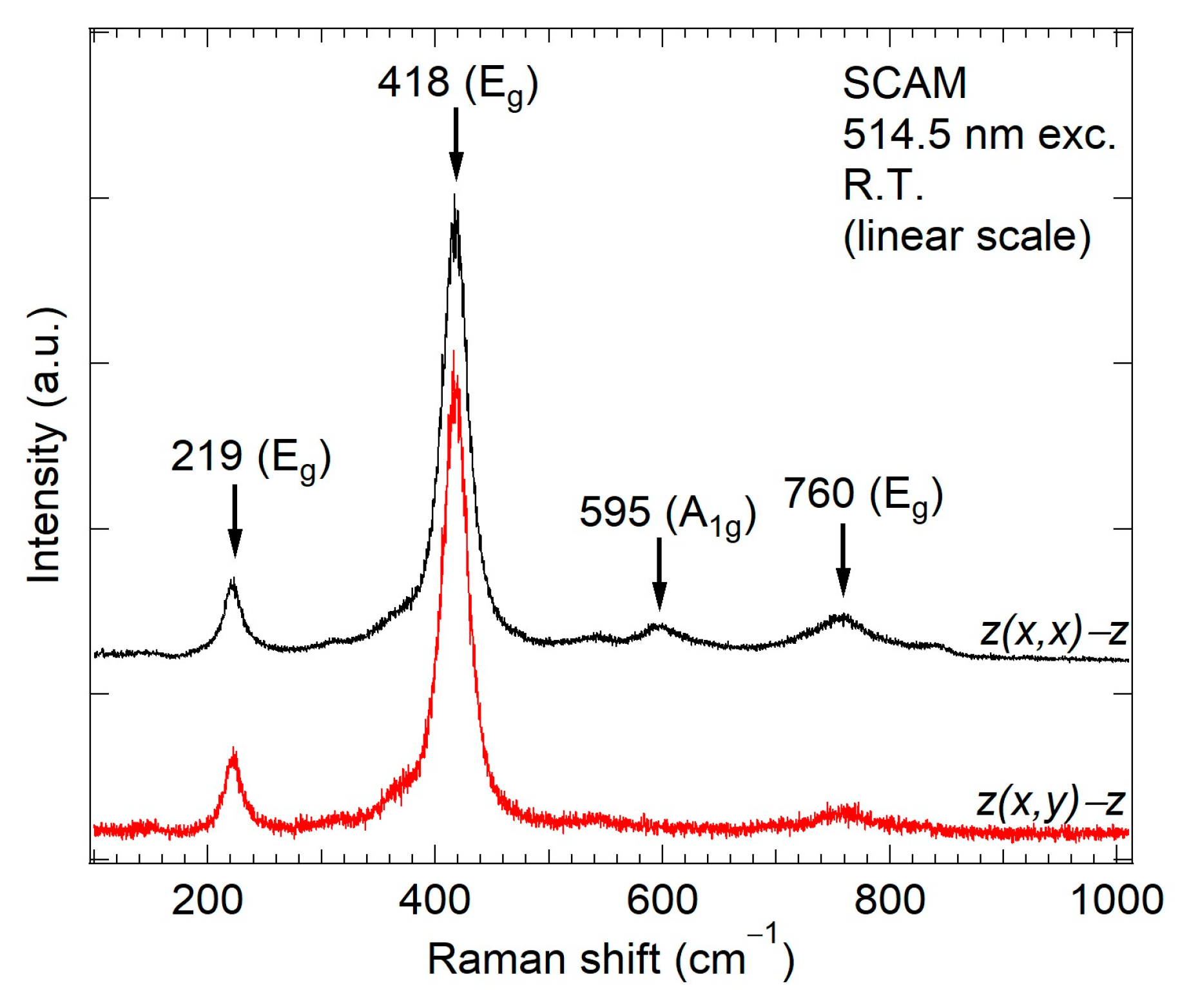
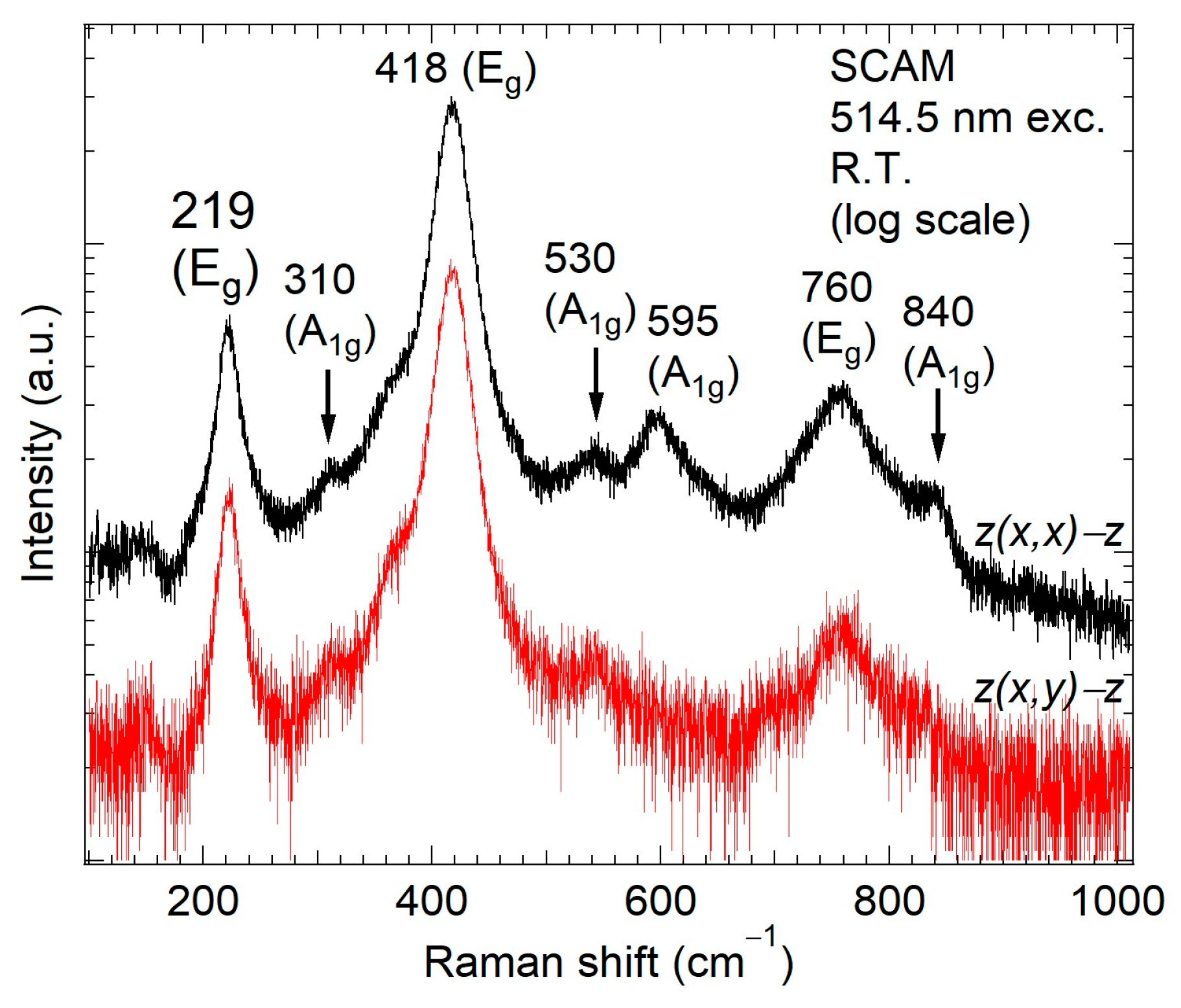
3.3. Raman Scattering Measurements

SCAM takes the crystal structure of the rare-earth iron oxide system, RFe2O4 (R = Lu and Yb) [20]. RFe2O4 is classified into the rhombohedral center-symmetric system with the space group D 3 d 5   ( R 3 ¯ m ) . In RFe2O4, the Fe3+ and Fe2+ ions occupy a crystallographically equivalent site with the same probability to form triangular lattice layers arranged in bilayers. The bilayers are separated by a triangular lattice layer including rare earth ions. In SCAM, likewise, the Al3+ and Mg2+ ions occupy an equivalent site, and are surrounded by four O atoms to form characteristic [AlMgO4]3− layers parallel to the ab plane. The layers are further connected into the 3-dimensional framework by the Sc atoms via O atoms between the layers [21,22]. In the case of RFe2O4, the primitive cell contains one formula unit, giving rise to a total of 21 phonon branches. A group theoretical analysis then yields phonon modes 3A1g + 3Eg + 4A2u + 4Eu at the Γ-point [23]. Here, the 3A1g + 3Eg modes are Raman active, 3A2u + 3Eu are IR active, and the remaining three, A2u + Eu, are acoustic modes. The Eg and Eu modes doubly degenerate. The Raman tensors for the six Raman-active modes are described as follows [24].
A 1 g = a a b ,   E g = c c d d ,   c d c c d
The present Raman analysis is based on this treatment for RFe2O4. To make the rigorous treatment for SCAM, all the possible atomic coordinations distinguishing between Al and Mg ions have to be considered. However, such a treatment is too complicated and not realistic.
The Raman scattering experiment was conducted at room temperature using an optical microscope and an Ar-ion laser at a wavelength of 514.5 nm for scattering. The polarized detection was tested for the phonon mode assignment. Backscattered photons were dispersed by a double-monochromator with a focal length of 85 cm for the spectral analysis. The Raman spectra were recorded by a liquid-nitrogen-cooled charge-coupled-device (CCD) camera.
Since SCAM single crystals can be cleaved in the ab-plane as layered materials, Raman scattering by back-scattering from the c-plane with parallel polarization z ( x , x ) z ¯ and crossed polarization z ( x , y ) z ¯ can be easily examined. The Raman tensors predict that both the A1g and Eg modes can be observed in the parallel configuration, whereas only the Eg modes can be observed in the crossed configuration. Figure 6 shows the observed Raman spectra of a SCAM crystal sample by back-scattering from the c-plane, where the upper and lower traces correspond to parallel and crossed polarization spectra, respectively. Four phonon peaks with mode assignments at 219 (Eg), 418 (Eg), 595 (A1g) and 760 cm−1 (Eg) can be easily identified. Weaker signals can be easily found and be compared with relative peak intensities by re-plotting the signal intensity in a logarithmic scale as shown in Figure 7. Here, additional A1g modes at 310 cm−1 and 840 cm−1 can be identified, and all the expected six Raman-active modes are lined up. The weak signal at 530 cm−1 has another possibility to be assigned to A1g mode. Other similar weaker signals by more careful inspection of the spectra may be found. However, such a detailed analysis is left as a remaining issue. In that case, the validity of the present Raman analysis based on the RFe2O4 structural model may also have to be reconsidered.

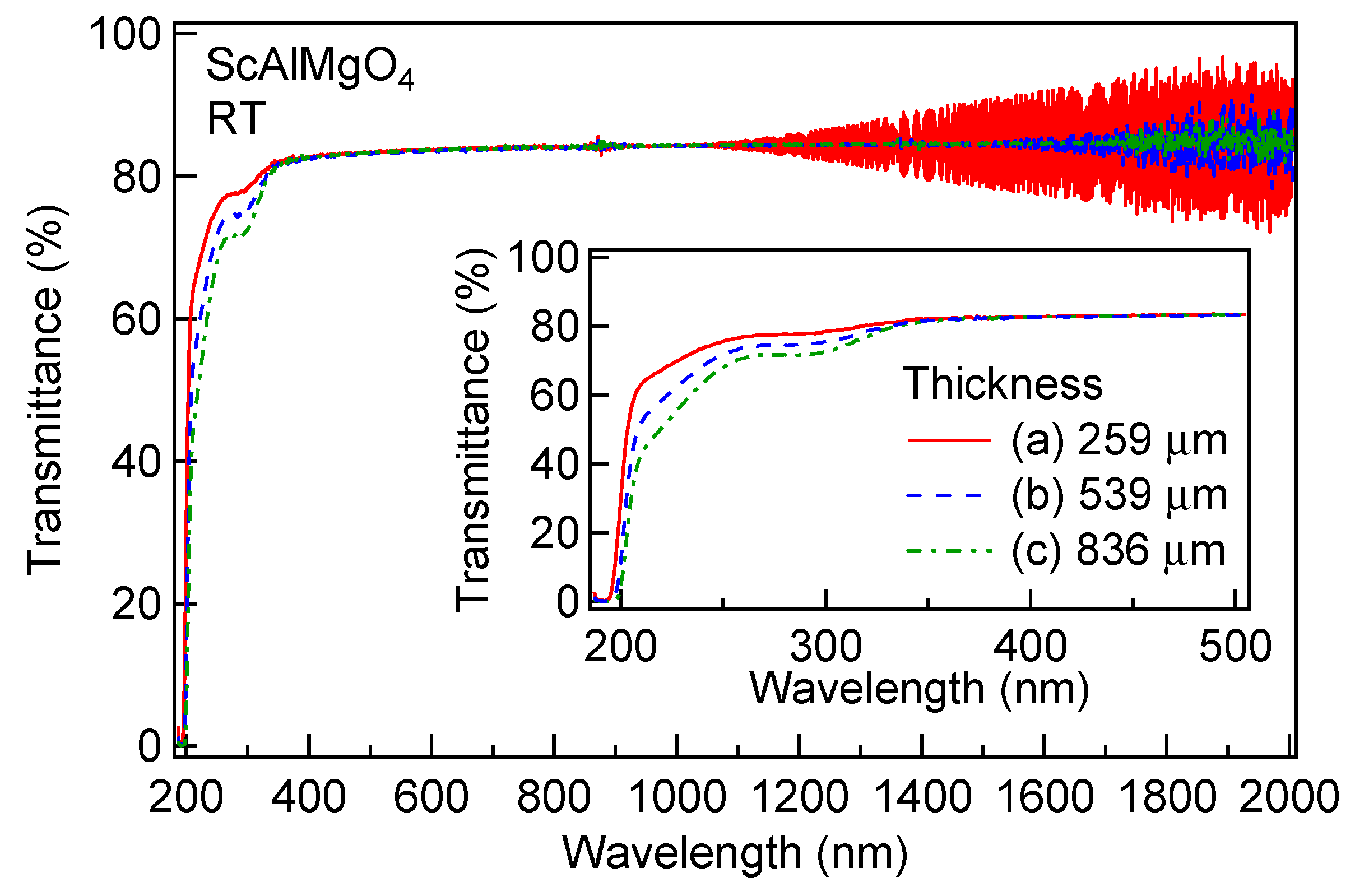
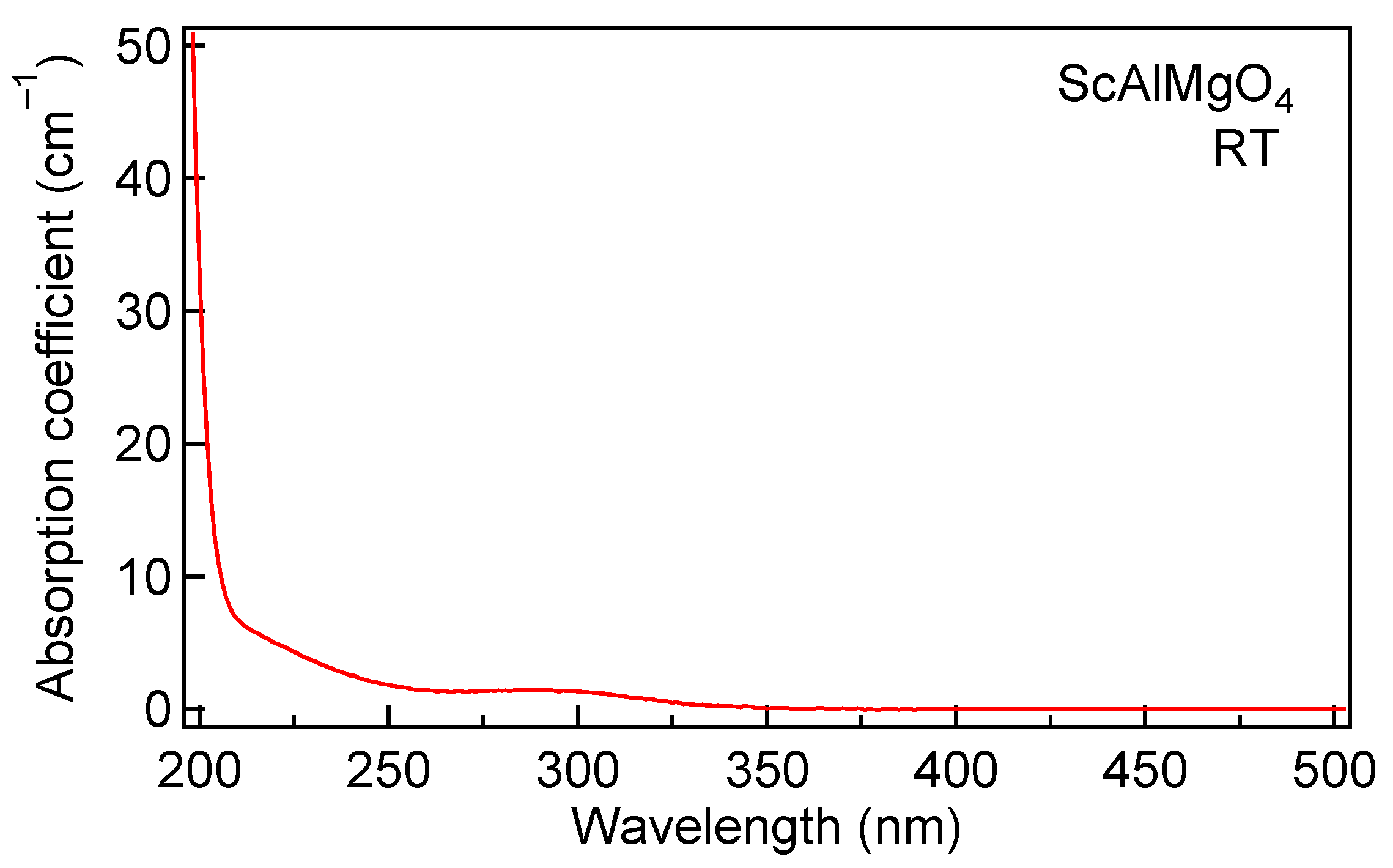
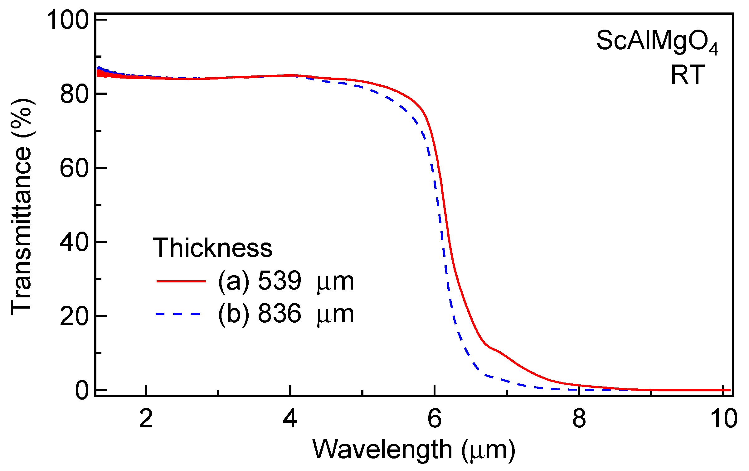
3.4. Optical Transmissions

Transmission spectroscopy measurements were performed from ultraviolet to near-infrared by SHIMADZU UV-VIS-NIR Spectrophotometer UV-3600 at room temperature (RT). Figure 8 shows the transmission spectra of SCAM substrates with the thickness of (a) 259 μm, (b) 539 μm, and (c) 836 μm. These substrates were prepared by cleaving the same SCAM boule at a (0001) face by a razor blade. In the transmission spectra, a small valley around 290 nm was observed. The transmission reduction around this wavelength was also reported in the literature for SCAM crystals grown by CZ method [12] and by floating zone method [25]. At the wavelength longer than around 370 nm, the transmittance of SCAM substrates was almost the same value above 80%. The spectral fringes observed at the wavelength longer than 1 μm is caused by the thin sample thickness.
Figure 9 shows the room-temperature absorption coefficient profile of SCAM calculated from the transmission spectral data shown in Figure 8. The absorption coefficient of the SCAM crystal gradually increases with decreasing the wavelength from around 370 nm. The profile shows a small band with a peak around 290 nm, which was observed as the small valley in the transmission spectra shown in Figure 8. It may be related to the crystalline quality of the SCAM crystal, because it has been reported that the absorption around 290 nm was reduced by the annealing in H2 ambience [12]. The crystallographic perfection of our sample may be higher because this absorption peak was relatively weaker.
The Fourier-transform infrared (FT-IR) transmission spectra measurements from near-infrared to mid-infrared were performed with a Bruker Optics Vertex 80 v at room temperature. The measurement was performed in a vacuum to avoid atmospheric absorption. Figure 10 shows the transmission spectra of SCAM substrates with the thicknesses of (a) 539 μm and (b) 836 μm. The transmission spectrum of the 259 μm-thick SCAM substrate is omitted from Figure 10 due to the strong spectral fringes originating from the thin sample thickness. At the wavelength longer than 4 μm, the transmittance decreased and the difference in the transmittance between the two samples was observed.
As a result of transmission spectroscopy measurements, the SCAM crystal was found to be optically transparent from the ultraviolet to mid-infrared range.

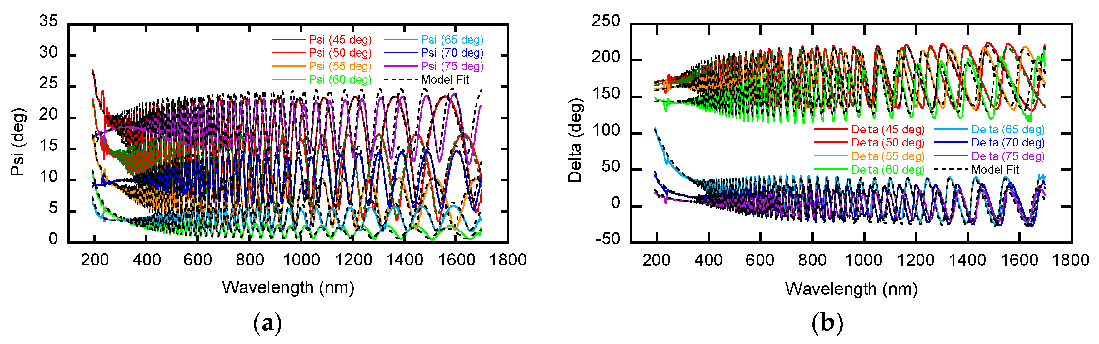
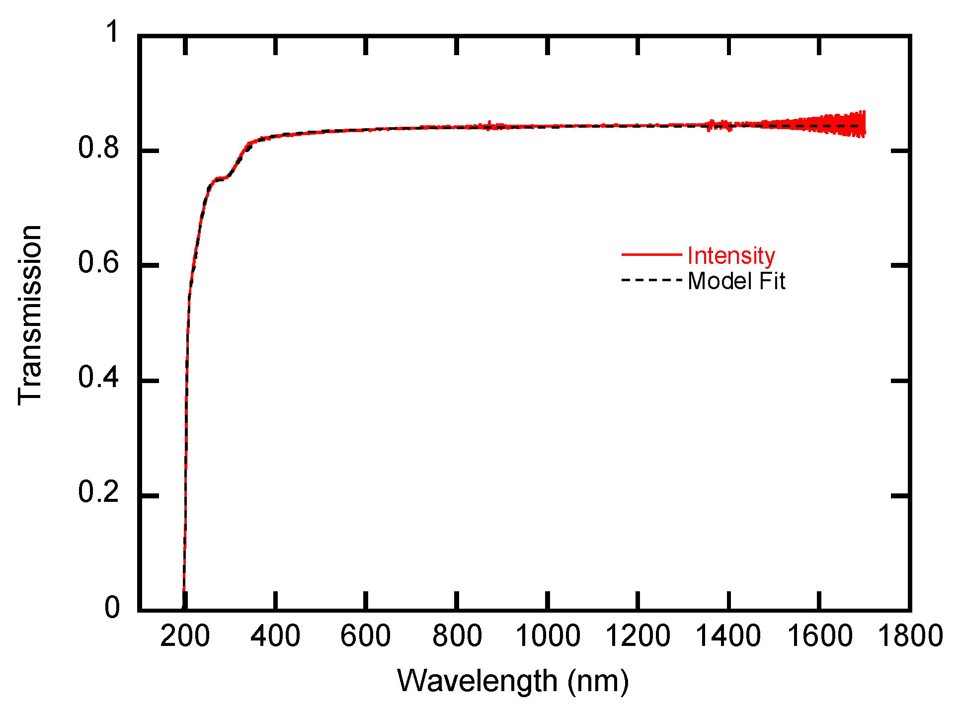
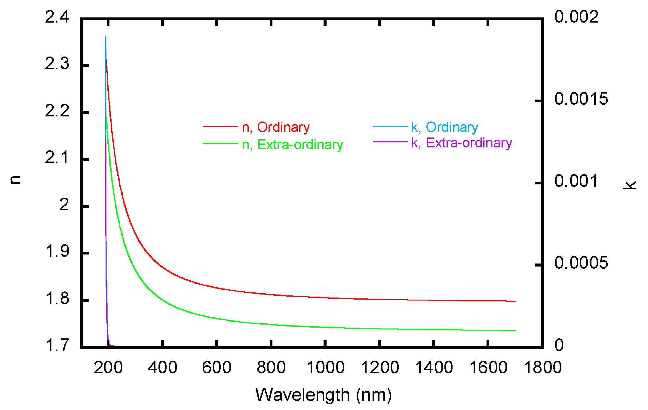
3.5. Refractive Index

Spectroscopic ellipsometry (SE) measurements were performed using a rotating-compensator instrument (J.A. Woollam, M-2000DI, 645 M Street Suite 102 Lincoln, NE 68508 USA) with a wavelength range of 193 to 1690 nm, and with incident angles of 45, 50, 55, 60, 65, 70, and 75 degrees. Ellipsometric data were analyzed using CompleteEase (J.A. Woollam, 645 M Street Suite 102 Lincoln, NE 68508 USA). By this program, all of the multi-angle ellipsometric data can be analyzed simultaneously and combined with the transmission data.
SE measurements were performed three times by rotating the SCAM substrate by 45 degrees to confirm the c-axis orientation. As the three spectra were completely matched with each other, the c-axis was confirmed to be perpendicular to the wafer surface. A series of measured SE data, Ψ and Δ, was shown in Figure 11a, b, respectively.
SE data were analyzed through the combination with the transmission data mentioned in the previous section. In this analysis, the dielectric function was modeled by a uniaxial-anisotropic material with three Gaussian oscillators for each direction, using the Gen-Osc function by CompleteEase program. Note that the program proves the Kramers–Kronig consistency. The fitting results for SE Ψ, Δ, and transmission were shown in Figure 11a,b and Figure 12, respectively.
Figure 13 shows the anisotropic optical constants obtained by the model fitting. Ordinary and extraordinary refractive indices (n) can be successfully determined. The extinction coefficient (k) in the wavelength range above 400 nm is characterized as zero, which is consistent with the results from the transmission measurements mentioned in the previous section.

4. Conclusions

In this paper, two kinds of representative properties in SCAM were measured, i.e., lattice properties and optical ones, considering the device applications of SCAM. The thermal expansion coefficient (TEC) as well as the lattice constant of substrates is the essential information for fabricating any device structures. In this paper, SCAM a- and c-axes TECs were measured and extrapolated from room temperature to 2000 °C using a high temperature XRD system with a heating unit on a sample stage. The lattice parameters of a- and c-axes were calculated from 11 2 ¯ 18 and 00,024 diffraction peaks. The lattice-constants of the a- and c-axes were almost the same as the previously reported values [23]. The TECs of the a- and c-axes were shown to be linearly increasing with the temperature up to 2000 °C. The TEC of the c-axis was also shown to have a smaller temperature dependence compared to that of the a-axis. Those TECs were directly observed on the wafer-shaped plate made of a bulk SCAM single crystal, and they are about 5.9% and 24.5% larger than powder SCAM crystals, which were crushed in an agate mortar for the a- and c-axes, respectively, at 30 °C [25]. However, the estimated TECs at 1200 °C were about 8.1% and 10.4% smaller than the reported values for the a- and c-axes [26]. This suggested that SCAM wafers with the shape of a plate actually show more linear thermal expansion under the deposition process.
The thermal conductance, which is also important for growing bulk SCAM crystals, heteroepitaxial deposition, and the operation of devices on SCAM substrates, was measured through the thermal diffusivity and the heat capacity experimentally obtained by a laser flash method at room temperature.
As one of the basic properties in crystals, the information of the lattice vibration modes was obtained by Raman scattering spectroscopy, which clearly verified the existent crystal symmetry.
The present work clearly addressed issues related to the SCAM transmittance spectral range. SCAM has high transparency over the wide wavelength range of ultraviolet to mid-infrared. Therefore, it can be said that SCAM is also suitable as a substrate for nitride devices such as LEDs and solar cells. The refractive index, important for the design of any optical devices, was measured. Its dependence on the wavelength obtained here will be useful.

Author Contributions

Conceptualization, T.M.; sample preparation, T.F.; measurements and analyses, H.M. for X-ray, S.S. for Thermal conductance, Y.O. and K.Y. for Raman scattering, S.K. for Optical transmissions, H.O. for Refractive index; writing—original draft preparation, H.M., H.M., S.S., Y.O., K.Y., S.K., and H.O.; writing—review and editing, T.M. All authors have read and agreed to the published version of the manuscript.

Funding

This research received no external funding.

Data Availability Statement

Not applicable.

Acknowledgments

The authors would like to thank Takanobu Satoh of J. A. Woollam Japan for the measurement of refractive index. While preparing this manuscript, one of the authors, Hiroshi Okamoto, passed away November 2021. All the authors pray that his soul may rest in peace. They also thank Noriyuki Hasuike of Kyoto Institute of Technology for clearly drawing Figure 6 and Figure 7.

Conflicts of Interest

The authors declare no conflict of interest.

References

  1. Kucharski, R.; Sochacki, T.; Lucznik, B.; Bockowski, M. Growth of bulk GaN crystals. J. Appl. Phys. 2020, 128, 050902. [Google Scholar] [CrossRef]
  2. Hellman, E.S.; Brandle, C.D.; Schneemeyer, L.F.; Wismann, D.; Brener, I.; Siegrist, T.; Berkstresser, G.W.; Buchanan, D.N.E.; Hartfrod, E.H. ScAlMgO4: An oxide substrate for GaN epitaxy. Mat. Res. Soc. Symp. Pro. 1996, 395, 51. [Google Scholar] [CrossRef]
  3. Hellman, E.S.; Brandle, C.D.; Schneemeyer, L.F.; Wiesmann, D.; Brener, I.; Siegrist, T.; Berkstresser, G.W.; Buchanan, D.N.E.; Hartford, E.H. ScAlMgO4: An oxide substrate for GaN epitaxy. MRS Internet J. Nitride Semicond. Res. 1996, 1, 1. [Google Scholar] [CrossRef] [Green Version]
  4. Iwabuchi, T.; Kuboya, S.; Tanikwa, T.; Hanada, T.; Katayama, R.; Minato, A.; Fukuda, T.; Matsuoka, T. Abstract of MOVPE Growth of GaN on ScAlMgO4 Substrate. In Proceedings of the Spring Meeting of Japan Society of Applied Physics, Aoyama Gakuin University, Tokyo, Japan, 17–20 March 2014. 18a-E13-8. [Google Scholar]
  5. Iwabuchi, T.; Kuboya, S.; Tanikawa, T.; Hanada, T.; Katayama, R.; Fukuda, T.; Matsuoka, T. Ga-polar GaN film gown by MOVPE on cleaved ScAlMgO4 (0001) substrate with millimeter-scale wide terraces. Phys. Stat. Sol. 2017, 214, 1607054. [Google Scholar]
  6. Ozaki, T.; Funato, M.; Kawakami, Y. InGaN-based visible light-emitting diodes on ScAlMgO4 (0001) substrates. Appl. Phys. Express 2015, 8, 062101. [Google Scholar] [CrossRef]
  7. Ohnishi, K.; Kanoh, M.; Tanikawa, T.; Kuboya, S.; Mukai, T.; Matsuoka, T. Halide vapor phase epitaxy of thick GaN films on ScAlMgO4 substrates and their self-separation for fabricating free-standing Wafers. Appl. Phys. Express 2017, 10, 101001. [Google Scholar] [CrossRef]
  8. Hanada, T.; Tajiri, H.; Sakata, O.; Fukuda, T.; Matsuoka, T. Characterization of the ScAlMgO4 cleaving layer by x-ray crystal truncation rod scattering. J. Appl. Phys. 2018, 123, 205305. [Google Scholar] [CrossRef]
  9. Ohnishi, K.; Kuboya, S.; Tanikawa, T.; Iwabuchi, T.; Yamamura, K.; Hasuike, N.; Harima, H.; Fukuda, T.; Matsuoka, T. Reuse of ScAlMgO4 substrates utilized for halide vapor phase epitaxy of GaN. Jpn. J. Appl. Phys. 2019, 58, SC1023. [Google Scholar] [CrossRef]
  10. Inaba, K.; Sugiyama, K.; Fujii, T.; Fukuda, T. X-ray diffraction analysis and X-ray topography of high-quality ScAlMgO4 substrates. J. Cryst. Growth 2021, 574, 126322. [Google Scholar] [CrossRef]
  11. Fukuda, T.; Shiraishi, Y.; Nanto, T.; Fujii, T.; Sugiyama, K.; Simura, R.; Iechi, H.; Tadatomo, K. Growth of bulk single crystal ScAlMgO4 boules and GaN films on ScAlMgO4 substrates for GaN-based optical devices, high-power and high-frequency transistors. J. Cryst. Growth 2021, 574, 126286. [Google Scholar] [CrossRef]
  12. Tang, H.; Xu, J.; Dong, Y.; Lin, H.; Wu, F. Study on growth and characterization of ScAlMgO4 substrate crystal. J. Alloys Compd. 2009, 471, L43–L46. [Google Scholar] [CrossRef]
  13. Fewster, P.F.; Andrew, N.L. Absolute lattice-parameter measurement. J. Appl. Crystallogr. 1995, 28, 451–458. [Google Scholar] [CrossRef]
  14. Kimizuka, N.; Mohri, T. Structural classification of RAO3(MO)n compounds (R=Sc, In, Y, or lanthanides; A=Fe(III), Ga, Cr, or Al; M =divalent cation; n = 1–11). J. Sol. Stat. Chem. 1989, 78, 98–107. [Google Scholar] [CrossRef]
  15. Parker, W.J.; Jenkins, R.J.; Butler, C.P.; Abbott, G.L. Flash method of determining thermal diffusivity, heat capacity, and thermal conductivity. J. Appl. Phys. 1961, 32, 1679–1684. [Google Scholar] [CrossRef]
  16. Cape, J.A.; Lehman, G.W. Temperature and finite pulse-time effects in the flash method for measuring thermal diffusivity. J. Appl. Phys. 1963, 34, 1909–1913. [Google Scholar] [CrossRef]
  17. Taylor, R.E.; Cape, J.A. Finite pulse-time effects in the flash diffusivity technique. Appl. Phys. Lett. 1964, 5, 212–213. [Google Scholar] [CrossRef]
  18. Zakurdaev, A.; Huang, X. Experimental study of phase transformation and specific heat of ternary zirconia-based oxides using differential scanning calorimetry. J. Alloys Compd. 2009, 488, 469–499. [Google Scholar] [CrossRef]
  19. Kubaschewski, O.; Alcock, C.B. Metallurgical Thermochemistry, 5th ed.; Pergamon Press: Oxford, UK, 1979; pp. 268–356. [Google Scholar]
  20. Hou, Y.; Yao, Y.P.; Dong, S.N.; Teng, M.L.; Sun, X.F.; Lia, X.G. Temperature dependence of phonon spectra and structural characteristics in multiferroic LuFe2O4 system. J. Raman Spectrosc. 2011, 42, 1695–1700. [Google Scholar] [CrossRef]
  21. Errandonea, D.; Kumar, R.S.; Ruiz-Fuertes, J.; Segura, A.; Haussühl, E. High-pressure study of substrate material ScAlMgO4. Phys. Rev. B 2011, 83, 144104. [Google Scholar] [CrossRef] [Green Version]
  22. Zhou, H.-T.; Liang, Y.; Huang, W.-X.; Ye, N.; Zou, Y.-Q. Single-crystal structure of ScAlMgO4. Chin. J. Struc. Chem. 2009, 28, 947–950. [Google Scholar]
  23. Harris, A.B.; Yildirim, T. Charge and spin ordering in the mixed-valence compound LuFe2O4. Phys. Rev. B 2010, 81, 134417. [Google Scholar] [CrossRef] [Green Version]
  24. Loudon, R. The Raman effect in crystals. Adv. Phys. 1964, 13, 423–482. [Google Scholar] [CrossRef]
  25. Yanagida, T.; Koshimizu, M.; Kawano, N.; Okada, G.; Kawaguchi, N. Optical and scintillation properties of ScAlMgO4 crystal grown by the floating zone method. Mater. Res. Bull. 2017, 95, 409–413. [Google Scholar] [CrossRef]
  26. Simura, R.; Sugiyam, K.; Nakatsuka, A.; Fukuda, T. Erratum: High-temperature thermal expansion of ScAlMgO4 for substrate application of GaN and ZnO epitaxial growth. Jpn. J. Appl. Phys. 2016, 55, 099201. [Google Scholar] [CrossRef]
Figure 1. High-resolution rocking curve scan result around 00,018 diffraction peak of SCAM single crystal. The measurement results (dots) are fitted by pseudo-Voigt function (solid line).
Crystals 13 00449 g001
Figure 2. High-resolution 2θω scan results with various sample temperatures measured around (a) 00,024 and (b) 11-218 diffraction peaks of SCAM single crystal.
Crystals 13 00449 g002
Figure 3. Temperature dependence of the lattice parameters of a- and c-axes for SCAM crystal. The fitted lines with quadratic functions are also shown in this figure as a guide for your eyes.
Crystals 13 00449 g003
Figure 4. Temperature dependence of expansion ratio of a- and c-axes for SCAM crystal.
Crystals 13 00449 g004
Figure 5. Temperature dependence of thermal expansion coefficients (TECs) of a- and c-axes for SCAM crystal. The linear relationships of them are extrapolated up to 2000 °C.
Crystals 13 00449 g005
Figure 6. Raman spectra of SCAM by back-scattering from the c-plane with parallel (upper) and crossed (lower) polarization plotted in linear scale.
Crystals 13 00449 g006
Figure 7. Raman spectra of SCAM by back-scattering from the c-plane with parallel (upper) and crossed (lower) polarizations plotted in logarithmic scale.
Crystals 13 00449 g007
Figure 8. Room-temperature transmission spectra of SCAM substrates with the thickness of (a) 259 μm, (b) 539 μm, and (c) 836 μm. The inset figure was the expanded ultraviolet transmission spectra.
Crystals 13 00449 g008
Figure 9. Room-temperature absorption coefficient profile of the SCAM crystal calculated from the transmission spectra.
Crystals 13 00449 g009
Figure 10. FT-IR transmission spectra of SCAM substrates with thicknesses of (a) 539 μm and (b) 836 μm measured at room temperature.
Crystals 13 00449 g010
Figure 11. Experimental SE spectra of (a) Ψ and (b) Δ, and fitting spectra (dashed line).
Crystals 13 00449 g011
Figure 12. Experimental transmission spectrum (solid line), and fitting spectrum (dashed line).
Crystals 13 00449 g012
Figure 13. Anisotropic optical constants obtained by the model fitting.
Crystals 13 00449 g013
Table 1. Obtained lattice parameters of a- and c-axes for SCAM single crystal with various temperatures. The standard errors of the last digit are also shown in brackets.
TemperatureLattice Parameter
(°C)a (nm)c (nm)
300.32426(2)2.50850(2)
1000.32438(2)2.51070(2)
2000.32456(2)2.51390(2)
3000.32479(2)2.51711(2)
4000.32500(2)2.52053(2)
5000.32524(2)2.52388(2)
6000.32548(2)2.52725(2)
7000.32575(2)2.53052(2)
8000.32601(2)2.53351(2)
9000.32629(2)2.53655(2)
10000.32655(2)2.54039(2)
11000.32680(2)2.54431(2)
Disclaimer/Publisher’s Note: The statements, opinions and data contained in all publications are solely those of the individual author(s) and contributor(s) and not of MDPI and/or the editor(s). MDPI and/or the editor(s) disclaim responsibility for any injury to people or property resulting from any ideas, methods, instructions or products referred to in the content.

