1. Introduction
Over the last two decades, gallium nitride (GaN) has emerged as a strong candidate to develop electronic devices in high-power fast-switching applications due to its superior material properties such as high critical field, high saturation velocity, and high thermal conductivity [
1]. In general, GaN-based power transistors are fabricated either in lateral-type devices using foreign substrates such as Si, SiC, and sapphire, or in vertical-type devices grown on a homogeneous GaN substrate [
2]. Compared to the typical lateral GaN device high electron mobility transistor (HEMT), vertical power device topologies allow higher off-state blocking capability since the breakdown voltage scales with the drift layer thickness while maintaining a more uniform electric field distribution [
3,
4,
5].
To date, various three-terminal GaN vertical devices have been successfully developed, such as metal oxide semiconductor field effect transistors (MOSFETs) [
6], static induction transistors (SITs) [
7], and current aperture vertical electron transistors (CAVETs) [
8,
9,
10]. Among the various vertical power transistors, CAVET is unique in its merging of a lateral 2DEG channel with a vertical drift region. A CAVET device, therefore, efficiently takes the benefit of high current density and high breakdown voltage inherent to the vertical structure while combining the advantage of the high conductivity of polarization-induced 2DEG at the AlGaN/GaN interface in HEMTs [
11]. This feature of CAVETs makes it especially attractive to offer high current density in vertical devices.
The formation of p-type GaN films is a key technology in developing vertical power devices, and magnesium (Mg) is a commonly-used acceptor dopant in GaN. Among the reported CAVET studies, many of them inserted a p-GaN layer as the carrier blocking layer (CBL) with Mg doping either by metal-organic chemical vapor deposition (MOCVD) or by ion-implantation, to form a p-n body junction in the bulk for sustaining the blocking field in the off-state. However, there is a widely observed problem with the Mg-doped p-GaN layer sandwiched between the n-type or unintentionally doped (UID) GaN layers called the “memory effect”, whereby Mg inevitably out-diffuses into adjacent regions during the growth process at high temperatures [
12]. The CAVET structure consists of two growth steps, including the first p-i-n substrate growth and the second AlGaN/GaN heterostructure regrowth. During the high-temperature regrowth, Mg dopants from the p-GaN CBL are commonly observed to be heavily incorporated into the subsequent layers, and the formation of 2DEG is hindered by Mg propagation and redistribution to the vicinity of the regrown channel region, resulting in a drastic decrease in the current density level of the device. Lee et al. [
13] demonstrated by experiments that the 2DEG completely disappeared when the AlGaN/GaN layers were directly regrown on the Mg-doped p-GaN layer. To circumvent this problem, Chowdhury et al. [
14] reported CAVET fabrication using a low-temperature (LT) regrowth by molecular beam epitaxy (MBE) because Mg out-diffusion is readily affected by the growth temperature, and Mg diffusion length is decreased at lower growth temperatures. However, exposing the regrown channel to air during the process causes environmental contaminants at the MBE-regrowth interface, leading to additional difficulties in obtaining good device performance [
15]. LT-GaN growth by MOCVD has always been a challenge since the surface quality of GaN is easily degraded using continuous growth at a temperature lower than 900 °C [
10]. Agarwal et al. [
16] reported MOCVD “pulsed” growth of LT-GaN at a temperature as low as 700 °C with excellent surface morphology and low dislocation density by flow modulation epitaxy (FME) [
17], and a sharp drop of the Mg diffusion tail in the subsequent GaN layers was shown in the secondary-ion mass spectrometry (SIMS) profile. Suppression of Mg diffusion was found well through many previous material-centric studies on LT-GaN growth, however, further analysis from the perspective of device fabrication and characterization is needed.
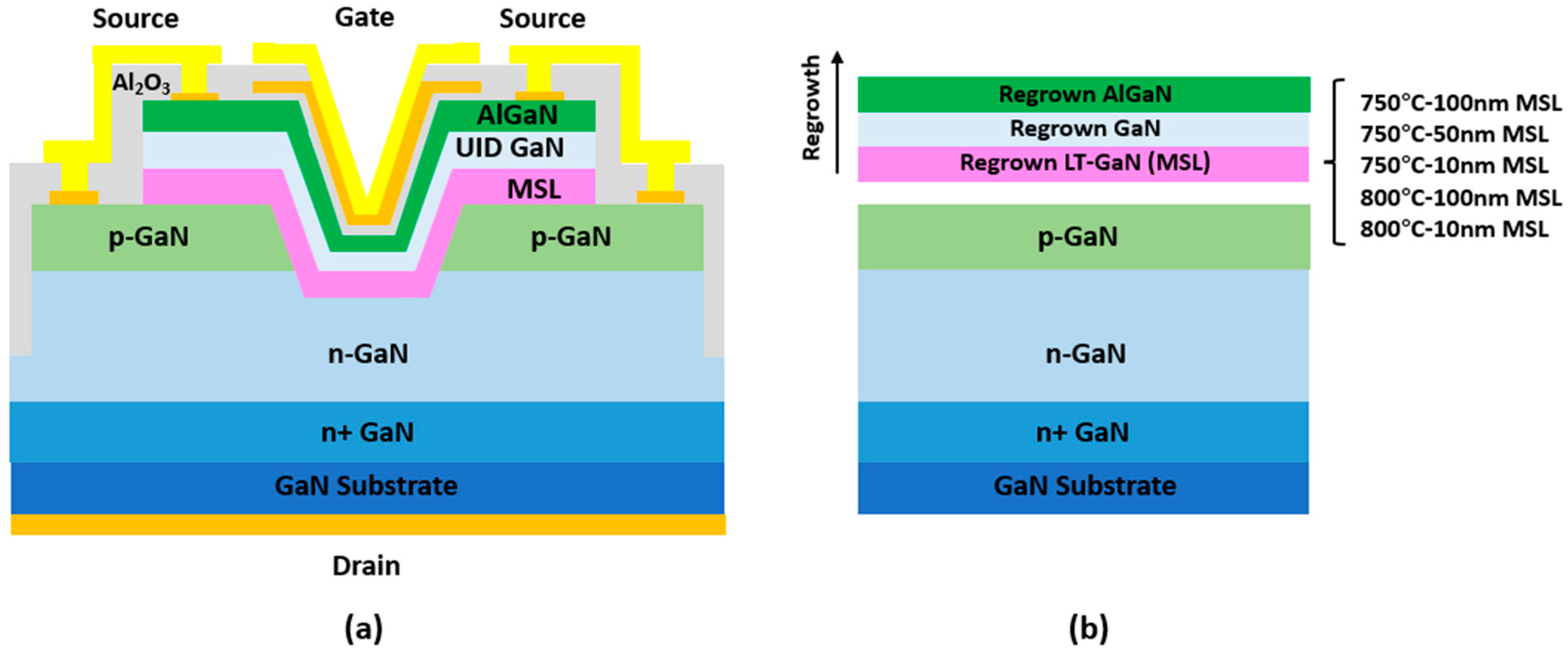
In this work, we focus on the aspect of achieving high on-state current density using an all-MOCVD process, overcoming the various challenges that the device structure presents. It is well known that as the growth temperature is decreasing, the crystal quality of GaN becomes worse with increased defect density. The LT-GaN MSL acts as a sacrificial layer to block Mg propagation, and its material properties also need to be guaranteed that the defect density should not cause leakage problems in the device. Trench CAVETs were designed and fabricated successfully with a LT-GaN Mg stopping layer (MSL) embedded between the p-GaN layer and the AlGaN/GaN heterostructure, which was aimed to block Mg propagation and redistribution. The schematic of the device structure is shown in
Figure 1a. The trench CAVET sits on a GaN native substrate to have low dislocation density in the bulk [
18]. A MOCVD-grown Mg-doped p-GaN layer serves as the CBL to generate a potential barrier. Selective-area p-type doping is achieved by trench etching to form the aperture region followed by regrowth. The top AlGaN/GaN HEMT structure is regrown by MOCVD to create 2DEG as the source carriers of the trench CAVET. To investigate the influence of MSL regrowth temperature and thickness on the current density level of the device, a total of five trench CAVET samples were fabricated in this experiment with different MSL conditions, as shown in
Figure 1b. Three of them had MSL regrown at 750 °C with varying film thicknesses of 10, 50, and 100 nm. The other two samples had MSL regrown at 800 °C with film thicknesses of 10 and 100 nm.
2. Experimental Procedure
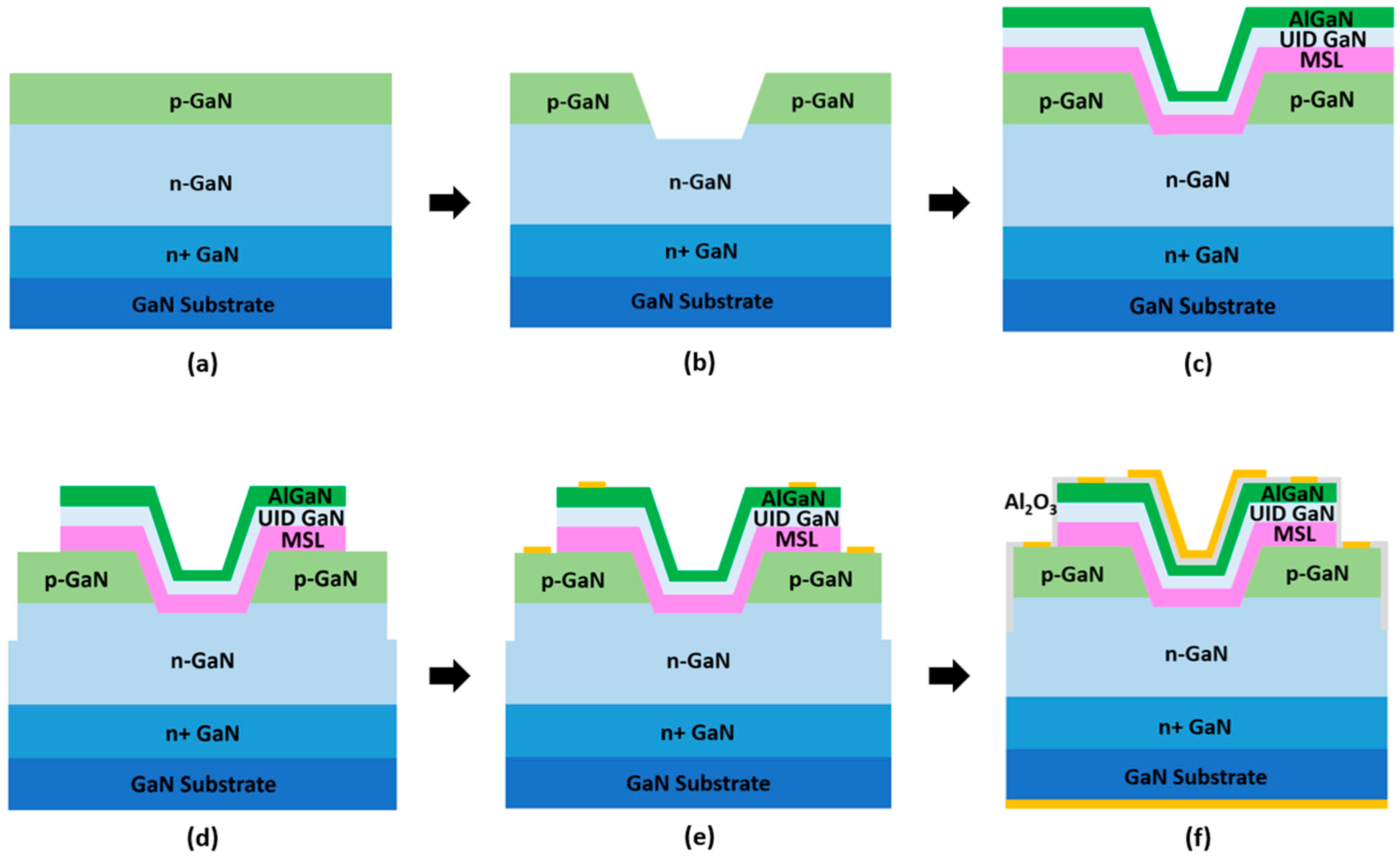
The process flow of the trench-CAVET fabrication is shown in
Figure 2. The MOCVD-grown epitaxial structure began with a 2 μm heavily doped n+ GaN layer (Si: ~1 × 10
18 cm
−3) on a homogeneous GaN substrate, followed by a 1 μm layer of n-type GaN (Si: ~1 × 10
17 cm
−3) as the drift layer. A 300 nm in-situ p-GaN layer with Mg doping density of 1 × 10
19 cm
−3 was grown on the n-type drift epitaxial layer serving as the CBL. Narrow trenches were etched using Cl
2/BCl
3 gases in inductively coupled plasma-reactive ion etching (ICP-RIE) to create the aperture regions. Tetramethylammonium hydroxide (TMAH) post-treatment was performed after aperture patterning to have a smooth surface of the trench because TMAH provides a much lower etching rate on the (
) plane of GaN than the other semi-polar planes [
19]. After a standard wafer cleaning process, regrowth to fill the trenches was conducted by MOCVD, consisting of a layer of LT-GaN that served as the MSL, a standard high-temperature 140 nm UID-GaN, and a 40 nm Al
0.3Ga
0.7N grown at 1025 °C, sequentially. Two steps of isolation etching were conducted after the MOCVD regrowth using ICP-RIE for device edge-termination. Then, the Mg dopant in the buried p-GaN layer was activated using rapid thermal annealing (RTA) at 900 °C in nitrogen (N
2) atmosphere because the atomic hydrogen incorporated into the p-GaN during growth forms Mg-H complexes, which requires high-temperature annealing to break the Mg-H bond and diffuse out hydrogen [
20]. Subsequently, a multi-layer metal stack consisting of Ti/Al/Ni/Au was deposited on the AlGaN surface as the source contact followed by a RTA annealing process at 800 °C for 45 sec to form an ohmic contact. Ni/Au metal stack on the exposed p-GaN layer formed the p-GaN contact which was later shorted to the source metal through pad connections to avoid CBL punch-through at the off-state and allow fast switching [
21]. A 12 nm gate dielectric layer of Al
2O
3 was implemented by atomic layer deposition (ALD), and then Ni/Au gate contact was patterned on top. The Ti/Au unalloyed drain contact was deposited on the backside of the substrate.
3. Results and Discussion
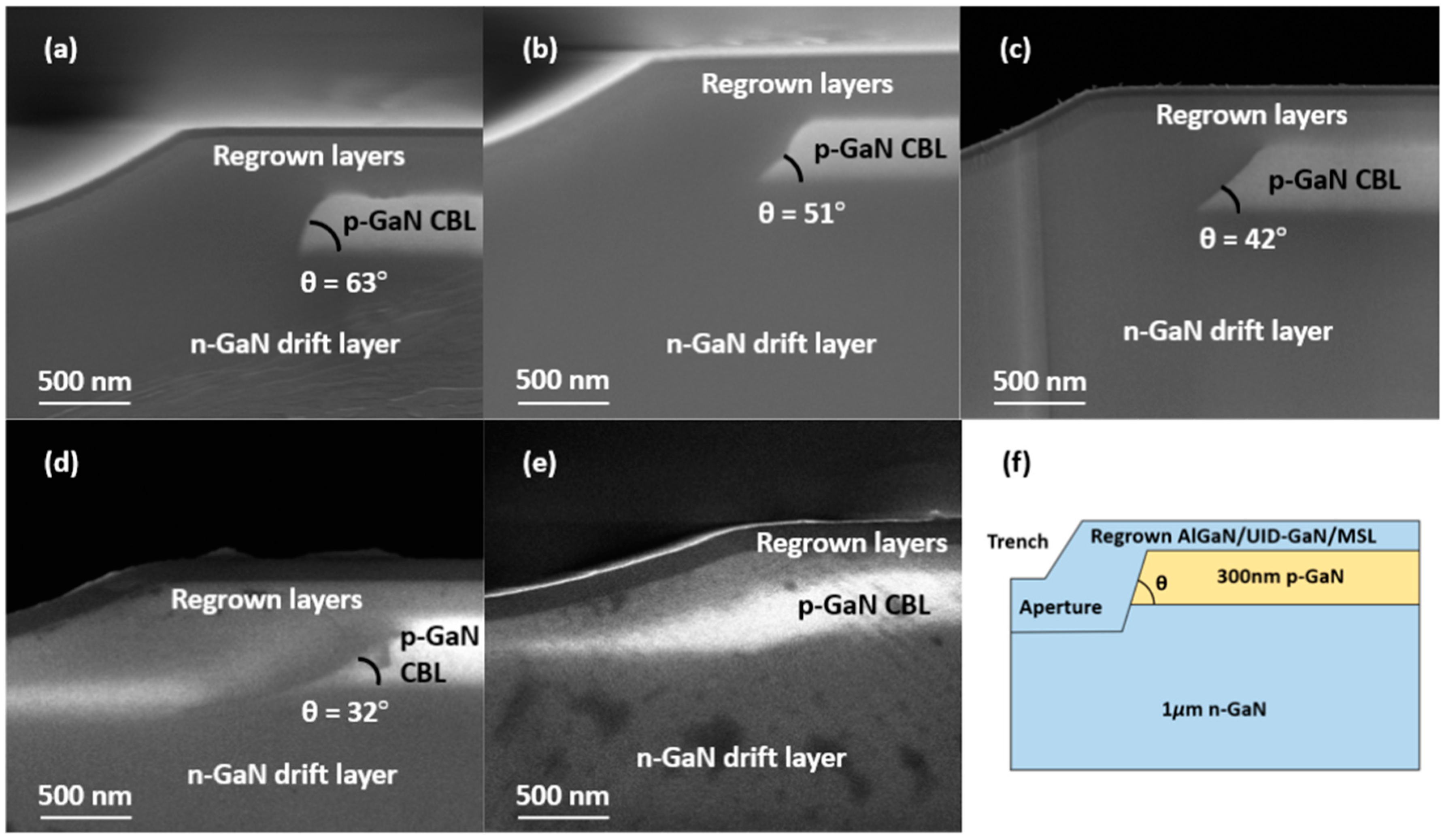
To investigate Mg propagation in the MOCVD regrown layers, cross-sections of the partial trench from the five CAVET structures were taken by scanning electron microscopy (SEM), as shown in
Figure 3. The schematic of the partial trench region is shown in
Figure 3f. The p-GaN region has the highest secondary electron emission intensity and thus appears bright in the SEM image, whereas the n-GaN regions are relatively dark [
22]. It can be clearly found from the SEM results that the regrowth thickness in the trench region was not constant, and the trench sidewalls were thicker than the basal plane due to a much faster lateral growth rate by MOCVD. The slope of the p-GaN edge, initially caused by trench etching, showed clear differences among the five trench CAVET structures with different MSL temperatures and thicknesses. Considering the MSL regrowth temperature of 750 °C, 100 nm of MSL prevented Mg out-diffusion most efficiently, presenting the steepest p-GaN slope angle (θ) of 63° and clear p-GaN boundary. θ reduced to 51° for the CAVET with 50 nm MSL and further for 10 nm MSL up to 42°. We believe that the decrease in θ originates from the lateral diffusion of Mg in p-GaN to the regrown aperture region. The top boundary of p-GaN also became more blurred with thinner MSL, which suggested more Mg incorporated into the lateral portion of the channel region above p-GaN. Increasing the regrowth temperature of MSL to 800 °C induced more significant Mg out-diffusion in the CAVETs, as shown in
Figure 3d,e. The structure with 100 nm MSL had a further decreased θ of 32°, and the aperture region became much brighter, demonstrating the spread of Mg into the aperture region. For the structure with 10 nm MSL, the white p-GaN region extended to the aperture due to a heavily increased amount of out-diffused Mg, making ambiguous territory between the p-GaN CBL and regrown layers.
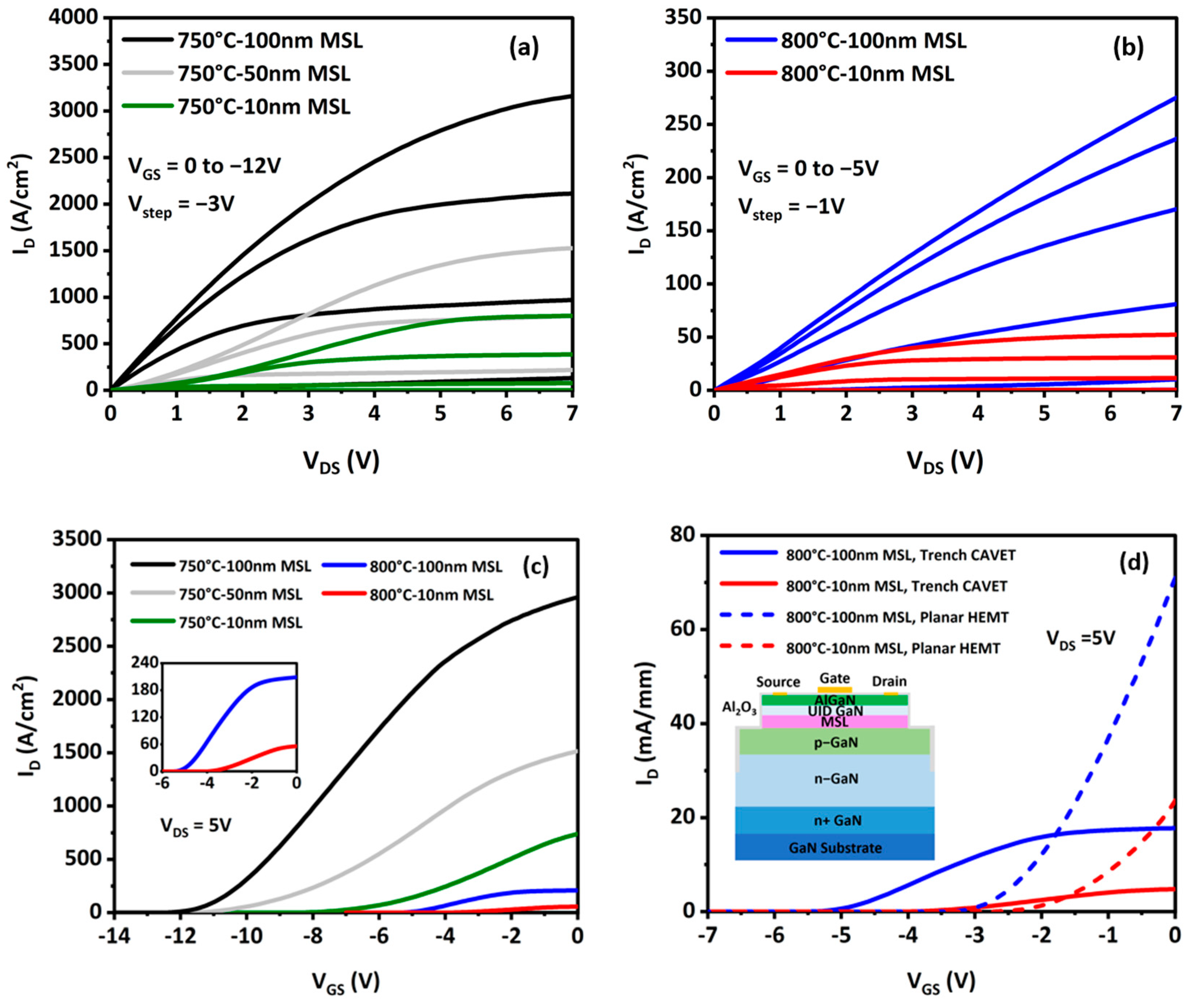
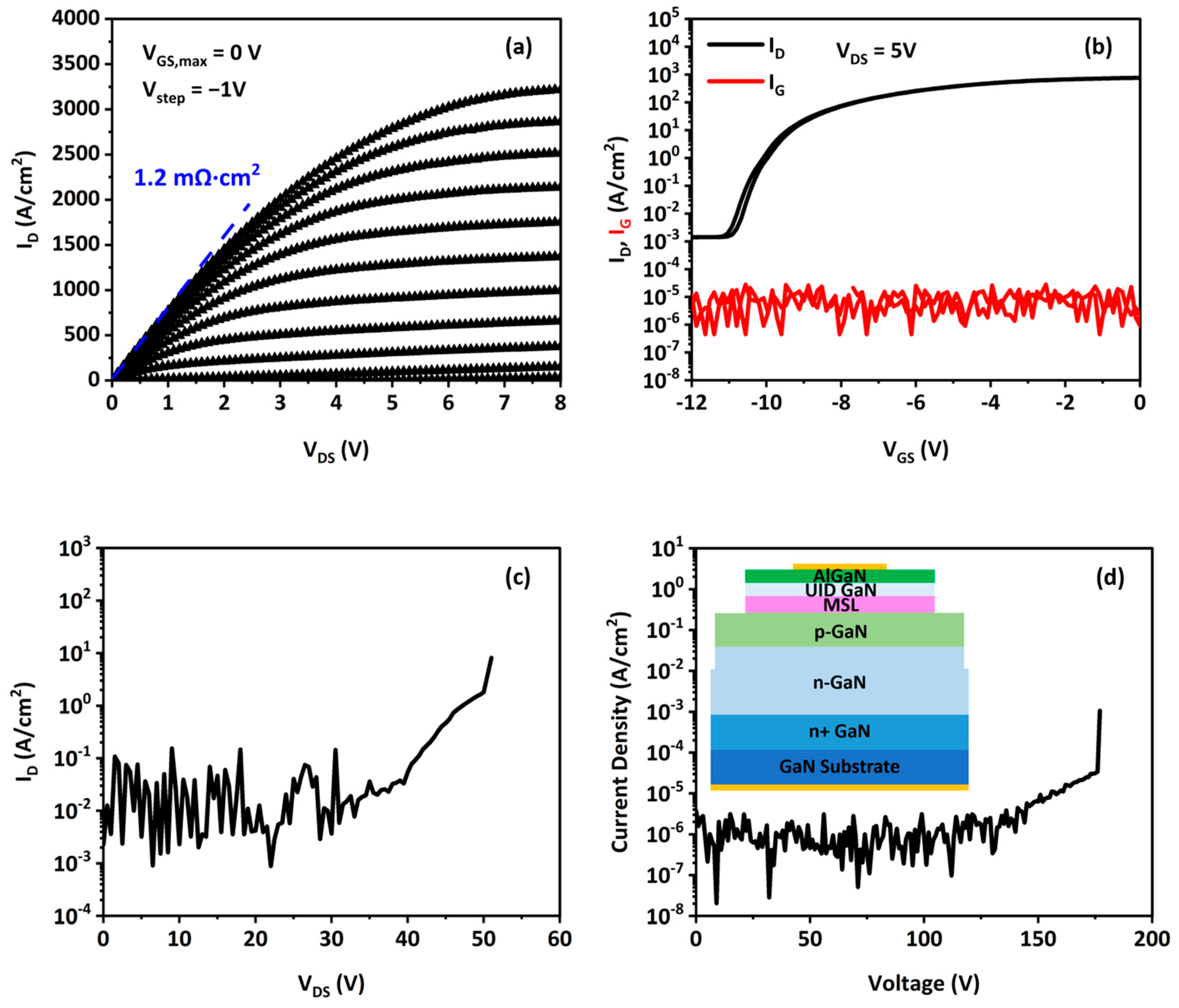
The current conductivity of the fabricated trench CAVETs was investigated to understand the impact of MSL thickness and regrowth temperature on the device electrical properties. The I
D-V
DS curves of the five CAVETs are shown in
Figure 4 a,b. Among the three trench CAVETs with MSL regrown at 750 °C, the devices with 100 nm MSL achieved the highest maximum drain current I
D,max of 3.2 kA/cm
2 (drain current density measured at V
DS = 7 V, V
GS = 0 V) and the lowest specific on-state resistance R
on,sp of 1.2 mΩ∙cm
2. The trench CAVET with 50 nm MSL showed a decrease in I
D,max to 1.5 kA/cm
2 with increased R
on,sp of 8.6 mΩ∙cm
2, and the device with 10 nm MSL had the lowest I
D,max of 800 A/cm
2 and the highest R
on,sp of 14.3 mΩ∙cm
2. For MSL grown at 800 °C, I
D,max of 275 A/cm
2 and R
on,sp of 26.4 mΩ∙cm
2 were observed for the trench CAVET with 100 nm MSL, and I
D,max of 52 A/cm
2 and R
on,sp of 70.2 mΩ∙cm
2 for the trench CAVET with 10 nm MSL. The I
D-V
GS transfer curves of the five devices in
Figure 4c exhibit that the threshold voltage V
TH of trench CAVET shifts to less negative values with higher MSL temperature and lower MSL thickness. The results reveal that the trench CAVET with MSL regrown at 750 °C retains a much higher current density by more than 10 times compared to the 800 °C-MSL device, and current decrement by higher than 50% happens when the thickness of MSL is halved. From the results, it is believed that the upward diffusion of Mg into the regrown AlGaN/GaN channel suppresses the formation of 2DEG and thus increases the channel resistance, while the lateral diffusion of Mg into the aperture compensates for the n-type dopants and leads to higher aperture resistance. Therefore, both the upward and lateral diffusion of Mg contribute to the significant increase in the total on-resistance of trench CAVET.
To further analyze the AlGaN/GaN channel carrier concentration of the trench CAVETs with MSL grown at 800 °C, I
D-V
GS transfer curves of the non-trenched CAVET structures as planar HEMTs are compared with trench CAVETs, as shown in
Figure 4d. The current unit of the trench CAVETs was transferred to mA/mm for better comparison with the lateral HEMT devices. The on-state drain current level generated by the planar HEMT structure was found to be more than twice that of the trench CAVET for both the cases of 100 nm and 10 nm MSLs. This is because a part of the 2DEG channel of the trench CAVET is located on the semi-polar plane of the slanted trench sidewalls, and thus the total polarization charge is reduced. Nonetheless, the two planar HEMTs show relatively low on-state current density, and it indicates that the 2DEG charge stored at the AlGaN/GaN interface is very limited even for the lateral portion of the regrown channel. Therefore, MSL grown at 800 °C hardly inhibits Mg propagation and leads to a substantial reduction in the channel 2DEG charge, losing the innate advantage of CAVET as a high-current-density device. Increasing the thickness of MSL is beneficial to prevent Mg out-diffusion, but it also increases the distance between the 2DEG channel and the buried p-GaN layer, and thus causes a more negative V
TH to deplete the entire thickness of the regrown GaN on top of CBL. From analyzing the I-V measurement results of the five CAVET samples, it is also worth noting that the MSL growth temperature has a more pronounced impact on the on-state current density compared to the film thickness. Therefore, considering the capability of retaining the high current density of a device, we believe that the maximum growth temperature of MSL is lower than 800 °C. However, previous studies have shown that the crystal properties of the regrown GaN layers deteriorate significantly when the MOCVD growth temperature is too low (<700 °C) [
16], which may lead to device leakage problems.
The fabricated trench CAVET with a 100 nm MSL regrown at 750 °C achieved the best device performance among the five samples.
Figure 5a shows the I
D-V
DS output characteristics of the device with gate voltage swept from 0 V to −11 V in steps of −1 V. The double-swept I
D-V
GS transfer characteristics of the device shown in
Figure 5b exhibit V
TH of −11 V and on-off ratio (I
on/I
off) of 10
6. Thanks to the high quality of the ALD Al
2O
3 gate dielectric layer, the gate leakage current density I
G is about two orders of magnitude lower than the off-state drain current density, and the clockwise hysteresis value of I
D is only 0.1 V. The off-state characteristics of the device in
Figure 5c show that the measured three-terminal breakdown voltage of the trench CAVET is 50 V sustained by a 1 μm thick drift layer with n-type doping density of ~10
17 cm
−3 by design. A thicker epitaxial drift layer with less n-type doping density can be adopted in the future to improve the breakdown voltage of the device. Additionally, the breakdown voltage of the source-to-drain n-p-n body diode was measured by applying a positive bias on the bottom electrode and ground on top, as plotted in
Figure 5d, to illustrate the blocking capability of the p-GaN CBL. A two-terminal breakdown voltage of 180 V was achieved successfully, suggesting that the buried p-GaN CBL was effectively activated by RTA with an estimated peak electric field of 3.6 MV/cm.
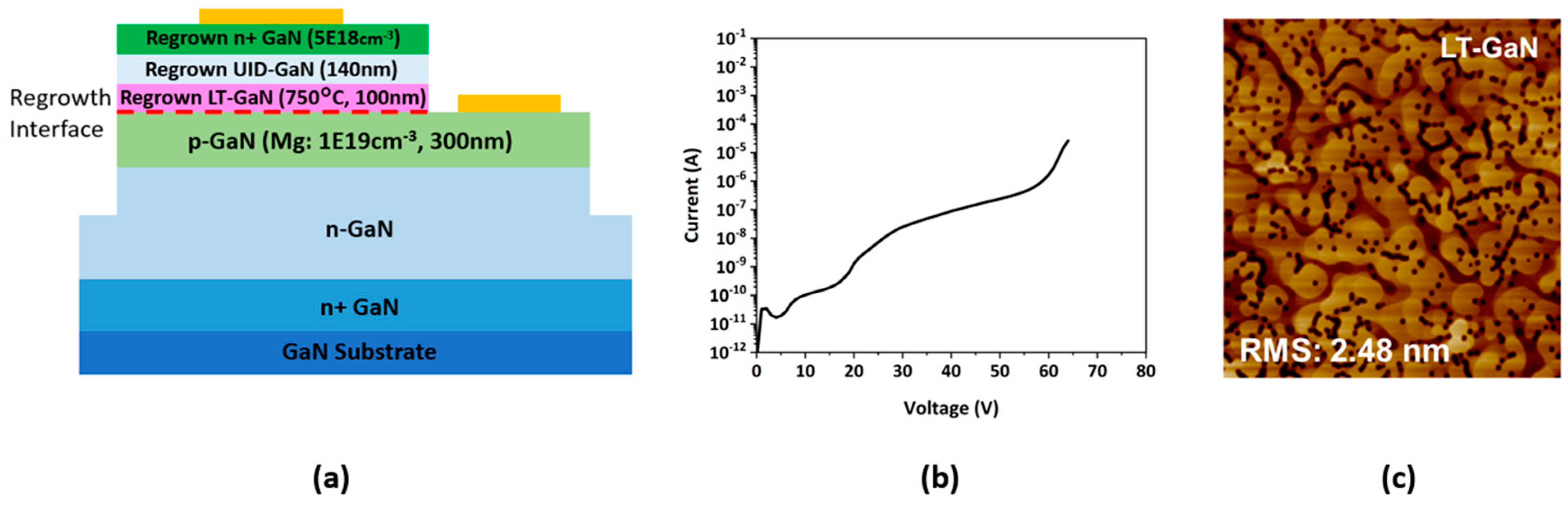
In
Figure 6, the reverse leakage current was measured from the regrown p-n junction for electrical characteristics of the regrown LT-GaN at 750 °C. The test structure shown in
Figure 6a has similar epitaxial layers of CAVET except for the regrown n+ GaN (Si: ~5 × 10
18 cm
−3) replacing the AlGaN layer. A low reverse leakage current of the isolated regrown p-n junction is displayed in
Figure 6b, which reflects that the quality of the regrown layers as well as the interface is suited for device fabrication. The atomic force microscopic (AFM) image of the regrown LT-GaN at 750 °C is shown in
Figure 6c with a root mean square (RMS) surface roughness of 2.48 nm. As a sacrificial layer, the 750 °C regrown LT-GaN effectively suppresses Mg out-diffusion and supports high current conductivity of the AlGaN/GaN heterostructure without causing severe leakage issues for device performance.
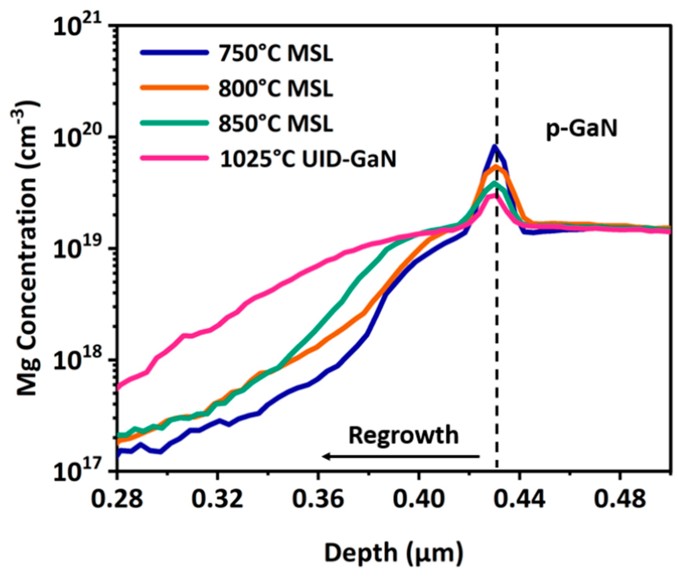
Figure 7 shows the SIMS depth profiles of four test samples with the same epitaxial layers as CAVET, three of which contained a 100 nm ex situ regrown LT-GaN layer at different temperatures (750 °C, 800 °C, and 850 °C, respectively), and a reference sample whose ex-situ regrown layer was a 100 nm high-temperature UID-GaN grown at 1025 °C, the standard temperature for GaN channel regrowth. The vertical dotted line in the figure represents a borderline to distinguish Mg residual tails in the regrown layers from Mg plateau in p-GaN CBL. The calculated decay rate of Mg tail in the UID-GaN layer regrown at 1025 °C was ~104 nm/decade, and it was decreased to ~64 nm/decade in the 850 °C-MSL, ~53 nm/decade in the 800 °C-MSL, and ~39 nm/decade in the 750 °C-MSL. Compared to high-temperature GaN regrowth at 1025 °C, the 750 °C-MSL effectively reduced the Mg diffusion decay rate by 62.5%. A narrow Mg spike was also found at the regrowth interface, and the gettering of Mg was likely due to the high defect density of the regrowth interface [
12]. Comparing the SIMS profiles at the regrowth interface of the four samples with different first regrown layers (1025 °C-, 850 °C-, 800 °C-, and 750 °C-GaN), the spike level was slightly increased with decreasing regrowth temperature, implying that a decrease in regrowth temperature may induce higher defect density at the growth interface.


