1. Introduction
Electronic illumination technology emerged in the second half of the 20th century with the advent of semiconductors. The development of efficient electroluminescence using semiconductor devices in 1962 marked a significant milestone in the creation of LED technology [
1]. Initially, LEDs were only capable of producing red light, but subsequent advancements allowed for the emission of yellow light as well. These early LEDs found their first applications in wristwatches and instrument displays, and served as indicators in instrument panels [
2,
3]. It was not until the early 1990s that LEDs capable of emitting red-to-yellow light more efficiently than incandescent lamps became widely accessible [
4].
The combination of GaN and its mixtures with InN and AlN, which are collectively known as group-III nitrides, have brought about significant changes in the solid-state lighting industry. These materials possess the ability to emit a wide range of wavelengths within the visible spectrum, making them highly desirable. Group-III-nitride-based LEDs with enhanced performance are now extensively utilized in various illumination applications, including highly efficient solid-state lighting [
5], microdisplays [
6], food processing [
7], indoor/outdoor lighting, and color displays [
8,
9]. GaN- and InGaN-based green and blue LEDs in particular demonstrate remarkable efficiency, thereby establishing themselves as crucial photonic devices [
10]. As a result of their superior efficiency and reliability compared to other lighting technologies, LEDs are experiencing a surge in popularity.
Commonly, blue LEDs are utilized for the purpose of white lighting, which is based on InGaN/GaN and is affected by a phenomenon referred to as quantum efficiency droop. This implies that when these LEDs are operated at high currents, the efficiency of converting electrical power into light diminishes. This limitation has resulted in extensive research being conducted in order to identify the underlying physical mechanisms and potential solutions. Although some researchers claim to have discovered the primary cause of this droop, uncertainty around the subject remains [
11]. The crystalline quality of the material plays a significant role in enhancing the efficiency of the conversion of electrical power into light in III-nitrides.
In the field of III-nitride materials, InGaN has attracted considerable attention as a ternary compound. GaN and InGaN, each with a high indium content, play critical roles in the production of light emitters in the visible and near-UV spectral ranges. Currently, various physical and chemical characteristics are estimated by utilizing the properties of GaN and InN, including their lattice parameters, elastic constants, band gaps (Egs), and effective electron masses. Additionally, experimental studies have revealed that the band gap of InN is less than 1.0 eV [
12,
13,
14,
15,
16]. Some researchers have relied on empirical evidence of a 1.9 eV band gap in InN to support their claims. However, it is widely accepted that the actual value of the band gap of InN is approximately 0.69 eV [
17,
18,
19]. Therefore, advancing the growth kinetics of InGaN is of the utmost importance as it has the potential to enhance the quality of InGaN films by optimizing their growth factors. Ultimately, this can pave the way for the development and production of InGaN films of superior quality [
20].
When it comes to the growth of III-V compounds, researchers encounter a range of challenges which are thoroughly discussed in this article (
Section 2). The most commonly used substrates (
Section 3) and primary growth techniques (
Section 4) are also extensively debated. Various techniques are examined to improve the EQE of InGaN, which is directly influenced by crucial parameters related to the growth temperature, V/III ratios, growth rate, and growth pressure (
Section 5). Furthermore, this article delves into the widely discussed issue of the Shockley–Read–Hall recombination lifetime (
Section 6).
Section 7 explores different recently published strategies aimed at improving the EQE of InGaN, including the implementation of a microrod crystal structure, the utilization of the piezo-phototronic effect, electron blocking, and the examination of temperature’s effect on the electron-blocking layer. To address the challenge of polarization, the concept of the piezo-phototronic effect was recently introduced as the three-way coupling of piezoelectric polarization, semiconductor properties, and optical excitation by applying the piezo-potential or piezo-charge within the semiconductor device. The quality of the crystal material may be affected by various factors, including the choice of substrate, specific growth technique, and optimized growth parameters. These factors collectively play a crucial role in determining the overall crystal quality.
2. Focused Aspects of Research on an InGaN-Based LED
Initially, the growth of InN and GaN occurs at different temperatures to achieve their optimal electronic and optical characteristics; this presents significant challenges, particularly in producing high-indium-content (In; Ga)N or (In; Ga)N/GaN heterostructures. This disparity in ideal growth temperature is due to the varying strengths of In-N and Ga-N bonds, with the former being less intense than the latter, as evidenced by the energy required to initiate the process of breakdown and removal. According to certain publications, the energy required for the decomposition of InN ranges from 1.69 eV [
21] to 1.92 eV [
22], with a desorption energy of 2.5 eV [
23]. Reports suggest that the activation energy required for the decomposition of GaN is between 3.1 eV [
24] and 3.6 eV [
25], with a desorption energy of 2.2 eV–2.8 eV [
26,
27]. The increase in the decomposition of InN becomes significant at around 480 °C according to one source [
28], whereas for GaN, it remains negligible until approximately 700 °C. However, it is worth noting that the decomposition temperatures of InN and GaN can vary depending on the pressure conditions and temperatures to which they are exposed.
The second phenomenon, referred to as the miscibility gap or phase separation, occurs across a broad spectrum of compositions and leads to inconsistencies at the nanoscale level [
29,
30,
31].
The third phenomenon involves variations in the indium content and the width of the quantum well, leading to fluctuations in the wavelength of the emitted light and the duration of radiative decay [
32,
33]. This poses a challenge in achieving the population inversion of charge carriers, which is essential for the proper functioning of LEDs [
34].
The fourth phenomenon is the significant difference in the lattice spacing between InN and GaN, which limits the maximum thickness of the InN or (In, Ga)N layer that can be grown on GaN with pseudomorphic behavior before undergoing elastic or plastic relaxation [
35,
36,
37,
38]. Furthermore, the growth of (In, Ga)N on GaN is further complicated by the presence of a phenomenon known as the composition pulling effect, which induces a compositional gradient along the direction of growth due to strain [
39,
40].
In the case of blue LEDs, although they are efficient, there is a decrease in the internal quantum efficiency caused by several factors, such as Shockley–Read–Hall recombination, auger recombination, carrier delocalization, and electron leakage [
41,
42]. Carrier concentration and temperature can have an impact on Shockley–Read–Hall recombination, auger recombination, and electron leakage.
Nevertheless, commercial LEDs grown on the c-plane of a wurtzite crystal are adversely affected by the quantum-confined Stark effect due to the significant spontaneous and piezoelectric fields associated with polarization. InGaN, with a larger lattice constant than GaN, introduces compressive strain and polarization. These strains occur at each period interface due to a mismatch between the lattice structures of InGaN and GaN. As a result, the band structure, the effective mass of electrons, the quantum well depth, and the confinement of electrons and holes in the active region are altered. This leads to a reduction in the rate of radiative recombination and a consequent increase in the lifetime of the charge carriers. Consequently, this droop in the radiative recombination rate causes a decline in the internal quantum efficiency (IQE) [
43,
44,
45].
The overall polarization is the sum of the piezoelectric caused by the deformation of the material, known as strain, and the spontaneous polarization caused by the InGaN and GaN. This polarization generates an internal electric field that counteracts the electric field applied to the LED. The applied electric field brings electrons and holes closer together for recombination but the internal electric field resulting from polarization separates them. Therefore, the internal electric field generated by polarization reduces the efficiency of the LED [
46].
3. Substrate Analysis
Some commonly used substrates for the growth of InGaN, a semiconductor material with a wide range of applications, include silicon carbide (SiC), GaN, silicon, and sapphire. These substrates play a crucial role in the epitaxial development of InGaN thin films as they provide the necessary surface and lattice structure for the material. This article will primarily focus on commonly used substrates such as silicon and sapphire, examining their unique qualities and advantages and the challenges in employing them as InGaN epitaxy substrates.
3.1. SiC
SiC substrates are frequently employed for the growth of indium gallium nitride thin films in optoelectronic device applications. The advantages and disadvantages of using SiC as a substrate for the growth of InGaN are listed. Some advantages of a SiC substrate include its wide bandgap, high levels of chemical and mechanical stability, and relatively close lattice match with InGaN, facilitating the epitaxial growth of high-quality InGaN films. However, the temperature needed for the growth of InGaN on SiC can be quite high, often surpassing 1000 °C, and SiC substrates can be more expensive than other frequently used substrates like sapphire or silicon [
47].
3.2. Gallium Nitride
InGaN films grown on GaN substrates exhibit lower dislocation densities and better optical properties compared to those grown on other substrates, which tend to have high threading dislocation densities and poor optical properties [
48]. InGaN films grown on GaN substrates have better crystal quality but they are more expensive than silicon. GaN substrates have low defect densities and high structural and optical quality [
49,
50]. The wide bandgap of GaN enables the production of InGaN layers with various tunable bandgaps, making it highly beneficial for optoelectronic devices such as light-emitting diodes (LEDs) and laser diodes. GaN also possesses high electron mobility, which refers to the rapid flow of electrons through a substance when exposed to an electric field. Additionally, it exhibits exceptional thermal conductivity and reduced on-resistance compared to conventional silicon-based devices [
51,
52].
3.3. Silicon
Si (111) is a commonly used substrate for the growth of InGaN because of its minor lattice mismatch and compatibility with InGaN. Si has a lattice constant of 5.43 Å, which is close to the lattice constant of InGaN, allowing for the high-quality epitaxial growth of InGaN on Si substrates. Furthermore, the thermal expansion coefficient of Si is similar to InGaN, which reduces the formation of defects in the epitaxial layers.
According to Wang et al. [
53], the quality of InGaN films grown on Si substrates is superior to that of films grown on other substrates in terms of structure and optical characteristics.
However, the use of GaN seed and buffer layers presents significant challenges, par-ticularly when growing GaN on silicon (Si). One of the main issues is the potential for the silicon to dissolve in the GaN layers during the growing process, resulting in the for-mation of defects and impairing the overall performance of the device. This phenomenon is known as the incorporation of silicon into GaN. During the epitaxial growth process, the diffusion of silicon into the material can introduce stacking faults, dislocations, and other crystal defects in GaN.
3.4. Sapphire
According to Ryu et al. [
54], while preparing InGaN blue LEDs, sapphire (Al
2O
3) is considered a better substrate compared to silicon (Si). If left uncontrolled, the significant lattice mismatch and the disparity in thermal expansion coefficients between GaN and silicon can result in a higher occurrence of threading dislocations.
Figure 1 shows a schematic diagram of an epitaxial structure grown on Si and a TEM image of the epitaxial layer. Multiple layers between the silicon substrate and the n-GaN layer are required for stress control to reduce dislocations. Despite this, the electroluminescence spectra of LEDs grown on silicon are broader compared to LEDs grown on sapphire. As indicated via XRD and TDD measurements, LEDs grown on sapphire are expected to be of better quality than those grown on silicon.
Figure 2 illustrates the light output power, injection current, and forward voltage (I-V), as well as external quantum efficiency values of the measured LED samples. These values are plotted against injection currents ranging up to 800 mA. Below 300 mA, the luminous outputs of both LED samples are similar.
The I-V characteristics of LEDs grown on sapphire and silicon are depicted as dotted lines in
Figure 2a. In
Figure 2b, it is evident that when the current is below 300 mA, the LED on sapphire has a higher EQE compared to the LED on silicon. The peak EQE value of the LED on silicon is 0.588, while on sapphire, it is 0.528. This observation suggests that the LED grown on sapphire is more effective than the LED grown on silicon at relatively low injection currents due to its better crystal quality, as evidenced by the XRD and TDD measurements. The Shockley–Read–Hall recombination rate of the LED grown on sapphire is lower than that of the LED grown on silicon.
In this study, the light output power and efficiency droop values of InGaN blue LEDs fabricated on silicon (111) and sapphire (c-plane) were investigated. It was concluded that the LED grown on silicon has a lower peak EQE due to its inferior crystal quality. It exhibits a better EQE at an injection current greater than 300 mA. This improvement in the EQE value of the LED grown on silicon can be attributed to its reduced efficiency droop, which is noticeably smaller compared to the LED grown on sapphire. For cost-effective products with reduced efficiency droop, silicon is preferred. However, sapphire offers higher crystal quality, greater thermal stability, and a higher peak EQE.
Table 1 shows a comprehensive and detailed analysis of the advantages and disadvantages of different substrates, namely silicon carbide, gallium nitride, silicon, and sapphire. Each substrate has distinct qualities that make it appropriate for a variety of applications while also posing unique difficulties and restrictions.
4. Main Growth Techniques
Currently, there are two predominant methods utilized for producing gallium–nitride-based structures in optoelectronic devices: metal–organic chemical vapor-phase deposition (MOCVD) and molecular beam epitaxy (MBE).
4.1. MOCVD
MOCVD is the favored method, though MBE is rapidly gaining popularity for the fabrication of single crystalline indium nitride [
55]. Generally, MOCVD boasts a higher growth rate, operates at elevated temperatures, and uses a higher concentration of precursors, enabling faster growth [
56]. Moreover, MOCVD typically yields thicker, more uniform films with fewer defects, and its equipment is less costly than the equipment required for molecular beam epitaxy. MOCVD is carried out under conditions that are close to thermodynamic equilibrium and primarily controlled by diffusion processes [
57]. It enables greater control over the growth process and is suitable for growing structures on a wider variety of substrates.
4.2. MBE
MBE provides a growth environment without hydrogen, enabling the p-type doping of GaN-based materials without a heat treatment after growth. Additionally, it significantly reduces the consumption of source materials. Furthermore, RF sources produce atomic nitrogen species that can be incorporated into the growth front regardless of the substrate temperature [
58].
Generally, the MBE growth process is mostly influenced by surface reactions between the impinging species and the outermost atomic layers. In the case of incorporating indium into the growth of InGaN via MBE, there are some similarities with MOCVD. The level of indium incorporation reduces as the substrate temperature increases [
59,
60,
61]. The source materials of Al, Ga, In, and N used during the growth process are trimethylaluminum, trimethylgallium, trimethylindium, and ammonia, respectively [
62]. A detailed comparison of the MOCVD and MBE techniques is provided in
Table 2, outlining the specific advantages, characteristics, and limitations of each method.
Consequently, the choice between the two techniques depends on the specific requirements and applications. MBE offers more precision and versatility with respect to substrate choice, while MOCVD generally exhibits a higher growth rate and produces films that are more uniform and of higher quality.
5. Preferred Synthesis Parameters
The growth of high-quality InGaN materials requires a significant amount of work due to several issues. One of the significant challenges is the difference in the inter-atomic spacing between InN and GaN, resulting in a solid phase miscibility gap [
29,
63]. Additionally, InGaN compounds tend to have low levels of indium because InN has a higher vapor pressure compared to GaN [
64]. Moreover, due to the variance in formation enthalpies between InN and GaN, the growth process leads to significant indium separation on the surface [
65]. However, these challenges can be addressed by improving the growth conditions, including utilizing lower growth temperatures, higher V/III flux ratios, lower growth rates, and lower growth pressures. In the following section, a detailed discussion is provided on how these parameters impact the growth kinetics of InGaN materials.
5.1. MOCVD Growth of Parameters
In recent studies, it was highlighted that MOCVD is widely regarded as the most prevalent and preferred technique for the growth of InGaN. In light of this, the subsequent paragraph aims to provide an in-depth analysis and comprehensive discussion of the various parameters associated with MOCVD. By delving into the intricacies of these parameters, a better understanding of the growth process and its implications can be attained.
5.1.1. Growth Temperature
The direct band gap of the semiconductor InGaN ranges from 0.7 eV (InN) to 3.4 eV (GaN) [
66]. In order to be suitable for photovoltaic applications, the active region of InGaN must have a higher proportion of indium (In). However, increasing the indium content in InGaN/GaN heterostructures is a challenging task due to difficulties related to growth parameters [
67]. It has been observed that raising the growth temperature leads to a reduction in the full width at half maximum value [
68,
69].
According to Piner et al., reducing the growth temperature from 1100 °C to 500 °C significantly reduces the amount of indium which desorbs from the surface. However, ammonia cracking is less efficient at lower temperatures, leading to a slower growth rate that could decrease the amount of indium incorporated into the film. These two factors are the consequence of the increase in the density of indium atoms that diffuse through the film surface, increasing the likelihood of creating indium clusters. Consequently, decreasing the growth temperature leads to a significant increase in the quantity of indium droplets [
70].
5.1.2. Large V/III Ratios
According to References [
71,
72], it was observed that maintaining high V/III ratios can prevent the separation of indium during the InGaN growth process. The quantity of indium on the surface reduces as the ammonia flow increases. The V/III ratio can be adjusted by changing the ammonia flow. Under a low NH
3 flow (50 sccm), a transition from two-dimensional-to-three-dimensional growth mode was observed after a few monolayers via reflection high-energy electron diffraction; however, this transition was not observed for a higher NH
3 flow (200 sccm) [
73]. The greater accessibility of nitrogen bonding sites for indium is attributed to the higher concentration of nitrogen radicals generated by ammonia, as reported in Reference [
74]. Thin heterostructures of InGaN exhibit a more significant percentage of InN and lack indium metal on their surfaces when matched to InGaN grown in bulk. It has been observed that a specific time is required to achieve the desired size of critical indium metal nuclei. If the critical time is not reached, no indium droplets are formed; instead, a higher concentration of indium atoms is present on the surface. These atoms will either evaporate or become part of the film as the top layer grows, resulting in a film with a high percentage of InN. Once the critical time is surpassed, the structure is negatively affected. In addition, the quantity of ammonia (NH
3) affects the surface morphology of InGaN. Oliver et al., observed a shift from island nucleation mode to step-flow mode as the ammonia flow rate increased. This phenomenon is thought to be caused by a decrease in the energy barrier to the incorporation of adsorbed atoms (adatoms) at the step edges [
75].
During the process of InGaN formation, it is observed that the evaporation of indium species is less pronounced at lower temperatures and higher growth rates. This phenomenon can be attributed to the trapping of indium species by the growing layer. Nevertheless, when a high-indium composition is employed, it can lead to the formation of indium droplets, phase separation, and a nonuniform composition in films. These factors collectively contribute to lower material quality, possibly due to the low surface mobility of the adatoms [
65,
76].
5.1.3. Growth Rate
According to research conducted by Strite, A.S. and H. Morkoç [
77], the quality of InGaN crystals can be significantly impacted by the speed at which they are grown. It has been found that slower growth rates lead to improved crystal quality due to lower dislocation density and better surface morphology. Additionally, a decreased growth rate can enhance the incorporation of indium, which is critical for achieving higher emission wavelengths in the blue and green regions. When reducing the growth rate, the rate of indium incorporation can be enhanced by reducing the segregation of indium atoms on the surface, allowing for the indium to be more efficiently incorporated into the InGaN lattice [
78].
A lower growth rate can also enhance the optical and crystal quality by allowing adatoms on the surface more time to reach the two-dimensional step edges of the growth front [
79]. According to Xu et al. [
80], decreasing the growth rate of InGaN leads to a more organized crystal structure and higher-quality material. Furthermore, it was discovered that a lower growth rate improves optical uniformity and enhances emission intensity. Among all factors, the growth rate factor significantly influences the properties and quality of InGaN films, and refining it can lead to better material quality and optoelectronic characteristics. Generally, the growth rate for InGaN can range from 0.1 to 1 µm/h. However, it is important to note that this rate may vary depending on the experimental conditions and the objective of the fabrication process [
81].
5.1.4. Growth Pressure
The growth of InGaN films can be significantly impacted by low pressure, especially in terms of regulating the indium composition and enhancing the crystalline quality of the film. According to a study on the consequence of growth pressure on indium integration, reducing the growing pressure from 250 to 150 Torr leads to a substantial increase in the integration of indium into the InGaN film [
82]. Another research work utilized the MOCVD technique to investigate the impact of low pressure on the growth of InGaN films and discovered that reducing the reactor pressure resulted in a significant increase in the efficiency of indium integration, along with an improvement in the surface morphology of the film [
48]. The researchers attributed these effects to reductions in gas-phase reactions and surface desorption at lower pressures, thereby facilitating a more efficient incorporation of indium atoms into the growing crystal lattice.
Table 3 below provides a thorough and exact examination of the growth parameters of the MOCVD process. When employing the metal–organic chemical vapor deposition process, these growth parameters are extremely important in defining the quality, homogeneity, and characteristics of the deposited thin films.
5.2. MBE Growth Parameters
In the MBE process, materials are deposited on the heated substrate using one or more beams of molecules, ions, or atoms. The source of the beam frequently comes from an effusion cell that holds the substance in its purest elemental form. Alternately, an electron beam can be used for physical vapor deposition. It is important to control the temperature of the effusion cell to limit any unwanted variation in material flux to less than 1%. An RF plasma cell was used to provide the nitrogen needed for the formation of nitride-based crystals. In this cell, purified nitrogen is injected, and nitrogen radicals are produced via heating, using an RF generator. The plasma-assisted MBE, which involves the utilization of three chambers, is also employed for the fabrication of InGaN. This technique enables the deposition of high-quality layers of InGaN onto substrates. By utilizing a plasma source, nitrogen radicals or ions can be created, thereby enhancing the reactivity of the nitrogen species. This plasma source allows for a more controlled and efficient incorporation of nitrogen during the development phase. Furthermore, plasma-assisted MBE enables the development of InGaN films with various indium compositions, thereby allowing for the adjustment of the bandgap and emission wavelength of the resulting material. Ultimately, plasma-assisted MBE offers precise control over the growth process and effectively reduces impurities [
83,
84,
85].
When it comes to the growth of III-V materials via MBE, the V/III ratios and growth temperature are considered the most important factors and will be discussed in further detail below.
5.2.1. V/III Ratios
The V/III ratio is a crucial parameter for the growth of III-V materials as it affects the adatom mobility, surface reconstruction, and growth mode. This is because it influences the adatom mobility [
86,
87]. Adatoms with longer diffusion lengths have the ability to move more deeply across the surface, particularly when 2D thermodynamic growth conditions are achieved. This increased mobility increases the likelihood of these adatoms integrating into energetically favorable sites within the growing crystals, resulting in a smoother 2D surface. However, if these sites are not naturally favorable crystal sites, the presence of additional defects such as stacking faults and grain boundaries can lead to the development of a rough, grain-like morphology. Research has shown that growth with an In-rich V/III ratio (0.8) at 450 °C on Ga-GaN produces smoother 2D surfaces compared to N-rich growth (V/III = 1.2) [
22]. It is important to note that V/III ratios affect not only the surface morphology but also the optical and electrical properties. One drawback of group-III-rich conditions is that the accumulation of indium or gallium at the surface can lead to droplet formation [
88].
5.2.2. Growth Temperature
The substrate temperature is the most critical growth parameter that affects the mobility and diffusion length of the surface adatoms. All thermally activated processes are influenced by the growth temperature such as decomposition, desorption, and so on. For temperatures below 480 °C on group-III-polar substrates and below 580 °C on N-polar substrates, the decomposition of InN and the desorption of In can be considered negligible. Therefore, the V/III ratio can be estimated by comparing the flux ratios of indium and nitrogen. A smooth 2D surface morphology of InN was reported for MBE within a temperature range from 450 °C to 500 °C [
89,
90]. In the case of the growth of high-quality GaN via MBE, the substrate temperature lies between 700 °C and 750 °C. However, the decomposition and desorption of GaN are not considered for temperatures exceeding 750 °C [
27].
It is crucial to note that the growth parameters might change depending on the particular MBE system, apparatus, and desired film qualities. To achieve the required InGaN film attributes, such as the composition, thickness, and crystal quality, the optimization of these parameters is frequently carried out through experimental iterations.
To enhance the efficiency of an optoelectronic device, it is important to improve the crystal quality of the material by optimizing the synthesis process. The previous sections provided an overview of all the possible best substrates, growth techniques, and problems encountered (such as differences in growth temperature, phase separation, composition fluctuations, and the lattice mismatch between InN and GaN). Furthermore, growth parameters such as the growth temperature, V/III ratio, growth rate, and growth pressure needed to achieve a high-quality material for a higher EQE were discussed.
6. Shockley–Read–Hall Recombination Lifetime in InGaN Quantum Wells
Zhou et al. [
91] explained the mechanism of the SRH recombination lifetime. It is observed that an increase in the width of QWs causes an increment in the SRH which originates from the separation of electron–hole pairs in c-plane QWs. In addition to the width of the QW, it was noted the SRH lifetime also can be pointedly increased by increasing the number of QWs. A thick QW structure (width > 2.5 nm) [
92,
93,
94,
95] grown on a c-plane shows better efficiency than a thin wall. However, the oscillator strength in thick polar QW is reduced via polarization, which implies a substantially extended radiative lifetime of thick c-plane QWs. Consequently, the IQE is expected to exhibit droop in thick QWs. Interestingly, as the QW width increases, both the SRH recombination lifetime and the radiative lifetime increase simultaneously [
96,
97]. This implies that the ratio of the total lifetime relative to the radiative lifetime (IQE) remains constant when the QW width increases, which can help clarify the apparent discrepancy in the experimental IQE. It has been hypothesized that the carrier wave function overlap or interface defects are responsible for the well-width-dependent SRH lifetime. In addition to the association with the QW width, it is well established that the InGaN underlayer strongly influences the SRH lifetime [
98].
The incorporation of an InGaN underlayer/prelayer beneath the QW region, which is commonly used in blue LEDs, leads to a significant increase in the IQE and a dramatic decrease in the SRH recombination rate, as evidenced by research studies [
99,
100]. It must be noted that the QW and underlayer should be composed of the same material, such as InGaN. To examine the QW-width- and QW-number-dependent SRH lifetime, a temperature-dependent time-resolve photoluminescence (TD-TRPL) experiment was utilized. The samples were divided into two groups (A and B) based on the structure of the active area. Group A comprised of In
0.2Ga
0.8N quantum wells, each with a constant QW width of 2.5 nm and the numbers of QWs of two and six, while group B comprised five-fold In
0.17Ga
0.83N/GaN MQWs with varying QW widths of 2.1, 3.1, and 4.2 nm. A high-resolution X-ray diffractometer (HRXRD) analysis of the sample structure revealed that all of the samples had the intended indium compositions. The data collected from the two-QW and six-QW samples in Group A were used to generate
Figure 3, which shows examples of the temperature-dependent photoluminescence (TDPL) spectra and time-resolved decay curves.
Figure 3c,d demonstrate the behavior of intensity, which stays constant until it begins to fall, indicating a steady-state condition. The black dashed line in
Figure 3c represents the lifetime extraction achieved by using a single-exponential fitting from the steady-state intensity to the 1/e of the steady-state intensity. Radiative and nonradiative recombination processes compete with one another, as seen by the temperature-related behavior in
Figure 3. The study of each of them offers a self-consistent means of distinguishing various recombination channels once the PL intensity and the effective lifetime are retrieved from the PL spectrum and the TRPL decay curve, correspondingly. The radiative lifetime
and nonradiative lifetime
comprise the effective lifetime
of the surplus carriers from the TRPL experiment, which is expressed as follows:
The temperature-dependent effective lifetime, radiative lifetime, nonradiative lifetime, and relative IQE are shown in
Figure 4 for the samples in Group A with two and six QWs, respectively. As the temperature increases, the nonradiative lifetime will decrease in a manner comparable to the IQEs. The nonradiative lifetime for the two-QW sample with low efficiency approaches the effective lifetime at room temperature, suggesting that the nonradiative process becomes dominant. This observation is consistent with the low radiative efficiency. As the bimolecular recombination lifetime is inversely proportional to the carrier density, the long radiative lifetimes observed in the experiment are the result of the low excitation used. The radiative lifetime reaches 300 ns for the two-QW sample and 650 ns for the six-QW sample at room temperature. These results suggest that increments in both the QW number and QW width are the reasons for the nonradiative lifetime increment, but the electron–hole separation could not explain the dependence on the QW number. The compensatory effect of the indium atoms, which lowers the density of the SRH centers in the top layer, was linked to the two sets of dependencies. The hypothesis that the source of SRH recombination is the same for both groups of samples is supported by the same activation energies.
7. Strategies for EQE Enhancement
7.1. Microrod Crystal Structure Approach
LEDs based on planar heterostructures have established themselves as important standards for solid-state lighting. However, the polarization field associated with the wurtzite structure possesses a notable drawback that affects the recombination of electrons and holes. In recent years, active research was conducted on InGaN microrods as potential alternatives to LEDs [
101,
102,
103,
104]. The distinctive three-dimensional structures of these microrods hold promise for a variety of applications in the field of GaN-based LEDs, including the development of flexible white LEDs [
105], single-photon sources [
106], and high-frequency LEDs [
103,
107]. One of the key advantages of using microrods in LEDs is their high surface-to-volume ratio, which results in a larger area for light output compared to chips of the same size [
108]. Additionally, the small size of the structure decreases the probability of defects, while the three-dimensional configuration enables access to various crystal facets [
109]. In InGaN/GaN heterostructures, the wurtzite lattice produces spontaneous and piezoelectric polarization that varies with the crystal facet due to crystal anisotropy.
The polarization-induced electric field in this context gives rise to the quantum confined Stark effect, resulting in a bending of the band structure within the active region [
110,
111]. This bending leads to a decrease in the overlap between the wave functions of the electrons and holes, subsequently reducing the rate of radiative recombination and increasing the lifetimes of the charge carriers [
112]. The electric field plays a particularly significant role in the direction perpendicular to the growth plane, referred to as the c-direction, which is typically the preferred growth direction for planar InGaN/GaN LEDs [
113]. However, microrod LEDs have a different dominant facet, the m-plane, which is a nonpolar plane that lacks the quantum-confined Stark effect. Despite this, the m-plane offers advantages, such as a higher modulation speed and reduced operating currents, compared to planar LEDs.
Figure 5a shows the wall-plug efficiency and the EQE of a device. The device has a maximum wall-plug efficiency of 1.5% at 30 A/cm
2, while the maximum EQE is equal to 3% at 40 A/cm
2. The EQE varies with the current density, with a maximum value of 8.3% at 260 A/cm
2 [
102]. Moreover, it has been suggested that microrod LEDs exhibit higher internal quantum efficiencies (IQEs) when grown on the nonpolar m-plane rather than the polar c-plane, as shown in
Figure 5a.
7.2. Deposition of AlN/Al2O3 Layer
Kim et al. [
114] reported that the efficiency of an InGaN blue LED was improved via the deposition of a multifunctional, ultrathin layer of AlN/Al
2O
3 on top of the P-GaN, as shown in
Figure 5b. The main obstacle to achieving high-efficiency LEDs is the low injection rate from the p-type hole transport layer (p-Gan: Mg) due to the deficient activation of the p-type dopant. This deficiency in hole injection leads to an imbalance in the numbers of holes and electrons, resulting in lower efficiency at high current densities. Another significant challenge is the polarization issue observed in InGaN/GaN LEDs grown on a c-plane using a sapphire substrate, which induces a polarization field due to lattice mismatch between the active InGaN and the underlying GaN layers. It results in bent energy bands within the InGaN/GaN multi-quantum wells, which is important for decreasing radiative recombination rates, known as the quantum-confined Stark effect [
111,
115,
116,
117,
118,
119]. Attempt to address this issue have been made using several methods, such as using nonpolar or semipolar substrates, polar MQWs with huge wave function overlap, and using an electron-blocking layer, tunneling layer, different substrates, a polarization-matched epi-layer, top surface modification, and a one-dimensional vertical structure array [
120,
121,
122,
123,
124,
125,
126]. Among these approaches, the deposition of an AlN/Al
2O
3 layer on top of InGaN/GaN showed significant improvement. The AlN/Al
2O
3 layer serves three important functions: (1) it acts as a passivation layer, reducing surface imperfections on the p-GaN and minimizing current leak and oxidation; (2) it increases the surface potential of the p-GaN, thereby improving the rate of hole injection into the MQW and reducing hole recombination at the surface; and (3) it suppresses the quantum-confined Stark effect through a band-filling effect in the MQW. These factors enhance the radiative recombination rate of electron–hole pairs and subsequently improve the light emission efficiency of InGaN/GaN LEDs. As a result, the EQE (external quantum efficiency) increased by 29% while the efficiency droop rates were reduced by up to 6% [
114].
7.3. Optimizing Performances via the Piezo-Phototronic Effect
Jiang et al. [
127] suggested that the optical properties of optoelectronic devices can be highly enhanced by using the concept of the piezo-phototronic effect. In InGaN devices, internal piezoelectric polarization causes energy bands to tilt, resulting in a reduction in the overlap of electron–hole functions and less efficient recombination. The separated InGaN/GaN single-quantum-well heterostructure membranes exhibit relaxation of internal strain and polarization compared to the as-grown sample (growth on the c-plane). To address this, the piezo-phototronic effect is introduced to remove internal strains. Firstly, photoluminescence increases by 310% under −1.05% compressive strains and then decreases by 1700% under −1.55% compressive strains. On the other hand, it decreases by 510% under +1.4% tensile strains. Previous studies utilized various techniques to reduce/modulate internal polarization, including the use of a nonpolar substrate [
128], tailoring the band energy structure [
129,
130,
131], and inverting the growth sequence [
132]. Jiang et al. [
127] used the electrochemical etching technique and explained the photoluminescence and wavelength characteristics of single-quantum-well InGaN/GaN heterostructure membranes at room temperature by applying compressive and tensile strains, as shown in
Figure 6a,b.
The photoluminescence intensity at 429 nm initially increases with the application of compressive strains but decreases with tensile strains. The intensity difference in the photoluminescence between the as-grown (strained) and released (strain-free) samples is shown in
Figure 6c. These results can be attributed to the coupling of the intrinsic polarizations and external-strain-induced polarization within the single-quantum-well InGaN/GaN heterostructure membranes. Therefore, the piezo-phototronic effect plays an important role in modifying the polarization within the sample. By effectively modifying the optoelectronic functions of charge carriers like generation, transport, and recombination, the piezo-phototronic effect couples the semiconductor properties, piezoelectric polarization, and optical excitation [
67,
133,
134], thereby enhancing device efficiency.
Lin et al. [
135] improved the efficiency of LEDs and photodetectors by utilizing the piezo-phototronic effect and forming an InGaN/GaN quantum-well membrane. They used an electrochemical etching technique with a sapphire-based-nitride epitaxial film to create InGaN. External straining was applied to optimize the emission intensity and polarization characteristics of vertical devices. A 2.04% tensile strain resulted in an increase of 183% in the relative electroluminescence intensity of the LEDs, as shown in
Figure 7. The piezo-phototronic effect induced by the external strain enhanced carrier recombination, leading to this improvement. The polarization ratio of the photo-response current in PD working mode is affected by both tensile and compressive strains. Specifically, a 107% increase in the polarization ratio is observed with 2.04% tensile strain, while an 81% reduction is observed under compressive strain. Adjustments to the anisotropic optoelectronic properties of InGaN/GaN QWs are thought to result in these changes in polarization characteristics in vertical devices. Piezoelectric polarizations and charges can be generated in semiconductor materials when subjected to external deformation, and this property, known as the piezo-phototronic effect, is applied to control the transportation of charge carriers at local junctions or contacts between different materials.
Moreover, previous research demonstrated that the piezo-phototronic effect can be achieved by applying piezoelectric charges or potentials to semiconductor devices. This effect involves the coupling of piezoelectric polarization, semiconductor properties, and optical excitation [
136,
137]. These properties were used to improve the performance of GaN-based devices [
129,
138,
139]. Research findings show that polarized lighting can significantly decrease glare [
140], alleviate eye strain, and decrease visual tension [
141].
Sha et al. [
142] demonstrated the lift-off technique, using the piezo-phototronic effect to transfer InGaN/GaN MQWs on a flexible substrate to a rigid, conventional substrate. This transfer enabled the manipulation of strains, which can influence the performance of the device. The transferred film was found to be undamaged following examinations via atomic force microscopy and high-resolution X-ray diffraction. Fabric-based wearable devices have revolutionized the field by replacing inflexible electronics with flexible, elastic, lightweight, and soft alternatives. Recent advancements in flexible electronics have shown that semiconductors have ultrathin, flexible characteristics [
143,
144]. Typically, III-V materials are grown on Si and Al
2O
3 substrates. The growth of heterojunctions in the c-direction yields the polar plane within the wurtzite structure [
145,
146]. Strains arising from thermal and lattice mismatches in the epitaxial substrate lead to strong polarization [
147]. Consequently, achieving high-performance LEDs becomes challenging due to the quantum-confinement Stark effect. This research article addresses these challenges through the utilization of the wet-etching lift-off technique, which minimizes damage to the flexible substrate. The piezo-phototronic effect is employed to investigate bending curvatures, strain conditions, and photoluminescence. By increasing the film curvature from 0 to 6.25 mm
−1, a device’s photoluminescence intensity is improved by 10%.
7.4. The Role of the Electron-Blocking Layer
Velpula et al. [
148] indicated that the main reasons for the efficiency droop in LEDs are a large overflow of electrons from the active region into the active region and insufficient hole injection into the active region. Previous studies addressed this problem by introducing p-type AlGaN as an electron-blocking layer (EBL) to prevent electron leakage [
42,
149]. Further improvements were also made to the EBL, such as the use of a double-sided AlGaN/GaN superlattice lattice-matched InAlN [
150], an InGaN/InGaN SL [
151], and EBL-free InGaN/GaN LEDs [
152] to improve the hole-injection carrier and lower electron leakage.
It was observed that the formation of an EBL can reduce electron leakage and improve hole injection in the active region, induced via the positive polarization sheet at the last quantum barrier interface [
153]. Moreover, the majority of charge carriers are likely confined and undergo radioactive recombination in the last quantum well just prior to the last QB (quantum barrier) of III-nitride-based multi-QW LEDs [
154]. Velpula et al. [
148] utilized a novel AlGaN QB as a lattice-matched EBL used instead of a conventional GaN QB. The positive sheet charges at the last QB/EBL can be eliminated due to lattice-matched conditions at this interface. Two LED structures were prepared: LED-I (GaN last QB) and LED-II (AlGaN QB). It can be noted that the internal quantum efficiency, power, and current of LED-II are better than those of LED-I. LED-I has an IQE of 91.1% at 3.5 mA, while LED-II demonstrates an IQE of 95.81% at the same current injection. However, the IQE of LED-II keeps increasing and shows an IQE of 96.11% at 150 mA, which is ~2.49 higher than that of LED-I.
7.5. The Effect of Temperature on EBL
Onwukaeme et al. [
155] studied the temperature dependence of the electron leakage current in the AlGaN EBL blue LED structure of InGaN/GaN. It was recently noted that the internal quantum efficiency value is higher at low current densities but as the current densities increase, the IQE decreases significantly [
156,
157,
158,
159,
160]. This phenomenon, known as current droop, causes thermal efficiency droop. Thermal efficiency droop has received a significant amount of attention for its uses in higher-power applications with higher thermal stabilities. Increasing the temperature contributes to the increment in nonradioactive recombination, while decreasing the radioactive recombination is the main reason for thermal efficiency droop [
161,
162,
163,
164,
165]. A recent study showed that an increase in temperature caused increases in Shockley–Read–Hall recombination and auger recombination. Electron leakage from the MQW active region of an InGaN blue LED plays a significant role in thermal efficiency droop. To address this issue, a large-band-gap material is typically injected between the MWQs and p-type GaN layer to overcome electron leakage. However, it is also expected that due to thermionic emission, electron leakage is increased with an increase in temperature [
166,
167]. Onwukaeme et al. [
155] experimentally and theoretically investigated the electron leakage characteristic in a range of temperatures from 20 °C to 100 °C, using the ABC recombination model. In
Figure 8, it can be seen that decreasing the temperature and increasing the injection current caused a significant increase in electron leakage. However, contrary to common concepts,
Figure 8 also shows that increasing the temperature caused a decrease in the electron leakage current. This reduction in electron leakage is credited to an increase in the potential barrier due to an increase in the concentration of ionized magnesium (Mg) acceptors in the EBL of AlGaN with the temperature increment.
7.6. Analysis of Conventional and Inverted LED Structures
Yadav et al. [
168] performed a comparative study to analyze the performances of LEDs with conventional (p-GaN/QW/i-GaN/n-GaN/Substrate) and inverted (n-GaN/QW/i-GaN/p-GaN/Substrate) configurations. The QW-based inverted junction and traditional LEDs display nonlinear rectifying current–voltage characteristics, with forward threshold voltages of around 0.7 V and 0.5 V, respectively. Electroluminescence was observed in both conventional and inverted junction LEDs as the injection current increased at room temperature. Additionally, LEDs with five QW periods exhibited a stronger external quantum efficiency [
169] and a carrier localization effect when compared to LEDs with different configurations at a constant injection current. It was reported that an InGaN thickness of 7.8 nm with indium doping greater than 10% showed maximum charge confinement [
170]. It was discovered that the emission from a manufactured QW LED exhibited a spectral blue shift with an increasing injection current. Conventional LEDs (topmost layer: p-type GaN) showed better luminous efficiency (2.83 lm/W) compared to inverted LEDs (1.56 lm/W; topmost layer: n-type GaN). In a normal LED device, efficiency droop was observed at 14%, but it was only 8% in the inverted LED structure.
Figure 9 shows the room-temperature photoluminescence of a thin film containing InGaN/GaN MQW. Three emission peaks at 361.1 nm, 423.8 nm, and 538.6 nm are visible in the emission spectra for the produced InGaN/GaN MQW structures. The near-band-edge (NBE) emission in the GaN film is detected at 361.10 nm [
171]. The NBE emission from the InGaN film is responsible for the appearance of another strong emission at a longer wavelength, specifically 423.8 nm [
172]. As a result, the emission in the visible range (violet-blue region) changes when an InGaN film is present in the heterostructure. The mid-gap defect states in the InGaN/GaN MQW sample can be attributed to the wider emission area at a longer wavelength (>500 nm) [
173].
The RT-electroluminescence spectra of LED structures with various numbers of InGaN/GaN quantum wells are displayed in
Figure 10. In comparison to samples with fewer QWs such as five QWs at a constant injection current of 10 mA, the sample with six displays a higher degree of leakage. In accordance with the photoluminescence spectra, the LED structure with five quantum wells exhibits a strong emission intensity peak at an injection current of 30 mA at a wavelength of 424 nm [
174].
EL intensity values versus wavelength spectra were acquired at various injection currents ranging from 10 mA to 60 mA during an RT-EL investigation on InGaN/GaN QW-based LEDs.
Figure 11a shows the result for conventional LEDs, while
Figure 11b presents the date for inverted p-i-n junction LEDs. The InGaN energy states at 425 nm, which increase with an increase in the injection current, generate a large peak which forms in the visible spectral area. Because of these current energy states of the InGaN, radiative transitions take place [
169]. At a wavelength of around 425 nm, the spatial changes in the indium composition result in this wide visible spectrum, which generates local minima in the conduction and valence bands. Indium surface segregation occurs when ternary semiconductors evolve. The radiative recombination efficiencies of InGaN/GaN QWs generated via the MBE or MOCVD techniques are affected by carrier localization in indium nitride QDs with indium contents greater than 10%. The EL intensity increases with an increase in the injection current from 10 to 60 mA. Because the undoped and n-doped GaN layers have higher carrier concentrations compared to the p-doped GaN layer, the injection of an electron from Si: GaN to Mg: GaN is visible in the EL spectrum.
The output power versus injected current density curve for the inverted LED in
Figure 12a has a threshold of 30 mA. This is because carriers migrate inside the surface of the p-n junction even if they diffuse into the QWs when the injection current is less than 30 mA [
154]. Consequently, due to the recombination of holes with the defect states, the emission intensity is low. Conventional p-i-n power can be boosted by injecting a current of up to 18.3 mW, and it can still produce a significant amount of light at low current levels. This is exemplified in
Figure 12a; a conventional LED provides more power compared to an inverted LED. EQE vs. injected current density curves for traditional and inverted blue LEDs are illustrated in
Figure 12b. The EQE of the conventional p-i-n LED increases as more current is introduced into the system, and it then slightly decreases afterwards as the current increases. Both regular and inverted LEDs experience an efficiency decline.
The applied electric field in the forward bias crosses the MQWs perpendicularly in an inverted p-i-n. The radiative recombination occurs close to the Mg: GaN layer because the holes have a short diffusion length. An injection current density of 8.1 A/cm2 causes a dramatic increase in the EQE in the standard p-i-n LED, which is followed by a droop as the current density increases to 60 A/cm2. The normal p-i-n junction LED has a greater EQE than the inverted p-i-n junction LED. The efficiency droop values are determined to be 14% and 8% for conventional and inverted p-i-n LEDs, respectively.
8. Conclusions
Possible problems such as lattice mismatch that induce defects in the crystal, phase separation, material composition, polarity, and growth challenges play important roles in upgrading the external quantum efficiency of an optoelectronic device. Key parameters including the growth temperature, V/III ratios, growth rate, and pressure must be considered carefully for the growth of high-quality InGaN. The use of sapphire substrates is preferred over silicon for better crystal quality. By changing the current density from 40 A/cm2 to 260 A/cm2 in the microrod crystal structure, the external quantum efficiency of the device increased from 3% to 8.3%. The peak EQE of an InGaN blue LED can be improved by 29% with the deposition of a multifunctional, ultrathin layer of AlN/Al2O3 on top of the P-GaN, and its efficiency droop rate can decrease by 6%. At current levels below 300 mA, the luminous outputs of both LED samples are similar, but the LED grown on sapphire has a higher EQE than the LED grown on silicon. The peak EQE value of the LED grown on silicon was 0.588, and it is 0.528 on sapphire. Conventional and inverted structures exhibit different EQE trends when subjected to higher currents. In the conventional structure, the EQE increases as a larger current is introduced, with an efficiency droop of 14%. Conversely, the EQE of an inverted structure decreases as a larger current is introduced, with an efficiency droop of 18%. One of the most commonly discussed problems in LEDs is Shockley–Read–Hall recombination. It was observed that increasing the width of QWs leads to an SRH increment which originates from the separation of electron–hole pairs in c-plane QWs. In addition to the width of QWs, it was noted the SRH lifetime is also significantly increased by increasing the number of QWs.
Based on specific needs, requirements, and applications, each MBE and MOCVD process has its benefits and suitability. MBE is known for its precision and versatility, particularly with respect to the choice of substrate. On the other hand, MOCVD typically offers a higher growth rate and produces uniform and higher-quality films. Therefore, the choice between MBE and MOCVD techniques depends on the specific requirements of the project and its desired outcomes.
The main problem with InGaN is piezoelectric polarization, which is the leading cause of the external quantum efficiency droop in InGaN devices. The summary of these papers reveals that a device grown on the m-plane has a better external quantum efficiency than a device grown on the c-plane, which yields the polar plane of the wurtzite structure. Strains in LEDs lead to polarization, and QCSE then is caused by strong internal polarization, which poses significant challenges to improving the efficiency of LEDs. The piezo-photonic effect, which is induced by external strain, can be a novel mechanism for improving the efficiency of an LED. Furthermore, it can also enhance the optical properties of the device. A tensile strain of 2.04% results in a 183% increase in the relative electroluminescence intensity of an LED. A device grown on the m-plane has a better external quantum efficiency than a device grown on the c-plane.
Author Contributions
Conceptualization, N.J. and J.J.; methodology, N.J. and J.J.; software, N.J., M.Q. and H.L.; validation, N.J., J.J. and H.Z.; formal analysis, N.J. and M.Q.; investigation, N.J. and J.J.; resources, J.J.,H.Z. and N.J.; data curation, N.J. and M.Q.; writing—original draft preparation, N.J. and J.J.; writing—review and editing, J.J., N.J. and M.Q.; visualization, J.J., N.J. and M.Q.; supervision, J.J.; project administration, N.J. and J.J.; funding acquisition, J.J. All authors have read and agreed to the published version of the manuscript.
Funding
This research was partially supported by the China Scholarship Council.
Institutional Review Board Statement
Not applicable.
Informed Consent Statement
Not applicable.
Data Availability Statement
Not applicable.
Conflicts of Interest
The authors declare no conflict of interest.
References
- Ponce, F.; Bour, D. Nitride-based semiconductors for blue and green light-emitting devices. Nature 1997, 386, 351–359. [Google Scholar] [CrossRef]
- Holonyak, N., Jr.; Bevacqua, S.F. Coherent (visible) light emission from Ga (As1−xPx) junctions. Appl. Phys. Lett. 1962, 1, 82–83. [Google Scholar] [CrossRef]
- Dupuis, R. An introduction to the development of the semiconductor laser. IEEE J. Quantum Electron. 1987, 23, 651–657. [Google Scholar] [CrossRef]
- Craford, M.G. LEDs challenge the incandescents. IEEE Circuits Devices Mag. 1992, 8, 24–29. [Google Scholar] [CrossRef]
- Zhou, X.; Tian, P.; Sher, C.W.; Wu, J.; Liu, H.; Liu, R.; Kuo, H.C. Growth, transfer printing and colour conversion techniques towards full-colour micro-LED display. Prog. Quantum Electron. 2020, 71, 100263. [Google Scholar] [CrossRef]
- Bui, H.Q.T.; Velpula, R.T.; Jain, B.; Aref, O.H.; Nguyen, H.D.; Lenka, T.R.; Nguyen, H.P.T. Full-color InGaN/AlGaN nanowire micro light-emitting diodes grown by molecular beam epitaxy: A promising candidate for next generation micro displays. Micromachines 2019, 10, 492. [Google Scholar] [CrossRef]
- Bhavya, M.; Hebbar, H.U. Efficacy of blue LED in microbial inactivation: Effect of photosensitization and process parameters. Int. J. Food Microbiol. 2019, 290, 296–304. [Google Scholar] [CrossRef]
- Bernardini, F.; Fiorentini, V.; Vanderbilt, D. Spontaneous polarization and piezoelectric constants of III-V nitrides. Phys. Rev. B 1997, 56, R10024. [Google Scholar] [CrossRef]
- Craford, M.G. Light-Emitting Diode Displays, in Flat-Panel Displays and CRTs; Springer: Berlin/Heidelberg, Germany, 1985; pp. 289–331. [Google Scholar]
- Pan, S.; Sun, C.; Zhou, Y.; Chen, W.; Zhang, R.; Zheng, Y. Investigation of the electroluminescence mechanism of GaN-based blue and green light-emitting diodes with junction temperature range of 120–373 K. Appl. Sci. 2020, 10, 444. [Google Scholar] [CrossRef]
- Gfroerer, T.H.; Chen, R.; Watt, G.; Liu, Z.; Zhang, Y. Impact of superlinear defect-related recombination on LED performance at low injection. J. Appl. Phys. 2019, 125, 204502. [Google Scholar] [CrossRef]
- Wu, J.; Walukiewicz, W.; Yu, K.M.; Ager Iii, J.W.; Haller, E.E.; Lu, H.; Schaff, W.J.; Saito, Y.; Nanishi, Y. Unusual properties of the fundamental band gap of InN. Appl. Phys. Lett. 2002, 80, 3967–3969. [Google Scholar] [CrossRef]
- Saito, Y.; Harima, H.; Kurimoto, E.; Yamaguchi, T.; Teraguchi, N.; Suzuki, A.; Araki, T.; Nanishi, Y. Growth Temperature Dependence of Indium Nitride Crystalline Quality Grown by RF-MBE. Phys. Status Solidi (b) 2002, 234, 796–800. [Google Scholar] [CrossRef]
- Davydov, V.Y.; Klochikhin, A.A.; Seisyan, R.P.; Emtsev, V.V.; Ivanov, S.V.; Bechstedt, F.; Furthmüller, J.; Harima, H.; Mudryi, V.A.; Aderhold, J.; et al. Absorption and emission of hexagonal InN. Evidence of narrow fundamental band gap. Phys. Status Solidi (b) 2002, 229, r1–r3. [Google Scholar] [CrossRef]
- Matsuoka, T.; Okamoto, H.; Nakao, M.; Harima, H.; Kurimoto, E. Optical bandgap energy of wurtzite InN. Appl. Phys. Lett. 2002, 81, 1246–1248. [Google Scholar] [CrossRef]
- Monemar, B.; Paskov, P.P.; Kasic, A. Optical properties of InN—The bandgap question. Superlattices Microstruct. 2005, 38, 38–56. [Google Scholar] [CrossRef]
- Guo, Q.X.; Tanaka, T.; Nishio, M.; Ogawa, H.; Pu, X.D.; Shen, W.Z. Observation of visible luminescence from indium nitride at room temperature. Appl. Phys. Lett. 2005, 86, 231913. [Google Scholar] [CrossRef]
- Pan, Y. The influence of N-vacancy on the electronic and optical properties of bulk InN nitrides. Mater. Sci. Eng. B 2021, 271, 115265. [Google Scholar] [CrossRef]
- Reilly, C.E.; Keller, S.; Nakamura, S.; DenBaars, S.P. Metalorganic chemical vapor deposition of InN quantum dots and nanostructures. Light Sci. Appl. 2021, 10, 150. [Google Scholar] [CrossRef]
- Yam, F.; Hassan, Z. InGaN: An overview of the growth kinetics, physical properties and emission mechanisms. Superlattices Microstruct. 2008, 43, 1–23. [Google Scholar] [CrossRef]
- Siekacz, M.; Sawicka, M.; Turski, H.; Cywiński, G.; Khachapuridze, A.; Perlin, P.; Suski, T.; Boćkowski, M.; Smalc-Koziorowska, J.; Kryśko, M.; et al. Optically pumped 500 nm InGaN green lasers grown by plasma-assisted molecular beam epitaxy. J. Appl. Phys. 2011, 110, 063110. [Google Scholar] [CrossRef]
- Gallinat, C.S.; Koblmüller, G.; Brown, J.S.; Speck, J.S. A growth diagram for plasma-assisted molecular beam epitaxy of In-face InN. J. Appl. Phys. 2007, 102, 064907. [Google Scholar] [CrossRef]
- Gallinat, C.S.; Koblmüller, G.; Brown, J.S.; Bernardis, S.; Speck, J.S.; Chern, G.D.; Readinger, E.D.; Shen, H.; Wraback, M. In-polar InN grown by plasma-assisted molecular beam epitaxy. Appl. Phys. Lett. 2006, 89, 032109. [Google Scholar] [CrossRef]
- Fernández-Garrido, S.; Koblmüller, G.; Calleja, E.; Speck, J.S. In situ GaN decomposition analysis by quadrupole mass spectrometry and reflection high-energy electron diffraction. J. Appl. Phys. 2008, 104, 033541. [Google Scholar] [CrossRef]
- Grandjean, N.; Massies, J.; Semond, F.; Karpov, S.Y.; Talalaev, R.A. GaN evaporation in molecular-beam epitaxy environment. Appl. Phys. Lett. 1999, 74, 1854–1856. [Google Scholar] [CrossRef]
- Guha, S.; Bojarczuk, N.; Kisker, D. Surface lifetimes of Ga and growth behavior on GaN (0001) surfaces during molecular beam epitaxy. Appl. Phys. Lett. 1996, 69, 2879–2881. [Google Scholar] [CrossRef]
- Heying, B.; Averbeck, R.; Chen, L.F.; Haus, E.; Riechert, H.; Speck, J.S. Control of GaN surface morphologies using plasma-assisted molecular beam epitaxy. J. Appl. Phys. 2000, 88, 1855–1860. [Google Scholar] [CrossRef]
- Adelmann, C.; Brault, J.; Jalabert, D.; Gentile, P.; Mariette, H.; Mula, G.; Daudin, B. Dynamically stable gallium surface coverages during plasma-assisted molecular-beam epitaxy of (0001) GaN. J. Appl. Phys. 2002, 91, 9638–9645. [Google Scholar] [CrossRef]
- Ho, I.H.; Stringfellow, G. Solid phase immiscibility in GaInN. Appl. Phys. Lett. 1996, 69, 2701–2703. [Google Scholar] [CrossRef]
- Zheng, J.; Kang, J. Theoretical study of phase separation in wurtzite InGaN. Mater. Sci. Semicond. Process. 2006, 9, 341–344. [Google Scholar] [CrossRef]
- Doppalapudi, D.; Basu, S.N.; Ludwig, K.F., Jr.; Moustakas, T.D. Phase separation and ordering in InGaN alloys grown by molecular beam epitaxy. J. Appl. Phys. 1998, 84, 1389–1395. [Google Scholar] [CrossRef]
- Gladysiewicz, M.; Kudrawiec, R. Theoretical studies of the influence of structural inhomogeneities on the radiative recombination time in polar InGaN quantum wells. Phys. Status Solidi (a) 2012, 209, 752–760. [Google Scholar] [CrossRef]
- Ponce, F.A.; Srinivasan, S.; Bell, A.; Geng, L.; Liu, R.; Stevens, M.; Cai, J.; Omiya, H.; Marui, H.; Tanaka, S. Microstructure and electronic properties of InGaN alloys. Phys. Status Solidi (b) 2003, 240, 273–284. [Google Scholar] [CrossRef]
- Holec, D.; Costa, P.; Kappers, M.; Humphreys, C. Critical thickness calculations for InGaN/GaN. J. Cryst. Growth 2007, 303, 314–317. [Google Scholar] [CrossRef]
- Zhang, J.C.; Jiang, D.S.; Sun, Q.; Wang, J.F.; Wang, Y.T.; Liu, J.P.; Chen, J.; Jin, R.Q.; Zhu, J.J.; Yang, H.; et al. Influence of dislocations on photoluminescence of InGaN/GaN multiple quantum wells. Appl. Phys. Lett. 2005, 87, 071908. [Google Scholar] [CrossRef]
- Liu, R.; Mei, J.; Srinivasan, S.; Omiya, H.; Ponce, F.A.; Cherns, D.; Narukawa, Y.; Mukai, T. Misfit dislocation generation in InGaN epilayers on free-standing GaN. Jpn. J. Appl. Phys. 2006, 45, L549. [Google Scholar] [CrossRef]
- Determination of the critical layer thickness in the InGaN/GaN heterostructures. Appl. Phys. Lett. 1999, 75, 2776–2778. [CrossRef]
- Bazioti, C.; Papadomanolaki, E.; Kehagias, T.; Walther, T.; Smalc-Koziorowska, J.; Pavlidou, E.; Komninou, P.; Karakostas, T.; Iliopoulos, E.; Dimitrakopulos, G.P. Defects, strain relaxation, and compositional grading in high indium content InGaN epilayers grown by molecular beam epitaxy. J. Appl. Phys. 2015, 118, 155301. [Google Scholar] [CrossRef]
- Hiramatsu, K.; Kawaguchi, Y.; Shimizu, M.; Sawaki, N.; Zheleva, T.; Davis, R.F.; Tsuda, H.; Taki, W.; Kuwano, N.; Oki, K. The composition pulling effect in MOVPE grown InGaN on GaN and AlGaN and its TEM characterization. MRS Internet J. Nitride Semicond. Res. 1997, 2, 11. [Google Scholar] [CrossRef]
- Lin, Y.-S.; Ma, K.-J.; Hsu, C.; Feng, S.-W.; Cheng, Y.-C.; Liao, C.-C.; Yang, C.C.; Chou, C.-C.; Lee, C.-M.; Chyi, J.-I. Dependence of composition fluctuation on indium content in InGaN/GaN multiple quantum wells. Appl. Phys. Lett. 2000, 77, 2988–2990. [Google Scholar] [CrossRef]
- Jeong, T.; Park, H.J.; Ju, J.W.; Oh, H.S.; Baek, J.H.; Ha, J.S.; Ryu, G.H.; Ryu, H.Y. High Efficiency InGaN Blue Light-Emitting Diode with >4—W Output Power at 3 A. IEEE Photonics Technol. Lett. 2014, 26, 649–652. [Google Scholar] [CrossRef]
- Verzellesi, G.; Saguatti, D.; Meneghini, M.; Bertazzi, F.; Goano, M.; Meneghesso, G.; Zanoni, E. Efficiency droop in InGaN/GaN blue light-emitting diodes: Physical mechanisms and remedies. J. Appl. Phys. 2013, 114, 071101. [Google Scholar] [CrossRef]
- Fu, H.; Lu, Z.; Zhao, X.H.; Zhang, Y.H.; DenBaars, S.P.; Nakamura, S.; Zhao, Y. Study of Low-Efficiency Droop in Semipolar (2021) InGaN Light-Emitting Diodes by Time-Resolved Photoluminescence. J. Disp. Technol. 2016, 12, 736–741. [Google Scholar] [CrossRef]
- Fiorentini, V.; Bernardini, F.; Della Sala, F.; Di Carlo, A.; Lugli, P. Effects of macroscopic polarization in III-V nitride multiple quantum wells. Phys. Rev. B 1999, 60, 8849. [Google Scholar] [CrossRef]
- David, A.; Young, N.G.; Lund, C.; Craven, M.D. The physics of recombinations in III-nitride emitters. ECS J. Solid State Sci. Technol. 2019, 9, 16021. [Google Scholar] [CrossRef]
- Anchal, N.; Sahoo, B.K. Effect of strain on internal quantum efficiency of InGaN/GaN blue LED. Mater. Today Proc. 2020, 28, 311–313. [Google Scholar] [CrossRef]
- Zhao, Y.; Xu, S.; Peng, R.; Du, J.; Fan, X.; Tao, H.; Zhang, J.; Zhang, J.; Feng, L.; Hao, Y. Performance enhancement of InGaN/GaN MQWs grown on SiC substrate with sputtered AlN nucleation layer. Mater. Lett. 2021, 294, 129783. [Google Scholar] [CrossRef]
- Lang, S.B. Guide to the Literature of Piezoelectricity and Pyroelectricity. 28. Ferroelectrics 2007, 361, 130–216. [Google Scholar] [CrossRef]
- Paskova, T.; Hanser, D.A.; Evans, K.R. GaN substrates for III-nitride devices. Proc. IEEE 2009, 98, 1324–1338. [Google Scholar] [CrossRef]
- Paskova, T.; Evans, K.R. GaN substrates—Progress, status, and prospects. IEEE J. Sel. Top. Quantum Electron. 2009, 15, 1041–1052. [Google Scholar] [CrossRef]
- Yusof, A.S.; Hamady, S.O.S.; Chevallier, C.; Fressengeas, N.; Hassan, Z.; Ng, S.S.; Ahmad, M.A.; Lim, W.F.; Seliman, M.A.C. Analysis using a two-layer model of the transport properties of InGaN epilayers grown on GaN template substrate. Mater. Sci. Semicond. Process. 2022, 144, 106614. [Google Scholar] [CrossRef]
- Liu, Z.; Nitta, S.; Robin, Y.; Kushimoto, M.; Deki, M.; Honda, Y.; Pristovsek, M.; Amano, H. Morphological study of InGaN on GaN substrate by supersaturation. J. Cryst. Growth 2019, 508, 58–65. [Google Scholar] [CrossRef]
- Wang, X.; Yu, R.; Jiang, C.; Hu, W.; Wu, W.; Ding, Y.; Peng, W.; Li, S.; Wang, Z.L. Piezotronic effect modulated heterojunction electron gas in AlGaN/AlN/GaN heterostructure microwire. Adv. Mater. 2016, 28, 7234–7242. [Google Scholar] [CrossRef] [PubMed]
- Ryu, H.Y.; Jeon, K.S.; Kang, M.G.; Yuh, H.K.; Choi, Y.H.; Lee, J.S. A comparative study of efficiency droop and internal electric field for InGaN blue lighting-emitting diodes on silicon and sapphire substrates. Sci. Rep. 2017, 7, 44814. [Google Scholar] [CrossRef] [PubMed]
- Naoi, H.; Kurouchi, M.; Muto, D.; Araki, T.; Miyajima, T.; Nanishi, Y. Growth of high-quality In-rich InGaN alloys by RF–MBE for the fabrication of InN-based quantum well structures. J. Cryst. Growth 2006, 288, 283–288. [Google Scholar] [CrossRef]
- Benzarti, Z.; Sekrafi, T.; Bougrioua, Z.; Khalfallah, A.; El Jani, B. Effect of SiN Treatment on Optical Properties of InxGa1−xN/GaN MQW Blue LEDs. J. Electron. Mater. 2017, 46, 4312–4320. [Google Scholar] [CrossRef]
- Herman, M.A.; Sitter, H.; Herman, M.A.; Sitter, H. Fundamentals of the MBE Growth Process. In Molecular Beam Epitaxy: Fundamentals and Current Status; Springer: Berlin/Heidelberg, Germany, 1989; pp. 215–277. [Google Scholar]
- Laukkanen, P.; Lehkonen, S.; Uusimaa, P.; Pessa, M.; Seppälä, A.; Ahlgren, T.; Rauhala, E. Emission studies of InGaN layers and LEDs grown by plasma-assisted MBE. J. Cryst. Growth 2001, 230, 503–506. [Google Scholar] [CrossRef]
- Chen, H.; Feenstra, R.M.; Northrup, J.E.; Neugebauer, J.; Greve, D. Indium incorporation and surface segregation during InGaN growth by molecular beam epitaxy: Experiment and theory. MRS Internet J. Nitride Semicond. Res. 2001, 6, 11. [Google Scholar] [CrossRef]
- Kushi, K.; Sasamoto, H.; Sugihara, D.; Nakamura, S.; Kikuchi, A.; Kishino, K. High speed growth of device quality GaN and InGaN by RF-MBE. Mater. Sci. Eng. B 1999, 59, 65–68. [Google Scholar] [CrossRef]
- Böttcher, T.; Einfeldt, S.; Kirchner, V.; Figge, S.; Heinke, H.; Hommel, D.; Selke, H.; Ryder, P.L. Incorporation of indium during molecular beam epitaxy of InGaN. Appl. Phys. Lett. 1998, 73, 3232–3234. [Google Scholar] [CrossRef]
- Mo, C.; Fang, W.; Pu, Y.; Liu, H.; Jiang, F. Growth and characterization of InGaN blue LED structure on Si (1 1 1) by MOCVD. J. Cryst. Growth 2005, 285, 312–317. [Google Scholar] [CrossRef]
- Pearton, S.J. GaN and Related Materials II; CRC Press: Boca Raton, FL, USA, 2000; Volume 7. [Google Scholar]
- Nagatomo, T.; Kuboyama, T.; Minamino, H.; Omoto, O. Properties of Ga1−xInxN films prepared by MOVPE. Jpn. J. Appl. Phys. 1989, 28, L1334. [Google Scholar] [CrossRef]
- Matsuoka, T.; Yoshimoto, N.; Sasaki, T.; Katsui, A. Wide-gap semiconductor InGaN and InGaAlN grown by MOVPE. J. Electron. Mater. 1992, 21, 157–163. [Google Scholar] [CrossRef]
- Mukose, K.; Sano, M. Theoretical study of composition fluctuation in InGaN films on various substrates. J. Phys. Conf. Ser. 2009, 152, 12025. [Google Scholar] [CrossRef]
- Wang, H.; Jiang, D.; Jahn, U.; Zhu, J.; Zhao, D.; Liu, Z.; Zhang, S.; Qiu, Y.; Yang, H. Investigation on the strain relaxation of InGaN layer and its effects on the InGaN structural and optical properties. Phys. B Condens. Matter 2010, 405, 4668–4672. [Google Scholar] [CrossRef]
- Surender, S.; Prabakaran, K.; Loganathan, R.; Pradeep, S.; Singh, S.; Baskar, K. Effect of growth temperature on InGaN/GaN heterostructures grown by MOCVD. J. Cryst. Growth 2017, 468, 249–251. [Google Scholar] [CrossRef]
- Piner, E.L.; McIntosh, F.G.; Roberts, J.C.; Aumer, M.E.; Joshkin, V.A.; Bedair, S.M.; El-Masry, N.A. Growth and properties of InGaN and AlInGaN thin films on (0001) sapphire. Mater. Res. Soc. Internet J. Nitride Semicond. Res. 1996, 1, e43. [Google Scholar] [CrossRef]
- Van der Stricht, W.; Moerman, I.; Demeester, P.; Considine, L.; Thrush, E.J.; Crawley, J.A. MOVPE growth optimization of high quality InGaN films. MRS Internet J. Nitride Semicond. Res. 1997, 2, 19. [Google Scholar] [CrossRef]
- Waltereit, P.; Brandt, O.; Ploog, K.H.; Tagliente, M.A.; Tapfer, L. Indium Surface Segregation during Growth of (In, Ga) N/GaN Multiple Quantum Wells by Plasma-Assisted Molecular Beam Epitaxy. Phys. Status Solidi (b) 2001, 228, 49–53. [Google Scholar] [CrossRef]
- Grandjean, N.; Damilano, B.; Massies, J. Group-III nitride quantum heterostructures grown by molecular beam epitaxy. J. Phys. Condens. Matter 2001, 13, 6945. [Google Scholar] [CrossRef]
- Oliver, R.A.; Sumner, J.; Kappers, M.J.; Humphreys, C.J. Morphological changes of InGaN epilayers during annealing assessed by spectral analysis of atomic force microscopy images. J. Appl. Phys. 2009, 106, 054319. [Google Scholar] [CrossRef]
- Keller, S.; Keller, B.P.; Kapolnek, D.; Abare, A.C.; Masui, H.; Coldren, L.A.; Mishra, U.K.; Baars, S.P.D. Growth and characterization of bulk InGaN films and quantum wells. Appl. Phys. Lett. 1996, 68, 3147–3149. [Google Scholar] [CrossRef]
- Keller, S.; Keller, B.; Kapolnek, D.; Mishra, U.; DenBaars, S.; Shmagin, I.; Kolbas, R.; Krishnankutty, S. Growth of bulk InGaN films and quantum wells by atmospheric pressure metalorganic chemical vapour deposition. J. Cryst. Growth 1997, 170, 349–352. [Google Scholar] [CrossRef]
- Keller, S.; Chichibu, S.; Minsky, M.; Hu, E.; Mishra, U.; DenBaars, S. Effect of the growth rate and the barrier doping on the morphology and the properties of InGaN/GaN quantum wells. J. Cryst. Growth 1998, 195, 258–264. [Google Scholar] [CrossRef]
- Strite, A.S.; Morkoç, H. GaN, AlN, and InN: A review. J. Vac. Sci. Technol. B Microelectron. Nanometer Struct. Process. Meas. Phenom. 1992, 10, 1237–1266. [Google Scholar] [CrossRef]
- Bo, W.; Ruolian, J.; Chengxiang, L.; Zili, X.; Jianjun, Z.; Ping, H.; Rong, Z.; Youdou, Z. Influence of Thermal Annealing on Properties of InGaN Films. J. Semicond. 2006, 27, 92–96. [Google Scholar]
- Lee, S.-N.; Sakong, T.; Lee, W.; Paek, H.; Seon, M.; Lee, I.-H.; Nam, O.; Park, Y. Characterization of optical and crystal qualities in InxGa1−xN/InyGa1−yN multi-quantum wells grown by MOCVD. J. Cryst. Growth 2003, 250, 256–261. [Google Scholar] [CrossRef]
- Xu, X.; Barrows, F.; Dravid, V.P.; Haile, S.M.; Phatak, C. Quantifying leakage fields at ionic grain boundaries using off-axis electron holography. J. Appl. Phys. 2020, 128, 214301. [Google Scholar] [CrossRef]
- Mikawa, Y.; Ishinabe, T.; Kawabata, S. Ammonothermal growth of polar and non-polar bulk GaN crystal. In Proceedings of the SPIE OPTO Gallium Nitride Materials and Devices X Conference, San Francisco, CA, USA, 7–12 February 2015; Volume 9363. [Google Scholar]
- Kim, D.-J.; Moon, Y.-T.; Song, K.-M.; Lee, I.-H.; Park, S.-J. Effect of growth pressure on indium incorporation during the growth of InGaN by MOCVD. J. Electron. Mater. 2001, 30, 99–102. [Google Scholar] [CrossRef]
- Turski, H.; Feduniewicz-Żmuda, A.; Sawicka, M.; Reszka, A.; Kowalski, B.; Kryśko, M.; Wolny, P.; Smalc-Koziorowska, J.; Siekacz, M.; Muzioł, G.; et al. Nitrogen-rich growth for device quality N-polar InGaN/GaN quantum wells by plasma-assisted MBE. J. Cryst. Growth 2019, 512, 208–212. [Google Scholar] [CrossRef]
- Siekacz, M.; Wolny, P.; Ernst, T.; Grzanka, E.; Staszczak, G.; Suski, T.; Feduniewicz-Żmuda, A.; Sawicka, M.; Moneta, J.; Anikeeva, M.; et al. Impact of the substrate lattice constant on the emission properties of InGaN/GaN short-period superlattices grown by plasma assisted MBE. Superlattices Microstruct. 2019, 133, 106209. [Google Scholar] [CrossRef]
- Lotsari, A.; Dimitrakopulos, G.; Kehagias, T.; Das, A.; Monroy, E.; Komninou, P. Structural properties of semipolar InGaN/GaN quantum dot superlattices grown by plasma-assisted MBE. Microelectron. Eng. 2012, 90, 108–111. [Google Scholar] [CrossRef]
- Gan, C.K.; Srolovitz, D.J. First-principles study of wurtzite InN (0001) and (000 1) surfaces. Phys. Rev. B 2006, 74, 115319. [Google Scholar] [CrossRef]
- Wang, X.; Che, S.-B.; Ishitani, Y.; Yoshikawa, A. Step-flow growth of In-polar InN by molecular beam epitaxy. Jpn. J. Appl. Phys. 2006, 45, L730. [Google Scholar] [CrossRef]
- Kruse, C.; Einfeldt, S.; Böttcher, T.; Hommel, D.; Rudloff, D.; Christen, J. Spatially modified layer properties related to the formation of gallium droplets on GaN (0001) surfaces during plasma-assisted molecular-beam epitaxy. Appl. Phys. Lett. 2001, 78, 3827–3829. [Google Scholar] [CrossRef]
- Yamaguchi, W.; Che, S.; Kikukawa, N.; Ishitani, Y.; Yoshikawa, A. Towards fabrication of In-polar InN films and InN/GaN MQWs. Phys. Status Solidi (c) 2006, 3, 1511–1514. [Google Scholar] [CrossRef]
- Yamaguchi, T.; Nanishi, Y. Indium droplet elimination by radical beam irradiation for reproducible and high-quality growth of InN by RF molecular beam epitaxy. Appl. Phys. Express 2009, 2, 51001. [Google Scholar] [CrossRef]
- Zhou, R.; Ikeda, M.; Zhang, F.; Liu, J.; Zhang, S.; Tian, A.; Wen, P.; Li, D.; Zhang, L.; Yang, H. Total-InGaN-thickness dependent Shockley-Read-Hall recombination lifetime in InGaN quantum wells. J. Appl. Phys. 2020, 127, 13103. [Google Scholar] [CrossRef]
- Juršėnas, S.; Miasojedovas, S.; Kurilčik, G.; Žukauskas, A.; Feng, S.; Cheng, Y.; Yang, C.C.; Kuo, C.; Tsang, J. Quantum-well thickness dependence of stimulated emission in InGaN/GaN structures. Phys. Status Solidi (c) 2003, 2610–2613. [Google Scholar] [CrossRef]
- Laubsch, A.; Sabathil, M.; Baur, J.; Peter, M.; Hahn, B. High-power and high-efficiency InGaN-based light emitters. IEEE Trans. Electron Devices 2009, 57, 79–87. [Google Scholar] [CrossRef]
- Lin, Y.W.; Wang, C.K.; Chiou, Y.Z.; Chang, H.M.; Chang, S.J. Investigation of optical and electrical properties of GaN-based blue light-emitting diodes with various quantum well thicknesses. J. Photonics Energy 2015, 5, 57612. [Google Scholar] [CrossRef]
- Zhao, K.; Yang, X.; Xu, B.; Li, D.; Wang, C.; Feng, L. Well thickness dependence of the internal quantum efficiency and carrier concentration in gan-based multiple quantum well light-emitting diodes. J. Electron. Mater. 2016, 45, 786–790. [Google Scholar]
- David, A.; Hurni, C.A.; Young, N.G.; Craven, M.D. Field-assisted Shockley-Read-Hall recombinations in III-nitride quantum wells. Appl. Phys. Lett. 2017, 111, 233501. [Google Scholar] [CrossRef]
- Zhou, R.; Ikeda, M.; Zhang, F.; Liu, J.; Zhang, S.; Tian, A.; Wen, P.; Li, D.; Zhang, L.; Yang, H. Steady-state recombination lifetimes in polar InGaN/GaN quantum wells by time-resolved photoluminescence. Jpn. J. Appl. Phys. 2019, 58, SCCB07. [Google Scholar]
- Haller, C.; Carlin, J.-F.; Jacopin, G.; Liu, W.; Martin, D.; Butté, R.; Grandjean, N. GaN surface as the source of non-radiative defects in InGaN/GaN quantum wells. Appl. Phys. Lett. 2018, 113, 111106. [Google Scholar]
- Akasaka, T.; Gotoh, H.; Saito, T.; Makimoto, T. High luminescent efficiency of InGaN multiple quantum wells grown on InGaN underlying layers. Appl. Phys. Lett. 2004, 85, 3089–3091. [Google Scholar] [CrossRef]
- Armstrong, A.M.; Bryant, B.N.; Crawford, M.H.; Koleske, D.D.; Lee, S.R.; Wierer, J.J. Defect-reduction mechanism for improving radiative efficiency in InGaN/GaN light-emitting diodes using InGaN underlayers. J. Appl. Phys. 2015, 117, 134501. [Google Scholar] [CrossRef]
- Meier, J.; Bacher, G. Progress and challenges of InGaN/GaN-based core–shell microrod LEDs. Materials 2022, 15, 1626. [Google Scholar] [CrossRef]
- Nami, M.; Stricklin, I.E.; DaVico, K.M.; Mishkat-Ul-Masabih, S.; Rishinaramangalam, A.K.; Brueck, S.R.J.; Brener, I.; Feezell, D.F. Carrier dynamics and electro-optical characterization of high-performance GaN/InGaN core-shell nanowire light-emitting diodes. Sci. Rep. 2018, 8, 501. [Google Scholar]
- Müller, M.; Veit, P.; Krause, F.F.; Schimpke, T.; Metzner, S.; Bertram, F.; Müller-Caspary, K.; Avramescu, A.; Strassburg, M.; Rosenauer, A.; et al. Nanoscopic insights into InGaN/GaN core–shell nanorods: Structure, composition, and luminescence. Nano Lett. 2016, 16, 5340–5346. [Google Scholar] [CrossRef]
- Schimpke, T.; Mandl, M.; Stoll, I.; Pohl-Klein, B.; Bichler, D.; Zwaschka, F.; Strube-Knyrim, J.; Huckenbeck, B.; Max, B.; Müller, M.; et al. Phosphor-converted white light from blue-emitting InGaN microrod LEDs. Phys. Status Solidi (a) 2016, 213, 1577–1584. [Google Scholar] [CrossRef]
- Guan, N.; Amador-Mendez, N.; Wang, J.; Das, S.; Kapoor, A.; Julien, F.H.; Gogneau, N.; Foldyna, M.; Som, S.; Eymery, J.; et al. Colour optimization of phosphor-converted flexible nitride nanowire white light emitting diodes. J. Phys. Photonics 2019, 1, 35003. [Google Scholar] [CrossRef]
- Holmes, M.J.; Choi, K.; Kako, S.; Arita, M.; Arakawa, Y. Room-temperature triggered single photon emission from a III-nitride site-controlled nanowire quantum dot. Nano Lett. 2014, 14, 982–986. [Google Scholar] [CrossRef]
- Koester, R.; Sager, D.; Quitsch, W.-A.; Pfingsten, O.; Poloczek, A.; Blumenthal, S.; Keller, G.; Prost, W.; Bacher, G.; Tegude, F.-J. High-speed GaN/GaInN nanowire array light-emitting diode on silicon (111). Nano Lett. 2015, 15, 2318–2323. [Google Scholar] [CrossRef]
- Jung, B.O.; Bae, S.-Y.; Kim, S.Y.; Lee, S.; Lee, J.Y.; Lee, D.-S.; Kato, Y.; Honda, Y.; Amano, H. Highly ordered catalyst-free InGaN/GaN core–shell architecture arrays with expanded active area region. Nano Energy 2015, 11, 294–303. [Google Scholar] [CrossRef]
- Hersee, S.D.; Rishinaramangalam, A.K.; Fairchild, M.N.; Zhang, L.; Varangis, P. Threading defect elimination in GaN nanowires. J. Mater. Res. 2011, 26, 2293–2298. [Google Scholar] [CrossRef]
- Im, J.S.; Kollmer, H.; Off, J.; Sohmer, A.; Scholz, F.; Hangleiter, A. Reduction of oscillator strength due to piezoelectric fields in GaN/AlxGa1−xN quantum wells. Phys. Rev. B 1998, 57, R9435. [Google Scholar]
- Miller, D.A.; Chemla, D.S.; Damen, T.C.; Gossard, A.C.; Wiegmann, W.; Wood, T.H.; Burrus, C.A. Band-edge electroabsorption in quantum well structures: The quantum-confined Stark effect. Phys. Rev. Lett. 1984, 53, 2173. [Google Scholar] [CrossRef]
- Zhao, Y.; Fu, H.; Wang, G.T.; Nakamura, S. Toward ultimate efficiency: Progress and prospects on planar and 3D nanostructured nonpolar and semipolar InGaN light-emitting diodes. Adv. Opt. Photonics 2018, 10, 246–308. [Google Scholar] [CrossRef]
- Romanov, A.E.; Baker, T.J.; Nakamura, S.; Speck, J.S. Strain-induced polarization in wurtzite III-nitride semipolar layers. J. Appl. Phys. 2006, 100, 23522. [Google Scholar] [CrossRef]
- Kim, K.; Hua, M.; Liu, D.; Kim, J.; Chen, K.J.; Ma, Z. Efficiency enhancement of InGaN/GaN blue light-emitting diodes with top surface deposition of AlN/Al2O3. Nano Energy 2018, 43, 259–269. [Google Scholar] [CrossRef]
- Kuo, Y.H.; Lee, Y.K.; Ge, Y.; Ren, S.; Roth, J.E.; Kamins, T.I.; Miller, D.A.B.; Harris, J.S. Strong quantum-confined Stark effect in germanium quantum-well structures on silicon. Nature 2005, 437, 1334–1336. [Google Scholar] [CrossRef]
- Waltereit, P.; Brandt, O.; Trampert, A.; Grahn, H.T.; Menniger, J.; Ramsteiner, M.; Reiche, M.; Ploog, K.H. Nitride semiconductors free of electrostatic fields for efficient white light-emitting diodes. Nature 2000, 406, 865–868. [Google Scholar] [CrossRef]
- Deguchi, T.D.T.; Sekiguchi, K.S.K.; Nakamura, A.N.A.; Sota, T.S.T.; Matsuo, R.M.R.; Chichibu, S.C.S.; Nakamura, S.N.S. Quantum-confined stark effect in an AlGaN/GaN/AlGaN single quantum well structure. Jpn. J. Appl. Phys. 1999, 38, L914. [Google Scholar]
- Cho, C.-Y.; Park, S.-J. Enhanced optical output and reduction of the quantum-confined Stark effect in surface plasmon-enhanced green light-emitting diodes with gold nanoparticles. Opt. Express 2016, 24, 7488–7494. [Google Scholar] [CrossRef]
- Su, V.C.; Chen, P.H.; Lin, R.M.; Lee, M.L.; You, Y.H.; Ho, C.I.; Chen, Y.C.; Chen, W.F.; Kuan, C.H. Suppressed quantum-confined Stark effect in InGaN-based LEDs with nano-sized patterned sapphire substrates. Opt. Express 2013, 21, 30065–30073. [Google Scholar] [CrossRef]
- Choi, J.H.; Zoulkarneev, A.; Kim, S.I.; Baik, C.W.; Yang, M.H.; Park, S.S.; Suh, H.; Kim, U.J.; Son, H.B.; Lee, J.S.; et al. Nearly single-crystalline GaN light-emitting diodes on amorphous glass substrates. Nat. Photonics 2011, 5, 763–769. [Google Scholar] [CrossRef]
- Matioli, E.; Brinkley, S.; Kelchner, K.M.; Hu, Y.-L.; Nakamura, S.; DenBaars, S.; Speck, J.; Weisbuch, C. High-brightness polarized light-emitting diodes. Light Sci. Appl. 2012, 1, e22. [Google Scholar] [CrossRef]
- Lee, I.-H.; Jang, L.-W.; Polyakov, A.Y. Performance enhancement of GaN-based light emitting diodes by the interaction with localized surface plasmons. Nano Energy 2015, 13, 140–173. [Google Scholar] [CrossRef]
- Chichibu, S.F.; Kojima, K.; Uedono, A.; Sato, Y. Defect-Resistant Radiative Performance of m-Plane Immiscible Al1−xInxN Epitaxial Nanostructures for Deep-Ultraviolet and Visible Polarized Light Emitters. Adv. Mater. 2017, 29, 1603644. [Google Scholar] [CrossRef]
- Tsai, S.-C.; Lu, C.-H.; Liu, C.-P. Piezoelectric effect on compensation of the quantum-confined Stark effect in InGaN/GaN multiple quantum wells based green light-emitting diodes. Nano Energy 2016, 28, 373–379. [Google Scholar] [CrossRef]
- Chen, H.S.; Yeh, D.M.; Lu, Y.C.; Chen, C.Y.; Huang, C.F.; Tang, T.Y.; Yang, C.C.; Wu, C.S.; Chen, C.D. Strain relaxation and quantum confinement in InGaN/GaN nanoposts. Nanotechnology 2006, 17, 1454. [Google Scholar] [CrossRef]
- Okamoto, K.; Niki, I.; Scherer, A.; Narukawa, Y.; Mukai, T.; Kawakami, Y. Surface plasmon enhanced spontaneous emission rate of InGaN/GaN quantum wells probed by time-resolved photoluminescence spectroscopy. Appl. Phys. Lett. 2005, 87, 1454. [Google Scholar] [CrossRef]
- Jiang, J.; Wang, Q.; Wang, B.; Dong, J.; Li, Z.; Li, X.; Zi, Y.; Li, S.; Wang, X. Direct lift-off and the piezo-phototronic study of InGaN/GaN heterostructure membrane. Nano Energy 2019, 59, 545–552. [Google Scholar] [CrossRef]
- Lee, J.K.; Park, B.; Song, K.; Jung, W.Y.; Tyutyunnikov, D.; Yang, T.; Koch, C.T.; Park, C.G.; van Aken, P.A.; Kim, Y.-M.; et al. Strain-induced indium clustering in non-polar a-plane InGaN quantum wells. Acta Mater. 2018, 145, 109–122. [Google Scholar] [CrossRef]
- Jiang, C.; Jing, L.; Huang, X.; Liu, M.; Du, C.; Liu, T.; Pu, X.; Hu, W.; Wang, Z.L. Enhanced solar cell conversion efficiency of InGaN/GaN multiple quantum wells by piezo-phototronic effect. ACS Nano 2017, 11, 9405–9412. [Google Scholar] [CrossRef]
- Zhuang, J.; Liu, C.; Gao, Q.; Liu, Y.; Feng, H.; Xu, X.; Wang, J.; Zhao, J.; Dou, S.X.; Hu, Z.; et al. Band gap modulated by electronic superlattice in blue phosphorene. ACS Nano 2018, 12, 5059–5065. [Google Scholar] [CrossRef]
- Perera, A. Heterojunction and superlattice detectors for infrared to ultraviolet. Prog. Quantum Electron. 2016, 48, 1–56. [Google Scholar] [CrossRef]
- Murphy, M.J.; Chu, K.; Wu, H.; Yeo, W.; Schaff, W.J.; Ambacher, O.; Smart, J.; Shealy, J.R.; Eastman, L.F.; Eustis, T.J. Molecular beam epitaxial growth of normal and inverted two-dimensional electron gases in AlGaN/GaN based heterostructures. J. Vac. Sci. Technol. B Microelectron. Nanometer Struct. Process. Meas. Phenom. 1999, 17, 1252–1254. [Google Scholar] [CrossRef]
- Yang, Q.; Guo, X.; Wang, W.; Zhang, Y.; Xu, S.; Lien, D.H.; Wang, Z.L. Enhancing sensitivity of a single ZnO micro-/nanowire photodetector by piezo-phototronic effect. ACS Nano 2010, 4, 6285–6291. [Google Scholar] [CrossRef]
- Xu, S.; Guo, W.; Du, S.; Loy, M.M.T.; Wang, N. Piezotronic effects on the optical properties of ZnO nanowires. Nano Lett. 2012, 12, 5802–5807. [Google Scholar] [CrossRef]
- Lin, Y.; Chen, X.; Dong, J.; He, C.; Zhao, W.; Chen, Z.; Zhang, K.; Wang, X. Optimized performances in InGaN/GaN quantum-well membrane based vertical optoelectronics by the Piezo-phototronic effect. Nano Energy 2021, 89, 106454. [Google Scholar] [CrossRef]
- Wang, Z.L. Piezopotential gated nanowire devices: Piezotronics and piezo-phototronics. Nano Today 2010, 5, 540–552. [Google Scholar] [CrossRef]
- Wang, Z.L. Nanogenerators and nanopiezotronics. In Proceedings of the 2007 IEEE International Electron Devices Meeting, Washington, DC, USA, 10–12 December 2007. [Google Scholar]
- Chen, X.; Dong, J.; He, C.; He, L.; Chen, Z.; Li, S.; Zhang, K.; Wang, X.; Wang, Z.L. Epitaxial lift-off of flexible GaN-based HEMT arrays with performances optimization by the piezotronic effect. Nano-Micro Lett. 2021, 13, 67. [Google Scholar] [CrossRef]
- Huang, X.; Du, C.; Zhou, Y.; Jiang, C.; Pu, X.; Liu, W.; Hu, W.; Chen, H.; Wang, Z.L. Piezo-phototronic effect in a quantum well structure. ACS Nano 2016, 10, 5145–5152. [Google Scholar] [CrossRef]
- Clear, R.; Mistrick, R.G. Multilayer polarizers: A review of the claims. J. Illum. Eng. Soc. 1996, 25, 70–88. [Google Scholar] [CrossRef]
- Japuntich, D. Polarized task lighting to reduce reflective glare in open-plan office cubicles. Appl. Ergon. 2001, 32, 485–499. [Google Scholar] [CrossRef]
- Sha, W.; Hua, Q.; Wang, J.; Cong, Z.; Cui, X.; Ji, K.; Dai, X.; Wang, B.; Guo, W.; Hu, W. Enhanced photoluminescence of flexible InGaN/GaN multiple quantum wells on fabric by piezo-phototronic effect. ACS Appl. Mater. Interfaces 2022, 14, 3000–3007. [Google Scholar] [CrossRef]
- Schmidt, O.G.; Eberl, K. Thin solid films roll up into nanotubes. Nature 2001, 410, 168. [Google Scholar] [CrossRef]
- Shahrjerdi, D.; Bedell, S.W. Extremely flexible nanoscale ultrathin body silicon integrated circuits on plastic. Nano Lett. 2013, 13, 315–320. [Google Scholar] [CrossRef]
- Dadgar, A.; Hums, C.; Diez, A.; Bläsing, J.; Krost, A. Growth of blue GaN LED structures on 150-mm Si (1 1 1). J. Cryst. Growth 2006, 297, 279–282. [Google Scholar] [CrossRef]
- Gao, H.; Yan, F.; Zhang, Y.; Li, J.; Zeng, Y.; Wang, G. Enhancement of the light output power of InGaN/GaN light-emitting diodes grown on pyramidal patterned sapphire substrates in the micro-and nanoscale. J. Appl. Phys. 2008, 103, 14314. [Google Scholar] [CrossRef]
- Bernardini, F.; Fiorentini, V. Spontaneous versus piezoelectric polarization in III–V nitrides: Conceptual aspects and practical consequences. Phys. Status Solidi (b) 1999, 216, 391–398. [Google Scholar] [CrossRef]
- Velpula, R.T.; Jain, B.; Patel, M.; Shakiba, F.M.; Toan, N.Q.; Nguyen, H.-D.; Nguyen, H.P.T. High-efficiency InGaN blue LEDs with reduced positive sheet polarization. Appl. Opt. 2022, 61, 4967–4970. [Google Scholar] [CrossRef]
- Nguyen, H.P.T.; Cui, K.; Zhang, S.; Djavid, M.; Korinek, A.; Botton, G.A.; Mi, Z. Controlling electron overflow in phosphor-free InGaN/GaN nanowire white light-emitting diodes. Nano Lett. 2012, 12, 1317–1323. [Google Scholar] [CrossRef]
- Kim, H.J.; Choi, S.; Kim, S.-S.; Ryou, J.-H.; Yoder, P.D.; Dupuis, R.D.; Fischer, A.M.; Sun, K.; Ponce, F.A. Improvement of quantum efficiency by employing active-layer-friendly lattice-matched InAlN electron blocking layer in green light-emitting diodes. Appl. Phys. Lett. 2010, 96, 101102. [Google Scholar] [CrossRef]
- Jia, C.; He, C.; Wang, Q.; Chen, Z. Performance improvement of InGaN LEDs by using strain compensated last quantum barrier and electron blocking layer. Optik 2021, 248, 168216. [Google Scholar] [CrossRef]
- Jain, B.; Velpula, R.T.; Bui, H.Q.T.; Nguyen, H.-D.; Lenka, T.R.; Nguyen, T.K.; Nguyen, H.P.T. High performance electron blocking layer-free InGaN/GaN nanowire white-light-emitting diodes. Opt. Express 2020, 28, 665–675. [Google Scholar] [CrossRef]
- Sheng Xia, C.; Simon Li, Z.; Sheng, Y. On the importance of AlGaN electron blocking layer design for GaN-based light-emitting diodes. Appl. Phys. Lett. 2013, 103, 33505. [Google Scholar] [CrossRef]
- Charash, R.; Maaskant, P.P.; Lewis, L.; McAleese, C.; Kappers, M.J.; Humphreys, C.J.; Corbett, B. Carrier distribution in InGaN/GaN tricolor multiple quantum well light emitting diodes. Appl. Phys. Lett. 2009, 95, 151103. [Google Scholar] [CrossRef]
- Onwukaeme, C.; Lee, B.; Ryu, H.-Y. Temperature dependence of electron leakage current in InGaN blue light-emitting diode structures. Nanomaterials 2022, 12, 2405. [Google Scholar] [CrossRef]
- Hurni, C.A.; David, A.; Cich, M.J.; Aldaz, R.I.; Ellis, B.; Huang, K.; Tyagi, A.; DeLille, R.A.; Craven, M.D.; Steranka, F.M.; et al. Bulk GaN flip-chip violet light-emitting diodes with optimized efficiency for high-power operation. Appl. Phys. Lett. 2015, 106, 31101. [Google Scholar] [CrossRef]
- Kuritzky, L.Y.; Weisbuch, C.; Speck, J.S. Prospects for 100% wall-plug efficient III-nitride LEDs. Opt. Express 2018, 26, 16600–16608. [Google Scholar] [CrossRef]
- Cho, J.; Schubert, E.F.; Kim, J.K. Efficiency droop in light-emitting diodes: Challenges and countermeasures. Laser Photonics Rev. 2013, 7, 408–421. [Google Scholar] [CrossRef]
- Hopkins, M.A.; Allsopp, D.W.E.; Kappers, M.J.; Oliver, R.A.; Humphreys, C.J. The ABC model of recombination reinterpreted: Impact on understanding carrier transport and efficiency droop in InGaN/GaN light emitting diodes. J. Appl. Phys. 2017, 122, 234505. [Google Scholar] [CrossRef]
- Piprek, J. Efficiency models for GaN-based light-emitting diodes: Status and challenges. Materials 2020, 13, 5174. [Google Scholar] [CrossRef] [PubMed]
- Meneghini, M.; De Santi, C.; Tibaldi, A.; Vallone, M.; Bertazzi, F.; Meneghesso, G.; Zanoni, E.; Goano, M. Thermal droop in III-nitride based light-emitting diodes: Physical origin and perspectives. J. Appl. Phys. 2020, 127, 211102. [Google Scholar] [CrossRef]
- Li, Y.; Zhu, Y.; Huang, J.; Deng, H.; Wang, M.; Yin, H. The effects of temperature on optical properties of InGaN/GaN multiple quantum well light-emitting diodes. J. Appl. Phys. 2017, 121, 53105. [Google Scholar] [CrossRef]
- Zhao, L.; Yan, D.; Zhang, Z.; Hua, B.; Yang, G.; Cao, Y.; Zhang, E.X.; Gu, X.; Fleetwood, D.M. Temperature-dependent efficiency droop in GaN-based blue LEDs. IEEE Electron Device Lett. 2018, 39, 528–531. [Google Scholar] [CrossRef]
- Ryu, H.Y.; Ryu, G.H.; Onwukaeme, C.; Ma, B. Temperature dependence of the Auger recombination coefficient in InGaN/GaN multiple-quantum-well light-emitting diodes. Opt. Express 2020, 28, 27459–27472. [Google Scholar] [CrossRef] [PubMed]
- David, A.; Young, N.G.; Lund, C.; Craven, M.D. Thermal droop in high-quality InGaN LEDs. Appl. Phys. Lett. 2019, 115, 223502. [Google Scholar] [CrossRef]
- Meyaard, D.S.; Shan, Q.; Dai, Q.; Cho, J.; Schubert, E.F.; Kim, M.-H.; Sone, C. On the temperature dependence of electron leakage from the active region of GaInN/GaN light-emitting diodes. Appl. Phys. Lett. 2011, 99, 41112. [Google Scholar] [CrossRef]
- Prajoon, P.; Nirmal, D.; Menokey, M.A.; Pravin, J.C. Temperature-dependent efficiency droop analysis of InGaN MQW light-emitting diode with modified ABC model. J. Comput. Electron. 2016, 15, 1511–1520. [Google Scholar] [CrossRef]
- Yadav, G.; Dewan, S.; Tomar, M. Electroluminescence study of InGaN/GaN QW based pin and inverted pin junction based short-wavelength LED device using laser MBE technique. Opt. Mater. 2022, 126, 112149. [Google Scholar] [CrossRef]
- Dewan, S.; Tomar, M.; Tandon, R.; Gupta, V. Room temperature electroluminescence from Laser MBE grown gallium nitride LEDs. Mater. Sci. Eng. B 2020, 260, 114655. [Google Scholar] [CrossRef]
- Hajdel, M.; Chlipała, M.; Siekacz, M.; Turski, H.; Wolny, P.; Nowakowski-Szkudlarek, K.; Feduniewicz-Żmuda, A.; Skierbiszewski, C.; Muziol, G. Dependence of InGaN Quantum Well Thickness on the Nature of Optical Transitions in LEDs. Materials 2021, 15, 237. [Google Scholar] [CrossRef]
- Prall, C.; Kaspari, C.; Brunner, F.; Haberland, K.; Weyers, M.; Rueter, D. In-situ photoluminescence measurements during MOVPE growth of GaN and InGaN MQW structures. J. Cryst. Growth 2015, 415, 1–6. [Google Scholar] [CrossRef]
- Kehagias, T.; Dimitrakopulos, G.P.; Becker, P.; Kioseoglou, J.; Furtmayr, F.; Koukoula, T.; Häusler, I.; Chernikov, A.; Chatterjee, S.; Karakostas, T.; et al. Nanostructure and strain in InGaN/GaN superlattices grown in GaN nanowires. Nanotechnology 2013, 24, 435702. [Google Scholar] [CrossRef] [PubMed]
- Robin, Y.; Evropeitsev, E.A.; Shubina, T.V.; Kirilenko, D.A.; Davydov, V.Y.; Smirnov, A.N.; Toropov, A.A.; Eliseyev, I.A.; Bae, S.Y.; Kushimoto, M.; et al. Localization and transient emission properties in InGaN/GaN quantum wells of different polarities within core–shell nanorods. Nanoscale 2019, 11, 193–199. [Google Scholar] [CrossRef]
- Lee, M.-L.; Wang, S.-S.; Yeh, Y.-H.; Liao, P.-H.; Sheu, J.-K. Light-emitting diodes with surface gallium nitride p–n homojunction structure formed by selective area regrowth. Sci. Rep. 2019, 9, 3243. [Google Scholar] [CrossRef]
| Disclaimer/Publisher’s Note: The statements, opinions and data contained in all publications are solely those of the individual author(s) and contributor(s) and not of MDPI and/or the editor(s). MDPI and/or the editor(s) disclaim responsibility for any injury to people or property resulting from any ideas, methods, instructions or products referred to in the content. |
© 2023 by the authors. Licensee MDPI, Basel, Switzerland. This article is an open access article distributed under the terms and conditions of the Creative Commons Attribution (CC BY) license (https://creativecommons.org/licenses/by/4.0/).


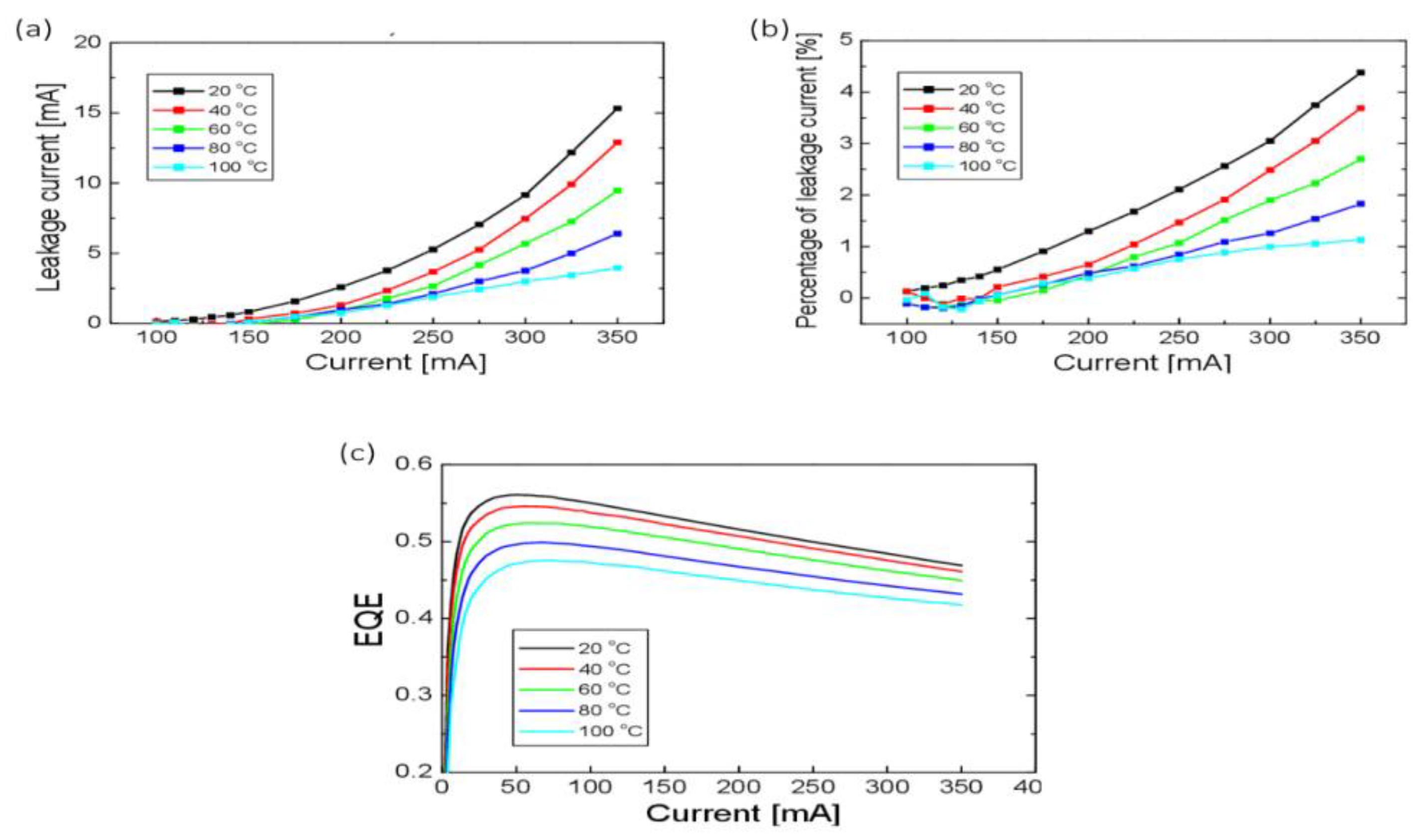
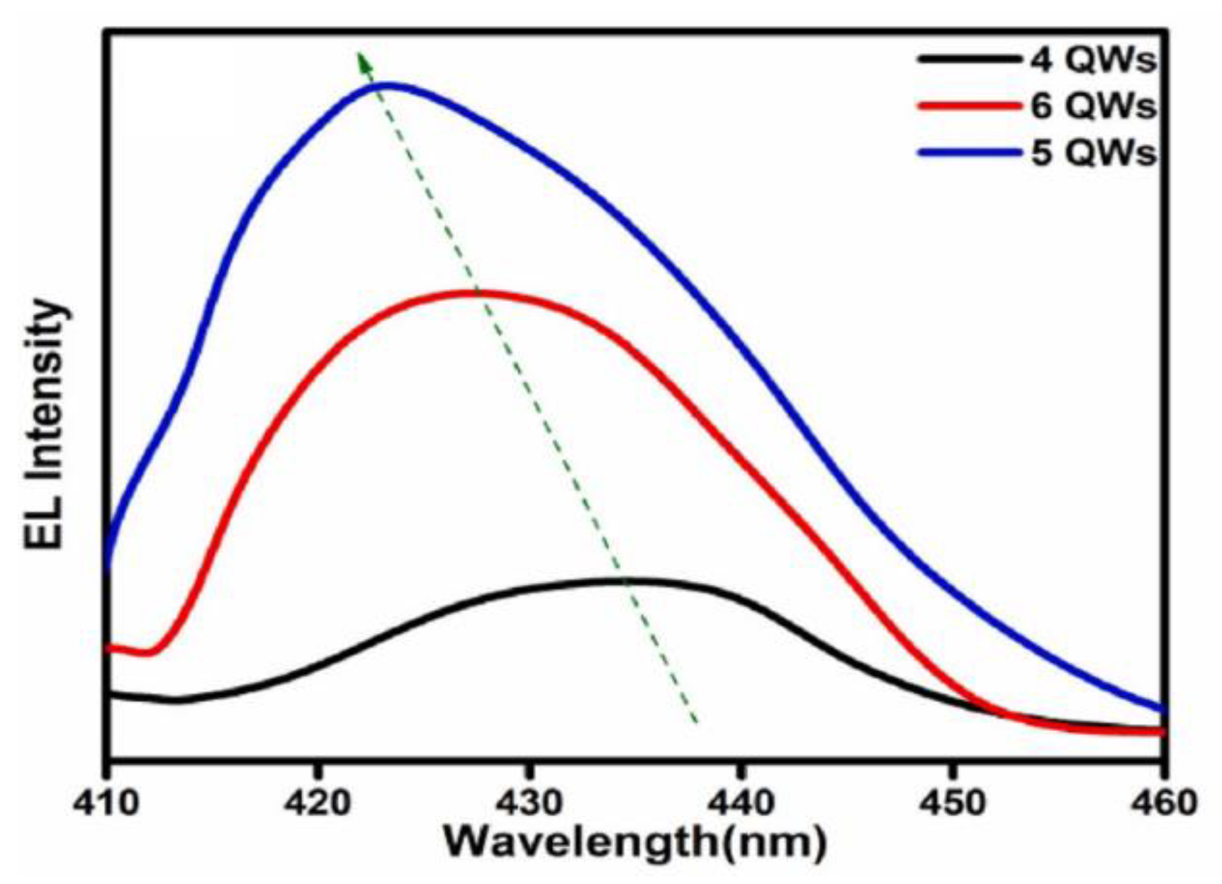