1. Introduction
III-nitride semiconductors, owing to their direct bandgap structure, have the capability to span a broad spectral range encompassing deep ultraviolet through near-infrared regions with alloy compositions [
1,
2]. The remarkable achievement of III-nitride semiconductors lies in the innovation and maturation of highly efficient InGaN-based blue and green light-emitting diodes (LEDs) [
3,
4], which have undergone commercial production for several years and have found extensive utilization in lighting and display applications [
5].
With the continuous advancement of research on LEDs by researchers, up until the present, InGaN-based micro-light-emitting diode (µLED) is considered to be the most promising next-generation display technology, which has greater advantages over liquid crystal display (LCD) and organic LED (OLED) in terms of brightness, resolution, contrast, power consumption, reliability, response speed, and thermal stability [
6]. As a result, it is now the ideal solution for numerous applications such as virtual reality (VR) and augmented reality (AR) [
7].
At present, most blue and green LEDs employ InGaN materials, while red LEDs utilize AlGaInP. Larger AlGaInP red LEDs are highly efficient, with a wall-plug efficiency (WPE) exceeding 50% under simulation, but their efficiency drops significantly when scaled down to the µLED range due to increased surface recombination and longer carrier diffusion lengths [
8]. AlGaInP red LEDs are also sensitive to temperature changes, which can cause efficiency losses due to carrier leakage [
9]. Integrating RGB μLEDs leads to mismatched light distribution between InGaN and AlGaInP, resulting in undesirable color shifts at different angles for micro-displays. Therefore, extending the emission wavelength of InGaN-based LEDs from blue/green to red offers a promising alternative to AlGaInP for micro-displays [
10].
However, the development of µLEDs still faces a substantial number of challenges. Among them, the high-quality fabrication and processes of InGaN-based red µLED are essential to achieve homogeneous and integrated full-color displays. In this regard, researchers continually make breakthroughs in various directions. Regarding transfer technologies, Chang et al. proposed the MDSAT method, which combines magnetic and dielectrophoresis (DEP) forces, for the rapid transfer of RGB LEDs onto large-area substrates, surpassing the previous FSA approach, and the transfer efficiency of RGB LEDs reached 99.99% by optimization [
11]. In the context of substrate optimization, White et al. presented their findings, demonstrating that red InGaN µLEDs achieved an EQE approaching 1% by employing semi-relaxed InGaN substrates on sapphire [
12]. Li et al., leveraging substrate optimization, have developed red µLEDs with an EQE of 4.5% by employing epitaxial tunnel junction (TJ) contact [
13]. In devices, Son et al. successfully enhanced the light output power and current density of GaN-based blue µLEDs by employing a µLED array structure. The enhancement rates of the output power were 174%, and in current density, it was enhanced by a factor of 2.1 when compared to that of the reference one [
14]. Mei et al. achieved heightened light extraction efficiency in GaN-based µLED devices by a suspended structure, which was 150% higher than that of the normal device [
15]. On the other hand, the size reduction tends to have a large impact on device performance. The rise in the body-to-surface area ratio of µLEDs as their size diminishes significantly affects their efficiency and leakage current. This phenomenon is attributed to the sidewall effect, which is induced by the plasma dry etching process, resulting in increased damage density and an elevated density of Shockley–Read–Hall (SRH) non-radiative recombination centers [
16]. Therefore, to improve the performance of small-sized red µLEDs, sidewall treatment is crucial in the device fabrication process.
There are currently two main types of treatments available to reduce the sidewall effect. One is the different types of aqueous solutions, which include KOH, tetramethylammonium hydroxide (TMAH), and H
3PO
4 [
17]. Yang et al. discovered that subjecting GaN-based LEDs to a 20% KOH treatment for 60 min at 100 °C can effectively optimize forward turn-on characteristics and suppress leakage currents [
18]. Wong et al. demonstrated that the combination of KOH chemical treatment and ALD sidewall passivation can effectively reduce the SRH non-radiative recombination and surface recombination caused by plasma damage by presenting the peak EQE (22–25% at 5–15 Acm
−2) of the blue InGaN LEDs (sizes range from 10–100 µm) [
19]. Sun et al. studied that tetramethylammonium hydroxide (TMAH) wet treatment optimized the micro trench at the bottom corner of the mesa sidewall [
20]. Mahitosh et al. improved the internal quantum efficiency of the near-band-edge emission peak from 3% to 7% through phosphoric acid [
21]. The other type of treatment is conducted by dielectric materials passivation, which includes but is not limited to SiO
2, SiNx, and Al
2O
3 [
17]. Hsu et al. used a hybrid SiO
2 micro/nanospheres antireflection coating to obtain a lower leakage current and achieve an 18.7% improvement in the light output power [
22]. Even for passivation layers of the same material, the use of different processes can have different effects on the performance of the LEDs. Lee et al. conducted an investigation demonstrating that the ALD-Al
2O
3/PECVD-SiO
2 passivation layer exhibits superior performance in suppressing sidewall effects compared to the PECVD-SiO
2 layer alone. Furthermore, at lower current densities, the double passivation layer achieves peak external quantum efficiency, surpassing that of the single-layer counterparts [
23]. Chevtchenko et al. proved that a reduction of the leakage current can be observed after SiNx passivation, and passivation eliminates surface states and surface recombination [
24]. Kim et al. applied AlN/Al
2O
3 deposition on p-GaN to acquire LEDs with higher light-emission efficiency and a minimized leakage current [
25].
In this research, red InGaN-based µLED arrays with different sizes (5 µm × 5 µm, 10 µm × 10 µm, 15 µm × 15 µm, 20 µm × 20 µm) were successfully fabricated, based on which we systematically investigated the effects of treatment with or without KOH on the sidewalls. Characterization of the sidewall morphology and electrical and optical properties of the device were conducted through scanning electron microscopy (SEM), current–voltage curves, and electroluminescence (EL), aiming to assess its performance.
2. Materials and Methods
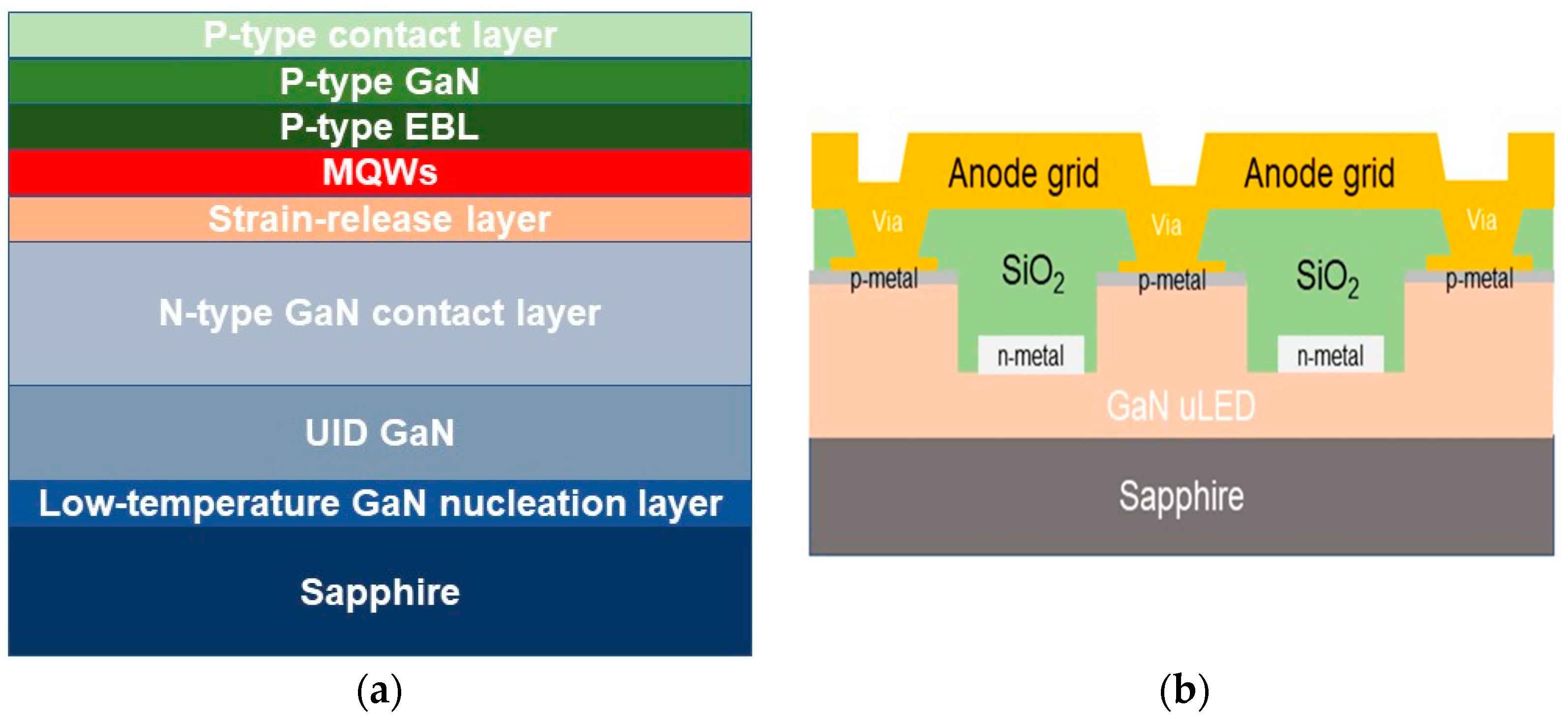
The red LED arrays were fabricated on GaN epi layers, which were grown on a 4-inch sapphire substrate by the metal-organic chemical vapor deposition (MOCVD) method by Suzhou Hanhua Semiconductors Ltd., (Suzhou, China). The epitaxial structure is shown in
Figure 1a. The LEDs were grown on 4-inch planar sapphire substrates. The epitaxial growth started with 30 nm low-temperature GaN, which serves as a nucleation layer for subsequent growth. Then, a 1.5 µm-thick un-intentionally doped (UID) GaN layer was grown until its surface coalesced, which was followed by a 2.5 µm n-type GaN contact layer doped with Si to 5 × 10
18 cm
−3. After the n-type contact layer, a 200 nm InGaN-based strain-release layer and active region (multiple-quantum wells, MQWs) were deposited. On top of the active region, a p-type electron-blocking layer (EBL) as well as a p-type GaN and a p-type contact layer were grown. All the p-type layers were doped with Mg.
After the epitaxial growth, the LED materials were p-type activated by thermal annealing in a furnace. The materials were then characterized by photoluminescence (PL) with a laser wavelength at 405 nm, as well as electroluminescence (EL) with an indium dot directly on the wafer surface. The diameter of the indium dot was around 1.5–2.0 mm. The LED wafers were then fabricated into devices. The device structure ensures that the light is reflected towards the substrate direction during the optical measurement, and the detailed fabrication processes are described below, and the schematic of the device process is depicted in
Figure 2.
Initially, to remove the contaminations on the surface of the wafers, organic and acid cleaning is performed. Then, a 20 nm thick NiAu layer is deposited on the p-GaN using electron beam evaporation, followed by an annealing process in an oxygen atmosphere at 550 °C for 1 min to facilitate the formation of improved ohmic contacts. For mesa formation, photolithography is employed in conjunction with an 800 nm thick silicon dioxide (SiO
2) hard mask. The SiO
2 hard mask is grown by plasma-enhanced chemical vapor deposition (PECVD), followed by patterning and etching of SiO
2 using a fluorine-based inductively coupled plasma (ICP) etching technique. LED mesa is formed by a chlorine-based inductively coupled plasma reactive ion etching process reaching the n-GaN layer. Then, sidewall treatment is conducted on selected wafers by soaking them in a KOH solution at 80 °C for 3 min. The SiO
2 hard mask serves to preserve the integrity of the top surface of the device’s p-GaN, including the NiAu layer. After that, the n-contacts grid pattern is deposited on the n-GaN surface between LEDs. Subsequently, a 2.5 µm thick SiO
2 passivation layer is deposited, and the wafer surface is planarized by a chemical mechanical polishing (CMP) process, concurrently reducing the thickness of the SiO
2 to 200 nm, followed by a process to open the p-metal of each LED. Following this, an etching process is employed to remove the SiO
2 layer on the n-pad, ensuring that the n-pad is exposed for subsequent electrical and optical measurement purposes. In each array that contains tens of thousands of LEDs, we placed an anode grid consisting of TiAl, which is deposited by sputtering, to shoot the
p-contact of all pixels to facilitate the electrical and optical measurement by driving them together. The sizes of the LEDs in the different arrays include 5 × 5 µm, 10 × 10 µm, 15 × 15 µm, and 20 × 20 µm. The cross-section structure of the array is illustrated in
Figure 1b.
3. Results
In the PL (photoluminescence) measurement conducted at room temperature with a laser wavelength of 405 nm, we obtained photoluminescence images of the entire epi wafer surface. As is shown in
Figure 3, these images reveal the distribution of Wp (peak wavelength) and FWHM (full width at half maximum) in different regions, thereby providing spatial distribution information about the material properties within the epi wafer. In the figure, it is observed that the Wp of both epi wafers is centered at 673 nm. Furthermore, the FWHM of the epi wafer intended for the KOH wet treatment is concentrated at 87 nm, while the FWHM for the other wafer is centered at 90 nm. These two epi wafers exhibit similar characteristics. By analyzing the PL mapping figure, we can observe that these two epi wafers exhibit good uniformity in terms of Wp and FWHM, which meets our requirements for utilizing them in subsequent processes.
Figure 4 presents the EL (electroluminescence) spectral data of the epi wafers obtained at an injection current of 109 mA. The blue line represents the epi wafer intended for subsequent KOH sidewall treatment, while the red line represents the epi wafer that will not undergo KOH wet treatment. In the figure, we observe that the properties of these two epi wafers are similar, with comparable values for Wp and FWHM, showing minimal differences. This phenomenon is attributed to the identical epitaxial conditions employed for both epi wafers. Specifically, the epitaxial structure, composition of each layer, layer thickness, doping conditions, and other relevant parameters were maintained uniformly across both epi wafers. Therefore, these two epi wafers can be further processed, effectively controlling variables for subsequent comparisons of various properties.
Figure 5a,b show scanning electron microscope (SEM) images for a comparison between the LED mesa with KOH wet treatment and the one without. In this context, we have selected a mesa with a size of 20 µm for our illustrative example. From the figure, it is obvious that after the dry etching process, the GaN sidewalls exhibit a significantly roughened texture. In contrast, after wet KOH etching, the GaN sidewalls appear considerably smoother, indicating an effective removal of sidewall GaN material. This treatment serves to reduce the density of the leakage path on the sidewalls.
Figure 6 shows the current–voltage (I–V) curves of array devices of different sizes with or without KOH wet etching.
Figure 6a displays the I–V curves for an array device comprising 10,000 pixels. In this array, the individual LED size is 20 µm. The blue line represents the group in which KOH sidewall etching was performed, while the red line corresponds to the control group, which did not undergo KOH etching. In terms of leakage current, we find that at −5V, the leakage current density without KOH is 0.2965 A/cm
2 and the leakage current density with KOH wet treatment is 0.0131 A/cm
2, which is obviously lower. Similar trends are observed on all arrays in different sizes: 0.007 A/cm
2, 0.0012 A/cm
2, and 0.0057 A/cm
2 for 15 µm, 10 µm, and 5 µm size pixels with KOH treatment and 0.0144 A/cm
2, 0.0057 A/cm
2, and 0.6652 A/cm
2 for the same size pixels without treatment. Through a comparative analysis of data, it is observed that the leakage current has decreased by a minimum factor of 2.06 and by a maximum of two orders of magnitude. Both scenarios exhibit a noticeable inhibitory effect on the leakage current, which indicates that KOH sidewall wet etching can eliminate the defects caused during dry etching well, allowing the leakage current to be reduced to an ideal state.
In the presented data, the effectiveness of KOH wet etching in mitigating the leakage current is consistent through a wide range of device sizes. Furthermore, there exists a substantial correlation between the density of leakage current and device size. Specifically, for smaller-sized LEDs, as their dimensions decrease, the body-to-surface area ratio steadily increases. Consequently, this heightened ratio leads to an augmentation in surface states within the LED structure. Surface states, in this context, refer to electronic states positioned within or near the energy bandgap or band edges, which are capable of capturing and releasing charge carriers, such as electrons. In the case of smaller-sized LEDs, the relatively larger surface area compared to volume facilitates a more pronounced influence of these surface states on electron dynamics. This influence results in an increase in leakage current density. Remarkably, at a dimension of 5 µm, the LED array exhibits the highest leakage current density. However, KOH wet treatment to the sidewalls significantly ameliorates this issue, elevating the leakage current density to a level commensurate with arrays of other sizes. This improvement arises primarily from the ability of KOH wet etching to optimize the removal of damage, defects, and impurities introduced during dry etching processes. This optimization reduces lattice imperfections, refines electric field distribution, diminishes electron scattering in proximity to sidewalls, and minimizes leakage pathways. KOH wet etching serves to lower surface state density, further reducing the impact of surface states on electron behavior, thus contributing to the reduction of the leakage current.
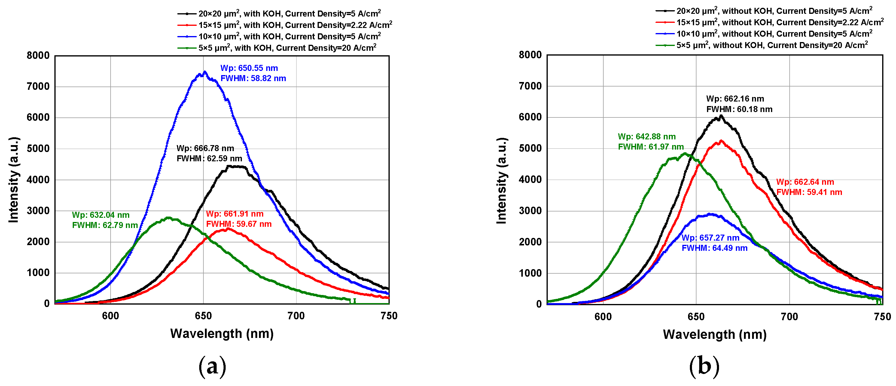
Figure 7 shows the EL spectra obtained at the injection current of 200 mA for different-sized arrays, where Wp and FWHM can be obtained for cases with (
Figure 7a) and without (
Figure 7b) KOH treatment. From the figures, we see that the Wp consistently exceeds 632 nm, with FWHM ranging around 60 nm. Comparing the epi wafer data in
Figure 4, we observe that after device processing, Wp and FWHM have not undergone significant changes. This indicates that our device processing has not adversely affected the material’s inherent performance. Notably, neither Wp nor FWHM exhibits any significant trends resulting from KOH wet treatment. Furthermore, both pictures show that at the same injection current, a reduction in size corresponds to a decrease in Wp. The underlying cause of this phenomenon is the blue shift at a higher injection current density.
To further investigate the blue shift effect, we also tested the relationship between Wp and the current for four different sizes, as shown in
Figure 8, where the blue and red curve represents treatment with and without KOH, respectively. From these data, it can be seen that under an increased current, arrays of varying sizes and processing methods all exhibit a blue shift phenomenon. The change of Wp from an injection current of 100 mA to 300 mA (approximately from 1.11 A/cm
2 to 30 A/cm
2) is usually within 3–8 nm, regardless of the size of the pixel. Furthermore, there appears to be no significant correlation between the blue shift in Wp and the application of KOH wet etching. We believe it is mostly dependent on the red LED epitaxy structures and growth process rather than on the device fabrication process. Usually, the blue shift in InGaN-based LEDs is the result of the screening in the quantum-confined Stark effect (QCSE) and band-filling effects [
26], which is especially obvious in high In-concentration for long wavelength MQW structures. The LED wafer we used for this study contains complicated stress relief structures beneath the active region. Compared with other commercially available red GaN epi, our structure shows much elevated performance in terms of blue shift reduction.
Figure 9 provides a comparison of thelight output power (LOP) of µLEDs between arrays with different sizes. In each figure, the blue curve represents the trends in LOP for arrays subjected to KOH wet treatment, while the red curve signifies the trends for arrays without KOH. The figures clearly indicate that as the injection current density increases, the LOP of LEDs with different sizes and processing methods exhibits a consistent and monotonic increase. Furthermore, it is evident from the figures that arrays with KOH display higher LOP compared to those without KOH treatment. We propose that this occurrence is due to the reduced leakage current in arrays with KOH and allows a more efficient conversion from electrical power into optical power. This suggests that the KOH wet treatment, by modifying the sidewalls and reducing non-radiative recombination centers, can effectively enhance the optical performance of µLEDs.
In order to verify the EL (electroluminescent) efficiency of the device, we measured the efficiency droop for a 10 µm size µLED array, and the result is shown in
Figure 10. It is important to note that the efficiency is presented as a relative value rather than an absolute one, so it is only meaningful in comparing the efficiency between devices in the same geometry. The blue curves represent trends observed in arrays with KOH wet treatment, while the red curves represent trends in arrays without KOH. This figure obviously demonstrates that, as the current density steadily increases, electroluminescent efficiency gradually decreases. We attribute this phenomenon to the increased rate of non-radiative recombination as the injected carrier density goes higher. This is well-known as the efficiency droop effects observed in all InGaN-based LEDs. It is noteworthy that, following KOH wet treatment, although the LED efficiency surpasses that of the ones without KOH treatment, it also drops faster as the current goes higher. This observation suggests that the cause for the droop is less likely to originate from the surface defect but is more related to material defects in the epi structure.
4. Conclusions
In our study, we have successfully fabricated red µLED arrays with sizes ranging from 5 µm to 20 µm and demonstrated that their optoelectronic performance can be enhanced by KOH wet treatment on pixel sidewalls. The KOH wet treatment manifests obvious morphology changes on sidewalls and significant reductions in leakage current. Sidewall etching with KOH is an irreversible process, where the severed leakage pathways cannot be recovered, effectively impeding the generation of leakage current. The extent of improvement is more pronounced for smaller-sized µLEDs, particularly those with a size of 5 µm.
Regarding optical performance, Wp and FWHM remained largely unaffected by different device sizes and treatments. Meanwhile, LOP exhibited a monotonic increase with a rising current density. The minimum Wp blue shift observed on the different-size arrays indicates superb epi-quality from the MOCVD growth of epi structure. However, in terms of electroluminescent efficiency, although the efficiency for the treated array is better than the non-treated counterpart, it also drops faster. This suggests that the KOH wet treatment to the µLED pixel sidewalls has great potential to be applied in the device fabrication process to suppress surface non-radiative recombination and improve the optical performance. The efficiency droop is more likely to be related to epi defects, which need extra optimization. In this study, the successful fabrication of small-sized red µLEDs and the optimization by KOH wet treatment of the processes provide support and impetus for expanding their application areas and enhancing display and lighting qualities.


