Article

Performance Investigation of a Proposed Flipped npn Microstructure Silicon Solar Cell Using TCAD Simulation

by
Marwa S. Salem
1,2,
Abdelhalim Zekry
3,
Ahmed Shaker
4,*,
Mohamed Abouelatta
3,
Mohamed M. ElBanna
4,
Tariq S. Almurayziq
5,
Rabie A. Ramadan
1,6 and
Mohammad T. Alshammari
5
1
Department of Computer Engineering, College of Computer Science and Engineering, University of Ha’il, Ha’il 55211, Saudi Arabia
2
Department of Electrical Communication and Electronics Systems Engineering, Faculty of Engineering, Modern Science and Arts University (MSA), Cairo 12566, Egypt
3
Department of Electronics and Communications, Faculty of Engineering, Ain Shams University, Cairo 11566, Egypt
4
Department of Engineering Physics and Mathematics, Faculty of Engineering, Ain Shams University, Cairo 11566, Egypt
5
Department of Computer Science and Information, Computer Science and Engineering College, University of Ha’il, Ha’il 55211, Saudi Arabia
6
Computer Engineering Department, Faculty of Engineering, Cairo University, Giza 12613, Egypt
*
Author to whom correspondence should be addressed.
Crystals 2022, 12(7), 959; https://doi.org/10.3390/cryst12070959
Submission received: 20 June 2022 / Revised: 4 July 2022 / Accepted: 6 July 2022 / Published: 9 July 2022
(This article belongs to the Special Issue Silicon and Graphene Based Materials and Related Devices)

Abstract

:
This work aims at inspecting the device operation and performance of a novel flipped npn microstructure solar cell based on low-cost heavily doped silicon wafers. The flipped structure was designed to eliminate the shadowing effect as applied in the conventional silicon-based interdigitated back-contact cell (IBC). Due to the disappearance of the shadowing impact, the optical performance and short-circuit current density of the structure have been improved. Accordingly, the cell power conversion efficiency (PCE) has been improved in comparison to the conventional npn solar cell microstructure. A detailed analysis of the flipped npn structure was carried out in which we performed TCAD simulations for the electrical and optical performance of the flipped cell. Additionally, a comparison between the presented flipped microstructure and the conventional npn solar cell was accomplished. The PCE of the conventional npn structure was found to be 14.5%, while it was about 15% for the flipped structure when using the same cell physical parameters. Furthermore, the surface recombination velocity and base bulk lifetime, which are the most important recombination parameters, were studied to investigate their influence on the flipped microstructure performance. An efficiency of up to 16% could be reached when some design parameters were properly fine-tuned. Moreover, the impact of the different physical models on the performance of the proposed cell was studied, and it was revealed that band gap narrowing effect was the most significant factor limiting the open-circuit voltage. All the simulations accomplished in this analysis were carried out using the SILVACO TCAD process and device simulators.

1. Introduction

Recently, a lot of studies have concentrated on the cost reduction of photovoltaic (PV) modules used in PV systems. The primary cause for the elevated cost of silicon PV solar cells (SCs) is caused by the manufacturing of relatively low-doped high-quality Si wafers [1]. Additionally, to be able to use the commercial silicon solar cells, the thickness has to be in the range of hundreds of micrometers and even higher (submillimeter) to extend the light absorption [2]. Numerous research works deal with reducing the PV cells’ high cost. Several examples include thin-film SCs, which are manufactured from Copper Indium Gallium Sulfide and Cadmium Telluride (CdTe) [3]. The main objective of using these technologies is to attain efficiencies comparable to crystalline Si (c–Si)-based PV solar cells, while adopting fragile absorber layers. Nevertheless, such technologies produce added problems, such as toxicity and scarcity, which are considered environmentally harmful. In addition, deposition systems are required which expand their fabrication cost. From another point of view, thin-film Si cells, which are produced from amorphous silicon, have stability concerns [4].
There is another alternative which is used to lower the cost of c–Si PV cells. It is based on the reduction in the Si wafer’s thickness from its traditional value of 180 to 80 μm. Such thickness is practically deemed a lower limit [5]. Unfortunately, the decrease in the thickness of silicon wafers usually requires light management techniques to achieve the maximum absorption of the input solar radiation spectrum despite the lowered thickness.
A promising solution to the challenge of achieving a low cost while maintaining reasonable efficiencies is to exploit Si nano- or microstructures [6,7,8,9]. The advantages of utilizing such structures include enhanced light-trapping capabilities and invoking shorter diffusion lengths, which result in high carrier collection efficiency [10]. This can be accomplished by realizing a high aspect ratio and high-doped p-n junctions in the radial direction [11]. Based on this concept, decoupling of the absorbed photons’ path and minority carrier diffusion direction are achievable [12]. B. Dou et al. have reported an efficiency of 11.94% for a radial p-n junction solar cell [13]. The mentioned cell was fabricated based on a Si nanopillar array that was synthesized from p-type Si substrates. In addition, Si micro-gratings with vertical sidewall electrodes have been fabricated, resulting a solar cell having a short-circuit current and an efficiency of 19.54 mA/cm2 and 7.8%, respectively [14]. Moreover, a high-performance micropillar silicon structure with a Cu nanoparticle solar cell was synthesized, and a cell efficiency of 11.5% was attained [15].
Using inexpensive materials, such as highly doped Si wafers, to achieve low-cost solar cells is one of the most attractive alternatives. Such cheap wafers, however, have a significant disadvantage as they have a high level of defects, implying low minority carrier diffusion lengths [16,17]. Thus, the charge carrier collection diminishes, and the solar cell performance degrades. To overcome such a problem, the light-generated carriers in such inexpensive wafers need to be vertically generated and laterally collected [18]. Such an idea opens a route for employing low-quality highly doped Si wafers, which are characterized by their low cost and commercial availability for solar cell fabrication [19,20]. Recently, a proposed npn microstructure SC, which was based on a heavily doped Si wafer as a base material, demonstrated an initial efficiency of 10.7% [21]. After the optimization of its technological parameters, it provided about 14.5% efficiency [22].
In this work, the performance of flipping the proposed optimized npn microstructure SC was investigated. The key purpose of flipping the structure was to eliminate the shadowing effect. First, a qualitative analysis explaining the reason for using the flipped npn structure is presented. In this analysis, a proposed configuration of the flipped npn microstructure is examined in comparison to the npn solar cell microstructure. The arrangement and advantages of the flipped npn structure are qualitatively discussed. Second, the qualitative analysis was verified quantitatively by making use of TCAD process and device simulators. A thorough electrical and optical description for the flipped structure in comparison with the npn microstructure was carried out. In addition, the influence of the recombination velocity and base lifetime on the performance of the flipped and conventional npn microstructures was investigated.
The paper is coordinated as follows. Section 2 presents the key design parameters of the proposed flipped npn microstructure. Section 3 describes the physical models used in the device simulation. Section 3 illustrates the simulation steps of the proposed flipped npn microstructure by using SILVACO TCAD. Further, Section 3.1 discusses the impact of the n+ sidewall emitter surface treatments on the performance of the structure. Moreover, the influence of the P+ base lifetime is investigated in Section 3.2. Finally, Section 4 draws the conclusions of our work.

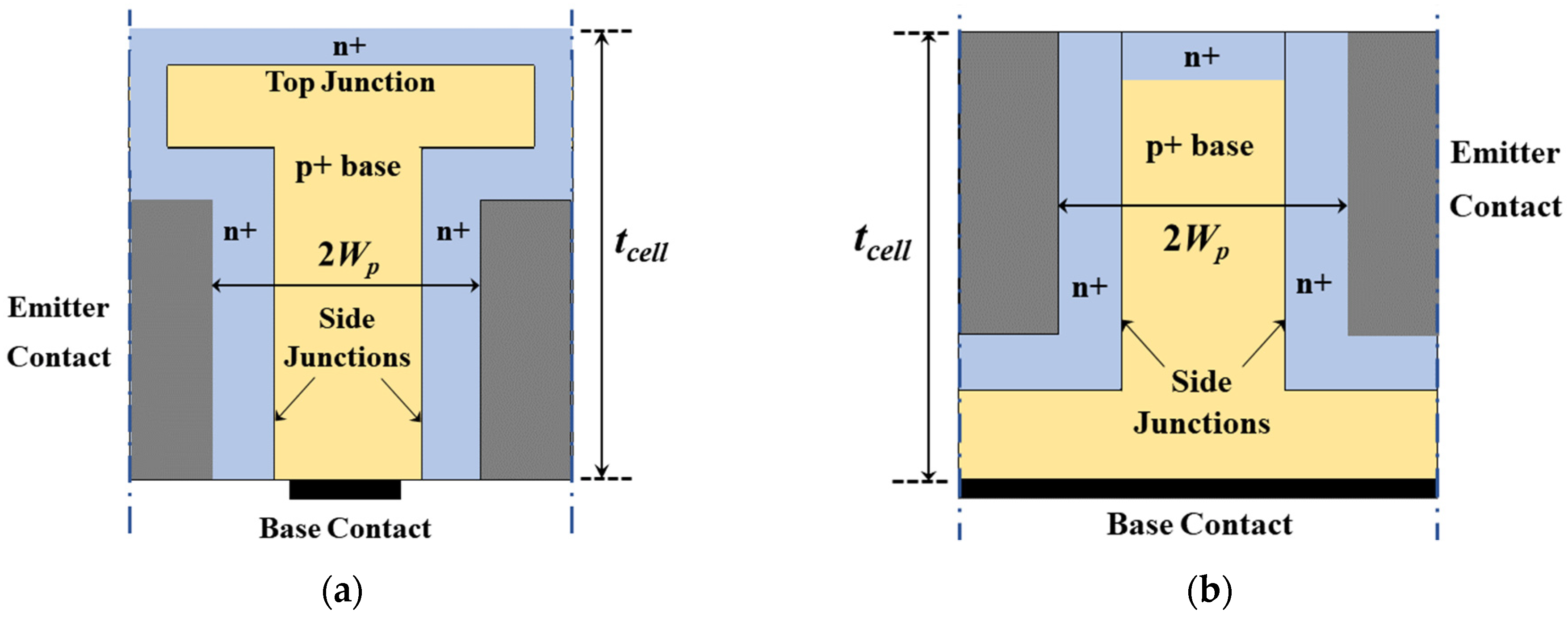
2. Key Design Parameters of the Proposed Flipped npn Microstructure

In this section, a detailed analysis for the flipped npn solar cell microstructure is carried out. Firstly, a qualitative analysis explaining the objective of using the flipped npn structure is presented. Figure 1 shows the proposed flipped npn structure in comparison with the conventional npn microstructure [22]. The main objective of flipping the npn solar cell microstructure (Figure 1a) was to eliminate the effect of shadowing on the structure performance as seen in the conventional structure (Figure 1b), in which the emitter contact produces shadowing. Therefore, the flipped structure provides a larger area exposed to the incident solar radiation than the conventional cell. Consequently, it was qualitatively expected that the optical performance of the flipped structure would be better than that of the conventional npn microstructure.
In this study, the proposed flipped npn solar cell microstructure has the same design parameters as the conventional npn structure discussed in our previous work [22], except that the flipped structure has a buried emitter which minimizes the shadowing effect, as is depicted in Figure 1a. The emitter perimeter of the flipped solar cell is larger than that of the conventional solar cell. The p + volume, which is considered as the active region, is also larger in the flipped solar cell. The main parameters of the flipped structure are summarized as follows. The p+ base width is 2Wp where Wp is the width of the base region, which is chosen to be Wp = 8 µm, while the width of the n+ side wall emitter is denoted by Wn and is set to 0.18 µm, and the thickness of the cell is termed by tcell and is taken to be 80 µm, a typical value for thin wafers. The doping levels of the p+− base, n+-side wall and top regions are Np+,base, Nn+,emitter and Nn+,top, respectively, where their values are Np+,base = 1018 cm−3 and Nn+,emitter = Nn+,top = 5 × 1019 cm−3. The n+ layer thickness is tn+, which is fixed at 0.1 µm by adjusting the diffusion process through the process simulator. The criteria for choosing such design parameters values were thoroughly argued in our previous work [19,22,23].

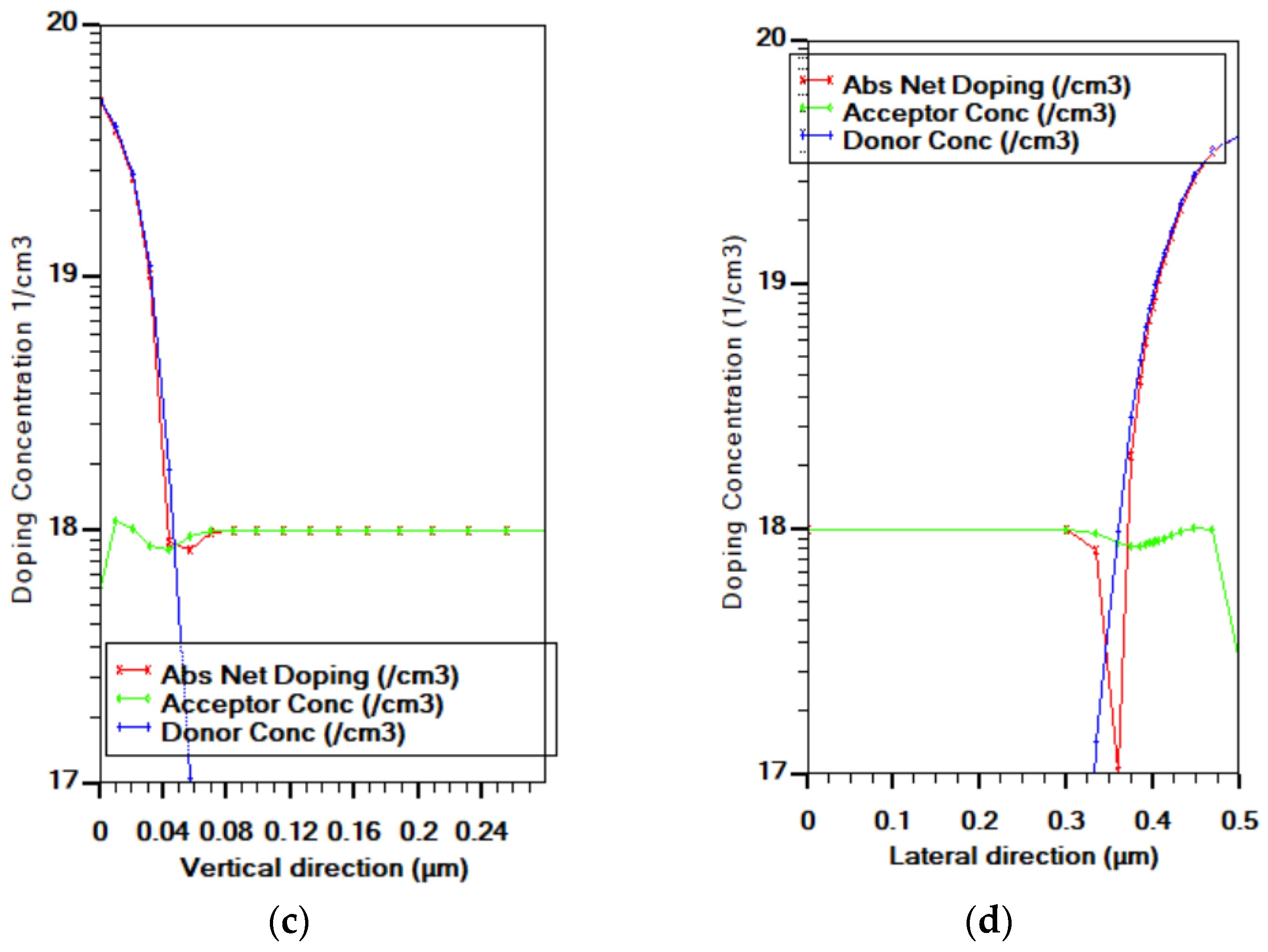
3. Simulation of the Proposed Flipped npn Microstructure Using SILVACO TCAD

The simulation of the proposed flipped npn microstructure was executed by exploiting the SILVACO process and device simulators through the subsequent steps. First, the flipped npn microstructure SC was realized by using the SILVACO process simulator (Athena) [24]. Next, the structure was simulated by applying the SILVACO device simulator (Atlas) [25]. At this stage, the major physical models necessary for simulation were incorporated. These include concentration-dependent mobility (conmob), field-dependent mobility (fldmob), concentration-dependent Shockley–Read–Hall recombination (consrh), Auger recombination (auger) and band gap narrowing (bgn) models. The minority carrier lifetime of the emitter was extracted from the literature [26,27,28,29]. Figure 2 demonstrates the flipped structure, which was created using the SILVACO Athena process simulator [24].
Here, a comparison between the conventional npn and the flipped npn structure optical and electrical performance was performed with the device simulator. The optical performance was examined in terms of the external quantum efficiency, while the electrical performance was inspected by the illuminated J–V characteristics under AM1.5G solar spectrum. From the J–V characteristic, all their electrical photovoltaic parameters, Jsc, Voc, FF and PCE, were compared. Figure 3 shows the quantum efficiency (Figure 3a) and illuminated J–V characteristics (Figure 3b) for the npn and the flipped npn microstructure. As is depicted in Figure 3a, the quantum efficiency of the flipped structure is greater than that of the conventional cell, resulting in a higher short-circuit current as evident from Figure 3b. This is because the flipped structure has no shadowing compared to the conventional npn microstructure. Moreover, Table 1 summarizes the extracted electrical performance photovoltaic parameters, Jsc, Voc, FF and PCE, for the two structures. It can be deduced from the table that the flipped structure has higher conversion efficiency. The efficiency of the proposed flipped structure is 0.5% above the conventional cell, which is considered a good enhancement.
The improvement in the PCE did not result in a very high difference from the conventional cell because of the mutual operation of two junctions. The main junction is the lateral junction, while the top junction is considered a secondary junction. When flipping the conventional npn structure, the top junction performance improved; however, this improvement does not significantly reflect a high PCE because of the minor contribution to light absorption of the top junction compared to the principal sidewall junction.
To provide a physical explanation for the reduction in the Voc of the flipped structure compared to that of the conventional cell, the dark J–V characteristics were simulated, as represented in Figure 4. The equivalent circuit of the two-diode model could effectively signify the dark behavior of the presented cells. The main dark parameters, reverse saturation current Jo, ideality factor n and series resistance Rs, for both diodes were consequently extracted and are listed in Table 2. The Voc can be expressed analytically by the following approximate equation:
V o c , a n a n V T ln ( J s c J o )
where VT is the thermal voltage. Based on this expression, we calculated the Voc,ana for the flipped and conventional cells where the values of the second diode parameters are used, as provided in Table 2, as this is the effective diode around the Voc. The analytical values were near those found from simulation, also implying the same trend of the open-circuit voltage, so the analytical solution was confirmed by the TCAD results.

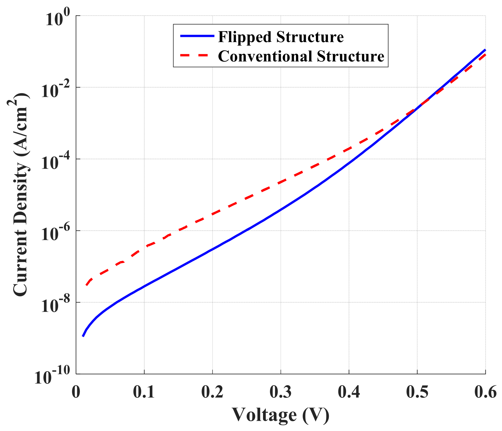
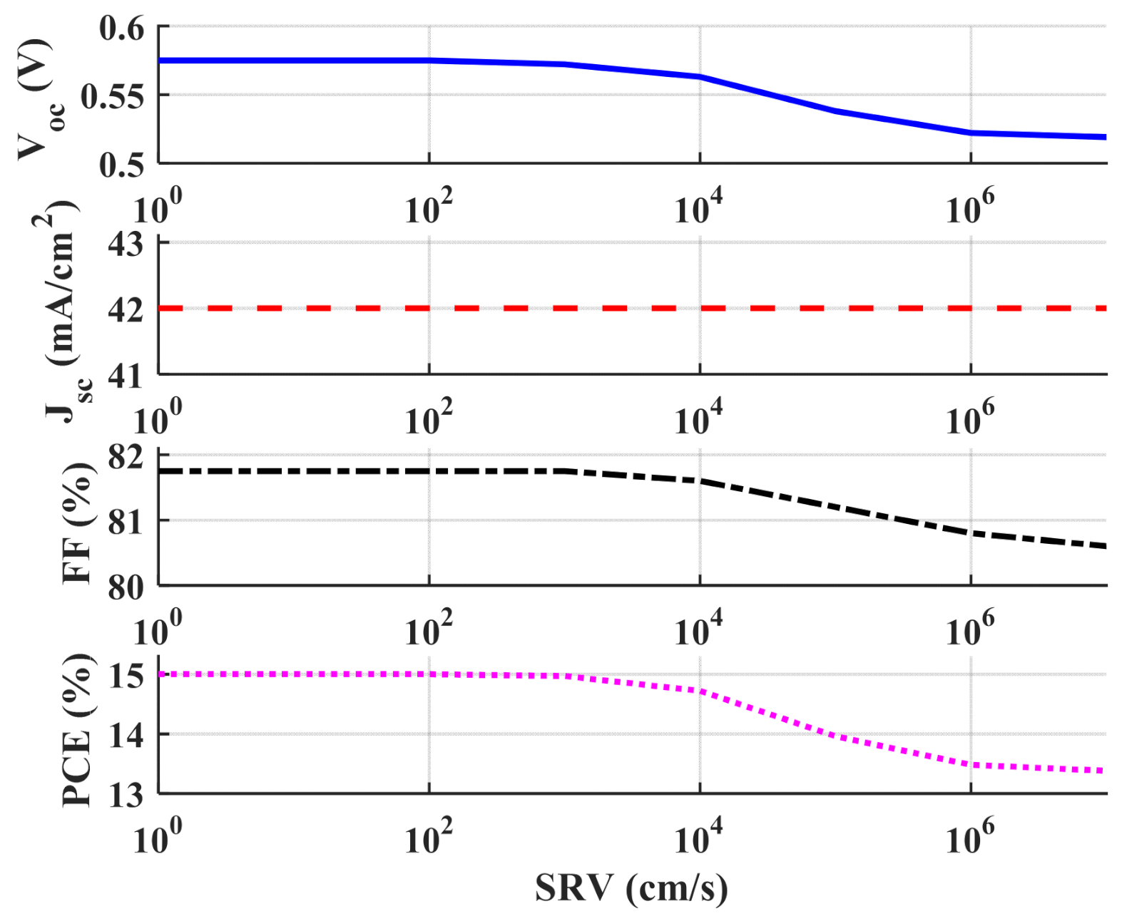
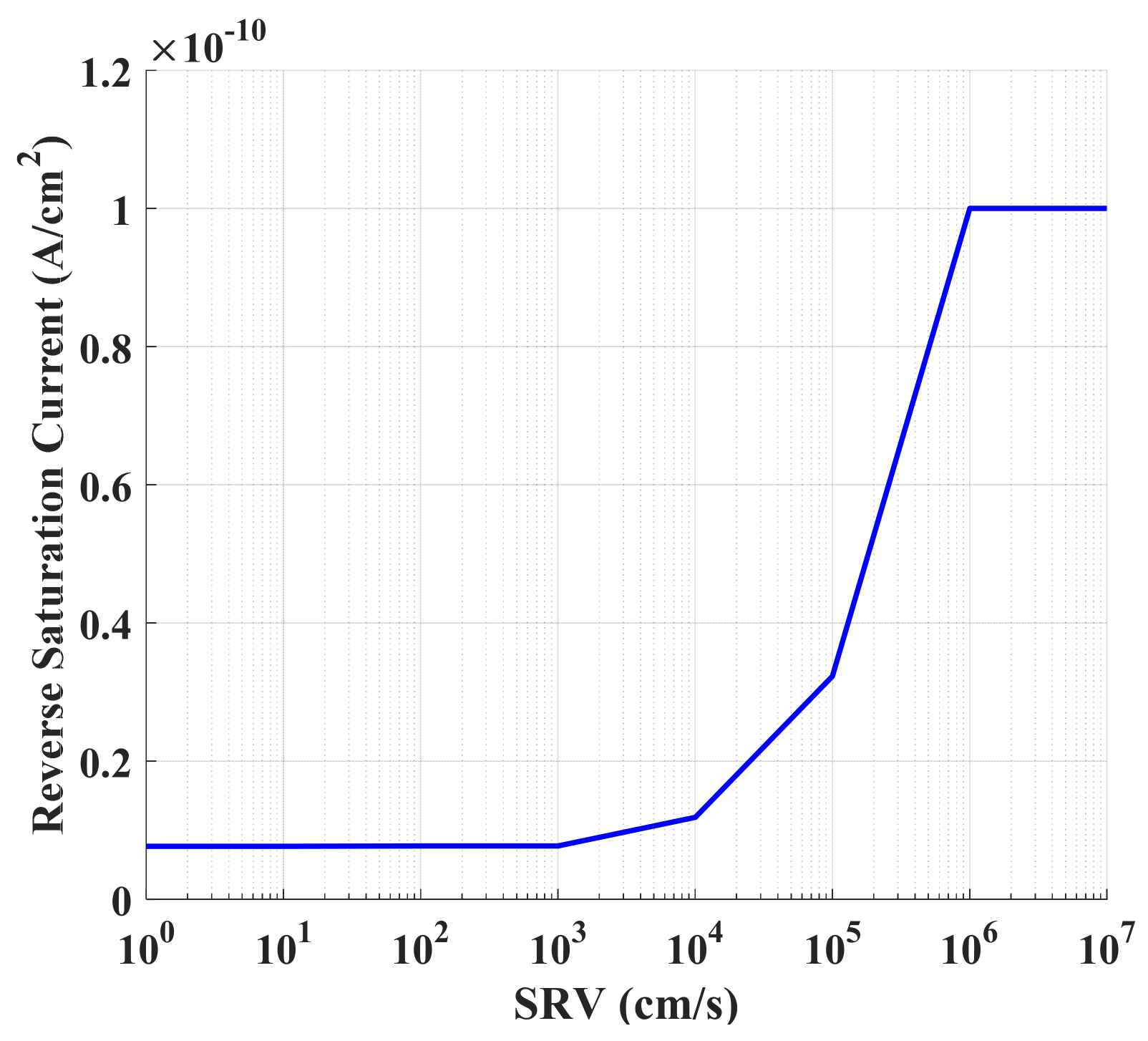
3.1. Effect of Different n+ Sidewall Emitter Surface Treatments

Surface recombination velocity (SRV) is a crucial parameter which significantly influences the solar cell operation. A high value of SRV produces the creation of a dead layer [30]. The photo-generated carrier rates are reduced due to increased SRV. SRV impacts both the dark and illumination performance of the solar cell [31,32,33,34,35]. Throughout this subsection, the impact of various n+ emitter surface treatments on both optical and electrical performance parameters of the conventional and flipped structures is illustrated. There are four different types of surfaces in solar cells. The first type is the ideal non-recombining contact (with SRV = 1 cm/s), the second is the recombining contact with low surface recombination velocity using good and clean oxide, such as the gate oxide in MOS transistors, the third type is recombining contact with relatively high SRV (in the order of 104 cm/s and higher) using non-clean oxide, such as FOX oxide in a MOS transistor, and the fourth type is ohmic contact, having the highest SRV, up to 107 cm/s (which is corresponding to the saturation velocity carriers) [36,37,38,39,40]. So, the analysis was performed for different values of surface recombination velocity, ranging from 1 to 107 cm/s.
Figure 5 shows the Voc, Jsc, FF and PCE of the different values of SRV of the flipped structure. It is obvious that from 1 to 104 cm/s, representing the ideal contact and good oxide, the structure performance parameters are not affected. The cell performance start to degrade starting from 104 cm/s. The most interesting result is that the illumination characteristics are not affected by SRV variation as the study of SRV is concerned with the sidewall emitter. The influence is deeply apparent in the degradation of Voc. This result is expected as by increasing SRV, the reverse saturation current increases; thus, Voc decreases. Concerning the fill factor, it is reversely affected by the reverse saturation current; thus, the fill factor decreases. As for the conversion efficiency, as it is a function of Voc and FF, it decreases. The above discussion suggests aluminum (Al) should not be directly deposited on the n+ sidewall emitter without firstly passivating it. Additionally, the passivation must occur with a relatively low SRV, up to 104 cm/cm, to not degrade the structure performance.
Again, to explain the influence of SRV on the Voc, we simulated the dark characteristics for different cases of SRV. The extracted reverse saturation current of the equivalent diode around the Voc is displayed in Figure 6. The reverse saturation current is constant for a SRV up to 103 cm/s. Then, it slightly increases up to 104 cm/s followed by a significant increase up to SRV = 106 cm/s. Beyond this value, the reverse saturation current becomes almost constant. The trend of the reverse saturation current is the same as for Voc, as expected.

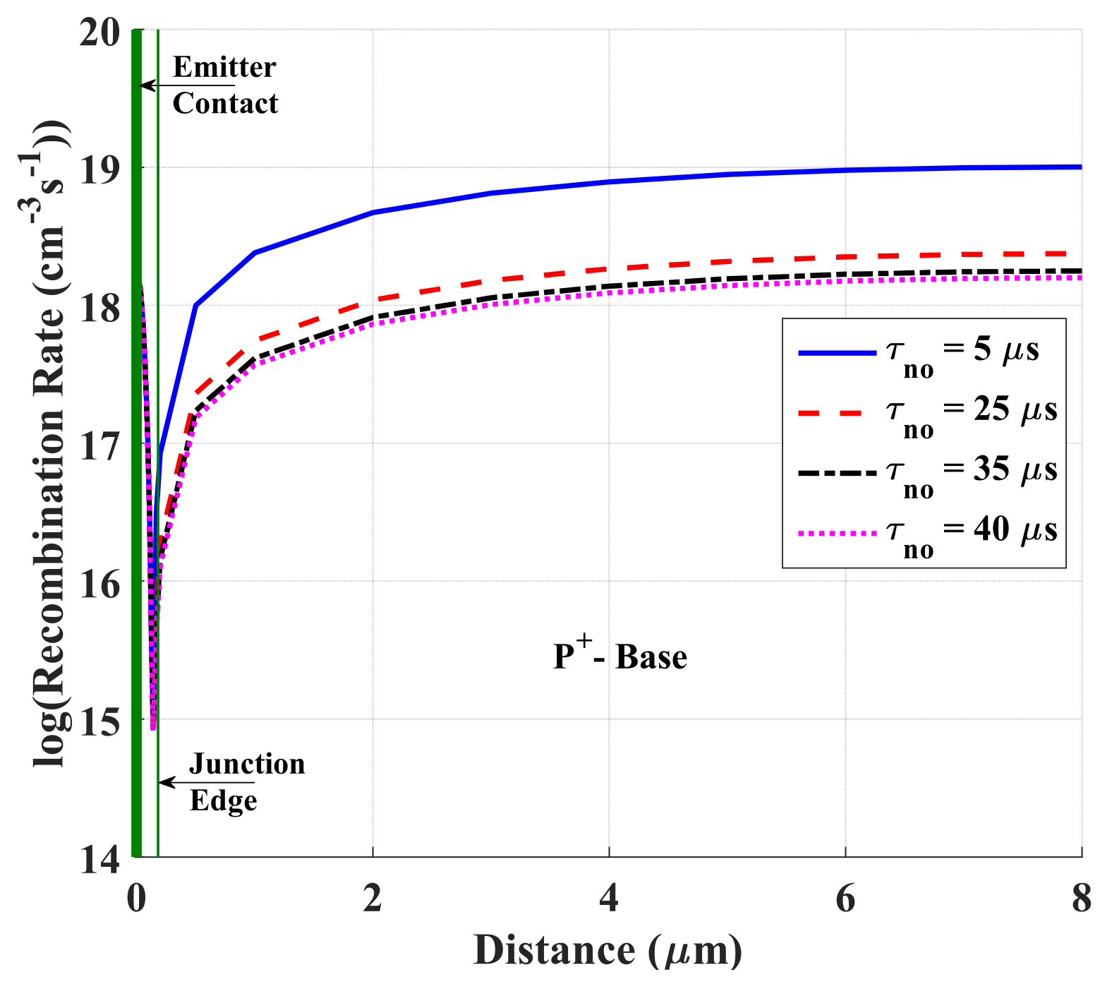
3.2. Effect of Different p+ Base Lifetime Variation

In this subsection, the p+ base bulk carrier lifetime is investigated in order to shed light on its influence on the performance of the proposed flipped microstructure. The bulk carrier lifetime is considered a key parameter that affects the recombination mechanism and hence the cell performance. The low-doped wafers using Czochralski or float zone processes are commonly used in the fabrication of Si solar cells to decrease the bulk recombination and hence improve the solar cell performance. In these wafers, the bulk lifetime of carriers is in the range of 50 µsec–500 µsec, but the cost of these wafers is still high, which impacts the overall cost of the SCs [41]. So, our design is based on using heavily doped low-cost Si wafers in the fabrication of our proposed flipped microstructure SC to overcome the challenge of the low lifetime values by generating the carriers vertically and laterally, collecting them through the small width of the cell.
The hole lifetime inside the p+- base was taken as a function of doping concentration, and it is expressed as
τ n = τ n o 1 + ( N p + , b a s e N r e f ) γ
where Nref = 5 × 1016 cm−3 and Np+,base = 1018 cm−3, and the constant γ is assumed to be 0.5 [20]. For the simulated heavily doped wafers, the bulk lifetime τno was assumed to be in the range of 1 µsec–40 µsec [42,43]. The influence of the bulk lifetime of carriers on the performance parameters of the flipped structure was examined and is presented in Figure 7, which demonstrates these parameters. As evident from the figure, the photovoltaic parameters are boosted by increasing the value of the lifetime up to about τno = 30 μs, resulting in an efficiency of about 16%. Beyond this value of base lifetime, the performance saturates. The increasing trend in the performance parameters of the cell is expected as the lifetime has a strong impact on the dark and illumination characteristics. It is clear from the figure that the increase in the bulk lifetime raises both the short-circuit current density and the open-circuit voltage. The boost in the Voc is due to the increase in the short-circuit current and the decrease in the reverse saturation current [18]. The saturation of the photovoltaic parameters of the flipped structure with the lifetime is because of the fact that as the lifetime increased, the diffusion length increases such that it becomes much greater than the base width. In this case, the current is controlled by the base width rather than the diffusion length, implying a constant efficiency for higher lifetime values. These results could also be explained by the recombination rate along the lateral distance of the cell structure for different values of base lifetime. The recombination rate, shown in Figure 8, decreases as the lifetime increases from 5 µs to 25 µs. When increasing the lifetime above 25 µs, the recombination rates have an insignificant change, which validates the findings in Figure 7.
Finally, we investigated the limit of the efficiency when non-radiative recombination losses were disabled. So, SRH and Auger recombination mechanisms were deactivated in the following simulation. Figure 9 displays the impact of the various recombination and BGN models on the J–V characteristics. The different cell performance metrics of the simulation cases are recorded in Table 3. τno is taken to be 30 μs when all models were included. As can be inferred from the figure, the Voc is enhanced and the Jsc slightly improves as well when the SRH recombination is neglected. On the other hand, Auger recombination has a similar impact when compared to the SRH model. An efficiency of 16.85% can be obtained when neglecting both SRH and Auger models. In addition, when deactivating the BGN model, an efficiency of 18.17% and a high Voc of 0.647 V are obtained. This means that the limiting factor of the Voc degradation comes mainly from the BGN effect. We are working on such impacts and the different ways to alleviate them to complete the design before fabrication of this type of cell.

4. Conclusions

In this work, we presented a proposed npn microstructure SC, whose configuration eliminates the shadowing effect that arises in the conventional npn structure. A simulation study was carried out using 2D TCAD SILVACO to inspect the performance of the cells under investigation. The cells were firstly implemented by a process simulator and, afterwards, a device simulator was incorporated to study the optical and electrical performance of the cells. It was found that the proposed flipped structure provided a higher efficiency than the conventional npn cell. This is mainly due to the design of the flipped structure, which facilitates the penetration of light across the whole upper surface.
Two main parameters were thoroughly investigated to determine their impact on the optical and electrical behavior of the npn microstructure cells. The parameters are the surface recombination velocity of the sidewall junction and the lifetime of the base region. It was realized that increasing surface recombination velocity and bulk lifetime significantly influenced the photovoltaic parameters. For SRV in the range from 1 to 104 cm/s, the efficiency did not change (at 15%). Thus, a good and clean oxide with low SRV did not degrade the structure performance. At an SRV of 105 cm/s, the efficiency appreciably decreased to 13.9%. For an SRV higher than 106 cm/s, the efficiency saturated at 13.3%. Concerning the base lifetime, τno, the efficiency increased with increasing τno, from 15% to 16% at τno above about 30 µsec. Beyond this value, the structure efficiency saturated at 16% with further increases in τno. Therefore, an efficiency of 16% could be obtained using practically feasible SRH lifetimes.
Moreover, the impact of SRH and Auger recombination mechanisms was studied to investigate the limit of the efficiency of such a proposed solar cell when neglecting non-radiative recombination mechanisms. This ideal situation gave an efficiency of about 16.85%. Finally, it was found that the main limiting factor for the open-circuit degradation came from the BGN effect. Texturing and anti-reflection coatings (ARCs) on the surface could be further studied to provide other possible paths for efficiency boosting. This simulation study is a proof of concept and can be extended to analyze large-area flipped npn structures, which can pave the way for high-efficiency low-cost SCs. In future work, we plan to fabricate a prototype in order to experimentally validate the results of the proposed design.

Author Contributions

M.S.S., A.Z., A.S., M.A., M.M.E. and R.A.R. had a role in the Conceptualization, Methodology, Writing—original draft, Validation and Investigation. M.S.S., A.Z., A.S., T.S.A., R.A.R. and M.T.A. contributed to Software, Formal analysis, Resources and Writing—review and editing. All authors have read and agreed to the published version of the manuscript.

Funding

This research was funded by the Scientific Research Deanship at the University of Ha’il—Saudi Arabia through the project number RD-21 009.

Data Availability Statement

Not applicable.

Acknowledgments

We appreciate Scientific Research Deanship at the University of Ha’il—Saudi Arabia funding for this research.

Conflicts of Interest

The authors declare no conflict of interest.

References

  1. Subramanian, M.; Nagarajan, B.; Ravichandran, A.; Subhash Betageri, V.; Thirunavukkarasu, G.S.; Jamei, E.; Seyedmahmoudian, M.; Stojcevski, A.; Mekhilef, S.; Minnam Reddy, V.R. Optimization of Effective Doping Concentration of Emitter for Ideal c-Si Solar Cell Device with PC1D Simulation. Crystals 2022, 12, 244. [Google Scholar] [CrossRef]
  2. Chigondo, F. From metallurgical-grade to solar-grade silicon: An overview. Silicon 2018, 10, 789–798. [Google Scholar] [CrossRef]
  3. Green, M.A.; Hishikawa, Y.; Warta, W.; Dunlop, E.D.; Levi, D.H.; Hohl-Ebinger, J.; Ho-Baillie, A.W. Solar cell efficiency tables (version 50). Prog. Photovolt. Res. Appl. 2017, 25, 668–676. [Google Scholar] [CrossRef] [Green Version]
  4. Zhou, L.; Xu, Y.; Tan, S.; Liu, M.; Wan, Y. Simulation of Amorphous Silicon Carbide Photonic Crystal Absorption Layer for Solar Cells. Crystals 2022, 12, 665. [Google Scholar] [CrossRef]
  5. Goodrich, A.; Hacke, P.; Wang, Q.; Sopori, B.; Margolis, R.; James, T.L.; Woodhouse, M. A wafer-based monocrystalline silicon photovoltaics road map: Utilizing known technology improvement opportunities for further reductions in manufacturing costs. Sol. Energy Mater. Sol. Cells 2013, 114, 110–135. [Google Scholar] [CrossRef]
  6. Kayes, B.M.; Atwater, H.A.; Lewis, N.S. Comparison of the device physics principles of planar and radial p-n junction nanorod solar cells. J. Appl. Phys. 2005, 97, 114302. [Google Scholar] [CrossRef]
  7. Garnett, E.; Yang, P. Light trapping in silicon nanowire solar cells. Nano Lett. 2010, 10, 1082–1087. [Google Scholar] [CrossRef]
  8. Lee, H.J. TCAD Simulation of Silicon Pillar Array Solar Cells. J. Semicond. Disp. Technol. 2017, 16, 65–69. [Google Scholar]
  9. Zhang, Y.; Liu, H. Nanowires for High-Efficiency, Low-Cost Solar Photovoltaics. Crystals 2019, 9, 87. [Google Scholar] [CrossRef] [Green Version]
  10. Elbersen, R.; Vijselaar, W.; Tiggelaar, R.M.; Gardeniers, H.; Huskens, J. Fabrication and doping methods for silicon nano-and micropillar arrays for solar-cell applications: A review. Adv. Mater. 2015, 27, 6781–6796. [Google Scholar] [CrossRef]
  11. Huang, B.R.; Yang, Y.K.; Lin, T.C.; Yang, W.L. A simple and low-cost technique for silicon nanowire arrays based solar cells. Sol. Energy Mater. Sol. Cells 2012, 98, 357–362. [Google Scholar] [CrossRef]
  12. Fan, Z.; Zhang, W.; Fu, Y.; Yan, L.; Ma, X. Facile synthesis of silicon micropillar arrays using extreme ultraviolet lithography and Ag-assisted chemical etching method. J. Phys. Chem. C 2016, 120, 6824–6834. [Google Scholar] [CrossRef]
  13. Dou, B.; Jia, R.; Li, H.; Chen, C.; Ding, W.; Meng, Y.; Xing, Z.; Liu, X.; Ye, T. High performance radial pn junction solar cell based on silicon nanopillar array with enhanced decoupling mechanism. Appl. Phys. Lett. 2012, 101, 183901. [Google Scholar] [CrossRef]
  14. Yang, T.C.; Lee, B.S.; Yen, T.J. Minimizing reflection losses from metallic electrodes and enhancing photovoltaic performance using the Si-micrograting solar cell with vertical sidewall electrodes. Appl. Phys. Lett. 2012, 101, 103902. [Google Scholar]
  15. Zhang, Y.; Fan, Z.; Zhang, W.; Ma, Q.; Jiang, Z.; Ma, D. High performance hybrid silicon micropillar solar cell based on light trapping characteristics of Cu nanoparticles. AIP Adv. 2018, 8, 055309. [Google Scholar] [CrossRef] [Green Version]
  16. Sahbel, A.; Hassan, N.; Abdelhameed, M.M.; Zekry, A. Experimental performance characterization of photovoltaic modules using DAQ. Energy Procedia 2013, 36, 323–332. [Google Scholar] [CrossRef] [Green Version]
  17. Putnam, M.C.; Boettcher, S.W.; Kelzenberg, M.D.; Turner-Evans, D.B.; Spurgeon, J.M.; Warren, E.L.; Briggs, R.M.; Lewis, N.S.; Atwater, H.A. Si microwire-array solar cells. Energy Environ. Sci. 2010, 3, 1037–1041. [Google Scholar] [CrossRef] [Green Version]
  18. Zekry, A.; Shaker, A.; Salem, M. Solar cells and arrays: Principles, analysis, and design. In Advances in Renewable Energies and Power Technologies, 1st ed.; Elsevier: Amsterdam, The Netherlands, 2018; Volume 1, pp. 3–56. [Google Scholar]
  19. Salem, M.S.; Alzahrani, A.J.; Ramadan, R.A.; Alanazi, A.; Shaker, A.; Abouelatta, M.; Zekry, A. Physically based analytical model of heavily doped silicon wafers based proposed solar cell microstructure. IEEE Access 2020, 8, 138898–138906. [Google Scholar] [CrossRef]
  20. Basyoni, M.S.; Zekry, A.; Shaker, A. Investigation of base high doping impact on the npn solar cell microstructure performance using physically based analytical model. IEEE Access 2021, 9, 16958–16966. [Google Scholar] [CrossRef]
  21. Salem, M.S.; Zekry, A.; Shaker, A.; Abouelatta, M. Design and simulation of proposed low cost solar cell structures based on heavily doped silicon wafers. In Proceedings of the 2016 IEEE 43rd Photovoltaic Specialists Conference (PVSC), Portland, OR, USA, 5–10 June 2016. [Google Scholar] [CrossRef]
  22. Salem, M.; Zekry, A.; Abouelatta, M.; Alshammari, M.T.; Alanazi, A.; Al-Dhlan, K.A.; Shaker, A. Influence of base doping level on the npn microstructure solar cell performance: A TCAD study. Opt. Mater. 2021, 121, 111501. [Google Scholar] [CrossRef]
  23. Salem, M.S.; Zekry, A.; Shaker, A.; Abouelatta, M.; Abdolkader, T.M. Performance enhancement of a proposed solar cell microstructure based on heavily doped silicon wafers. Semicond. Sci. Technol. 2019, 34, 035012. [Google Scholar] [CrossRef]
  24. Athena User’s Manual, Silvaco Inc., Santa Clara, USA. Available online: https://silvaco.com/products/tcad/process_simulation/athena/athena.html (accessed on 1 June 2022).
  25. Atlas User’s Manual, Silvaco Inc., Santa Clara, USA. Available online: https://silvaco.com/products/tcad/device_simulation/atlas/atlas.html (accessed on 1 June 2022).
  26. Del Alamo, J.; Swirhun, S.; Swanson, R.M. Simultaneous measurement of hole lifetime, hole mobility and bandgap narrowing in heavily doped n-type silicon. In Proceedings of the 1985 International Electron Devices Meeting, Washington, DC, USA, 1–4 December 1985. [Google Scholar] [CrossRef] [Green Version]
  27. Del Alamo, J.A.; Swanson, R.M. The physics and modeling of heavily doped emitters. IEEE Trans. Electron Devices 1984, 12131, 1878–1888. [Google Scholar] [CrossRef]
  28. Zekry, A. The dependence of diffusion length, lifetime and emitter Gummel-number on temperature and doping. Arch. Elektrotechnik 1992, 75, 147–154. [Google Scholar] [CrossRef]
  29. Zekry, A.; Gerlach, W. Reduction of the current gain of the npn transistor component of a thyristor due to the doping concentration of the p-base. IEEE Trans. Electron Devices 1988, 35, 365–372. [Google Scholar] [CrossRef]
  30. Zekry, A.; Shaker, A.; Ossaimee, M.; Salem, M.S.; Abouelatta, M. A comprehensive semi-analytical model of the polysilicon emitter contact in bipolar transistors. J. Comput. Electron. 2018, 17, 246–255. [Google Scholar] [CrossRef]
  31. Da, Y.; Xuan, Y. Role of surface recombination in affecting the efficiency of nanostructured thin-film solar cells. Opt. Express 2013, 21, A1065–A1077. [Google Scholar] [CrossRef] [PubMed]
  32. Morales-Vilches, A.B.; Voz, C.; Colina, M.; Munoz-Martin, D.; Martin, I.; Ortega, P.R.; Alcubilla, R. Study of the surface recombination velocity for ultraviolet and visible laser-fired contacts applied to silicon heterojunction solar cells. IEEE J. Photovolt. 2015, 5, 1006–1013. [Google Scholar] [CrossRef] [Green Version]
  33. Eberle, R.; Fell, A.; Niewelt, T.; Schindler, F.; Schubert, M.C. Analysis of temperature dependent surface recombination properties. AIP Conf. Proc. 2019, 2147, 140001. [Google Scholar] [CrossRef]
  34. Benmoussa, D. Study the effect of surface recombination velocity on performance of solar cells based SiGe. In Proceedings of the 4th International Conference on Automation, Control Engineering and Computer Science (ACECS-2017), Tangier, Morocco, 28–30 March 2017. [Google Scholar]
  35. Ali, K.; Khan, H.M.; Anmol, M.; Ahmad, I.A.; Farooq, W.A.; Al-Asbahi, B.A.; Ghaithan, H.M. Effect of surface recombination velocity (SRV) on the efficiency of silicon solar cell. J. Optoelectron. Adv. Mater. 2022, 22, 251–255. [Google Scholar]
  36. Stokkan, G.; Song, A.; Ryningen, B. Investigation of the Grain Boundary Character and Dislocation Density of Different Types of High Performance Multicrystalline Silicon. Crystals 2018, 8, 341. [Google Scholar] [CrossRef] [Green Version]
  37. Gatz, S.; Bothe, K.; Müller, J.; Dullweber, T.; Brendel, R. Analysis of local Al-doped back surface fields for high efficiency screen-printed solar cells. Energy Procedia 2011, 8, 318–323. [Google Scholar] [CrossRef] [Green Version]
  38. Khokhar, M.Q.; Hussain, S.Q.; Zahid, M.A.; Pham, D.P.; Cho, E.-C.; Yi, J. Numerical Simulation and Experiment of a High-Efficiency Tunnel Oxide Passivated Contact (TOPCon) Solar Cell Using a Crystalline Nanostructured Silicon-Based Layer. Appl. Sci. 2022, 12, 392. [Google Scholar] [CrossRef]
  39. Rahman, M.Z.; Khan, S.I. Advances in surface passivation of c-Si solar cells. Mater. Renew. Sustain. Energy 2012, 1, 1–11. [Google Scholar] [CrossRef]
  40. Ghannam, M.Y.; Kamal, H.A. Modeling surface recombination at the p-type Si/SiO2 interface via dangling bond amphoteric centers. Adv. Condens. Matter Phys. 2014, 2014, 857907. [Google Scholar] [CrossRef] [Green Version]
  41. Sze, S.M.; Lee, M.K. Semiconductor Devices: Physics and Technology. In Physics and Technology, 3rd ed.; Wiley Global Education: Hoboken, NJ, USA, 2012. [Google Scholar]
  42. Cuevas, A.; Macdonald, D. Measuring and interpreting the lifetime of silicon wafers. Sol. Energy 2004, 76, 255–262. [Google Scholar] [CrossRef]
  43. The Minority Carrier Lifetime in Silicon Wafer. Available online: https://meroli.web.cern.ch/lecture_lifetime.html (accessed on 15 November 2021).
Figure 1. Basic solar cell structures utilized in the study: (a) flipped npn microstructure and (b) conventional npn microstructure.
Crystals 12 00959 g001
Figure 2. The flipped structure using SILVACO Athena process simulator: (a) cross-sectional view for the whole cell showing the absolute net doping contours in cm−3, (b) a close view near the emitter region, (c) vertical cutline (perpendicular to the upper surface) showing the doping profile of the vertical pn junction and (d) lateral cutline showing the doping profile of right lateral pn junction.
Crystals 12 00959 g002aCrystals 12 00959 g002b
Figure 3. A comparison between the conventional npn and flipped structures: (a) external quantum efficiency (EQE) and (b) illuminated J–V characteristics.
Crystals 12 00959 g003
Figure 4. Comparison of J–V dark characteristics between the flipped and conventional structures.
Crystals 12 00959 g004
Figure 5. Photovoltaic parameter variation vs. surface recombination velocity.
Crystals 12 00959 g005
Figure 6. Impact of SRV on the reverse saturation current of the equivalent diode around Voc.
Crystals 12 00959 g006
Figure 7. Photovoltaic parameters variation vs. base lifetime.
Crystals 12 00959 g007
Figure 8. Recombination rate along the lateral distance of the flipped npn structure for different values of base lifetime.
Crystals 12 00959 g008
Figure 9. Illuminated J–V characteristics of the flipped npn structure for different models’ impact.
Crystals 12 00959 g009
Table 1. Summary of the photovoltaic parameters for the conventional npn and the flipped microstructures.
Jsc (mA/cm2)Voc (V)FF (%)PCE (%)
Conventional40.700.58080.3014.50
Flipped42.120.57381.7515.00
Table 2. Main parameters for dark characteristics for the conventional and the flipped microstructures. The analytical and TCAD values of the Voc are also listed.
Jo1 (A/cm2)n1Jo2 (A/cm2)n2Rs (mΩcm2)Voc,ana (mV)Voc,TCAD (mV)
Flipped2.46 × 10−91.6517.68 × 10−120.9986.780.5790.573
Conventional3.99 × 10−81.8476.02 × 10−130.90968.050.5860.580
Table 3. Photovoltaic parameters for the flipped microstructure when deactivating different models.
Jsc (mA/cm2)Voc (V)FF (%)PCE (%)
All models are enabled43.810.58882.0316.05
SRH: disabled44.130.59782.7216.55
SRH and Auger: disabled44.190.60582.8716.84
SRH, Auger and BGN: disabled44.190.64783.6718.17
Publisher’s Note: MDPI stays neutral with regard to jurisdictional claims in published maps and institutional affiliations.

