Article

Pulsed Sputtering Preparation of InGaN Multi-Color Cascaded LED Stacks for Large-Area Monolithic Integration of RGB LED Pixels

Institute of Industrial Science, The University of Tokyo, 4-6-1 Komaba, Meguro, Tokyo 153-8505, Japan
*
Author to whom correspondence should be addressed.
Crystals 2022, 12(4), 499; https://doi.org/10.3390/cryst12040499
Submission received: 10 March 2022 / Revised: 30 March 2022 / Accepted: 31 March 2022 / Published: 4 April 2022
(This article belongs to the Special Issue III-Nitride-Based Light-Emitting Devices)

Abstract

:
Micro-LEDs have been attracting attention as a potential candidate for the next generation of display technology. Here we demonstrate the feasibility of large-area monolithic integration of multi-color InGaN micro-LEDs via pulsed sputtering deposition (PSD) and a standard photolithographical technique. The PSD allows for sequential epitaxial growth of blue and green InGaN LED stacks connected with the GaN based tunneling junction. The tunneling junctions serve as protective layers on p-type GaN against the dry etching damage and hole injection layers in each blue and green emission InGaN active layer. The tunneling junction-connected multi-color InGaN LED stack contributes to the high-density and large-area monolithic integration of RGB micro-LEDs using standard photolithography and the ICP-dry etching method.

1. Introduction

Inorganic semiconductor-based micro-LED displays have attracted much attention as candidates for the next generation display system with superiorities over incumbent technologies such as OLEDs or liquid crystal displays [1,2,3,4]. Because of the superior nature of inorganic LEDs and the established semiconductor process technologies, micro-LED displays offer benefits over existing technologies, such as high pixel density, high brightness, high efficiency, and extended lifetime [3,4]. In particular, in recent years, there have been high expectations for applications in virtual reality (VR) and augmented reality (AR) displays. A highly integrated array of tens of millions of RGB-LEDs with a diameter of a few micrometers is required for high-resolution full-color VR/AR displays. InGaN blue/green LEDs and AlGaInP/AlGaAs red LEDs are used in contemporary micro-LED display technologies. As a result, this necessitates a time-consuming RGB LED chip assembling method known as pick-and-place or mass transfer [5,6,7]. The assembly process faces several problems in further scaling and integration, including low production yields and high manufacturing costs.
Monolithic epitaxial growth of InGaN RGB LED vertical stacks and subsequent photolithographic technique defining each RGB pixel array is one of the promising approaches for overcoming these obstacles. Micron meter-scale LED pixels appropriate for high-resolution and large-area AR/VR display applications can be defined all at once with the help of photolithography. Recent research works have shown the feasibility of the monolithic epitaxial integration of InGaN RGB-LEDs [8,9]. It has been demonstrated that the use of tunneling junction connected multiple LED stacks (cascaded LEDs) makes the independent operation of blue and green InGaN micro-LEDs possible [10]. The tunneling junction cascaded multi-color LED stack is quite attractive because it also offers current spreading and better ohmic contacts.
Epitaxial growth with MOCVD (Metalorganic Chemical Vapor Deposition) has conventionally been utilized for the manufacture of optical devices based on nitride semiconductors. However, for the preparation of cascaded multi-color LED displays, pulsed sputtering deposition (PSD) is the most appropriate epitaxial growth technique because it has the potential to enable low-temperature epitaxial growth of device-quality group III-nitride films on meter-by-meter sized substrates, resulting in high compatibility with the existing display industry [11]. In addition, PSD provides several advantages over conventional MOCVD, including an abrupt doping control, as-grown p-type conductivity without any dehydrogenation process, and the possibility of high-quality red emission InGaN growth [12,13,14]. Because the memory effect of Mg dopants, which is common for MOCVD growth [15,16], and thermal diffusion are effectively repressed, PSD is suitable for controlling the abrupt doping profile for Mg. As-grown p-type conductivity in GaN is caused by a low residual H impurity concentration below the SIMS detection limit. The PSD has a superior heavy doping capability for Si and Mg, which is required for low resistance tunneling connections [17,18,19,20].
In this article, we report on the first tunneling contact cascaded LEDs prepared with the use of PSD.

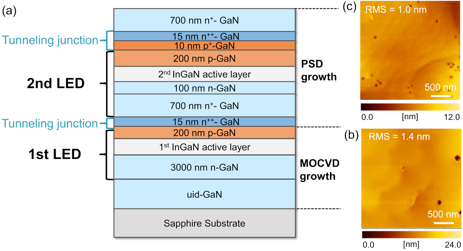
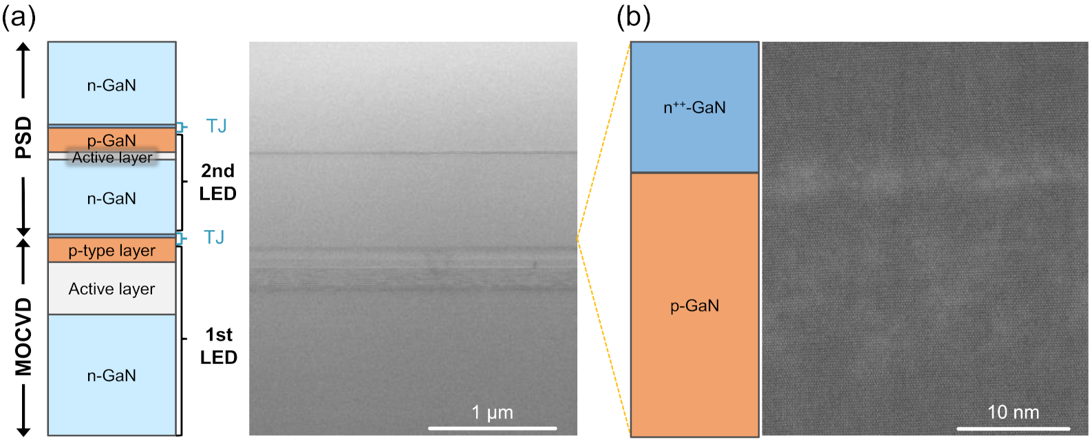
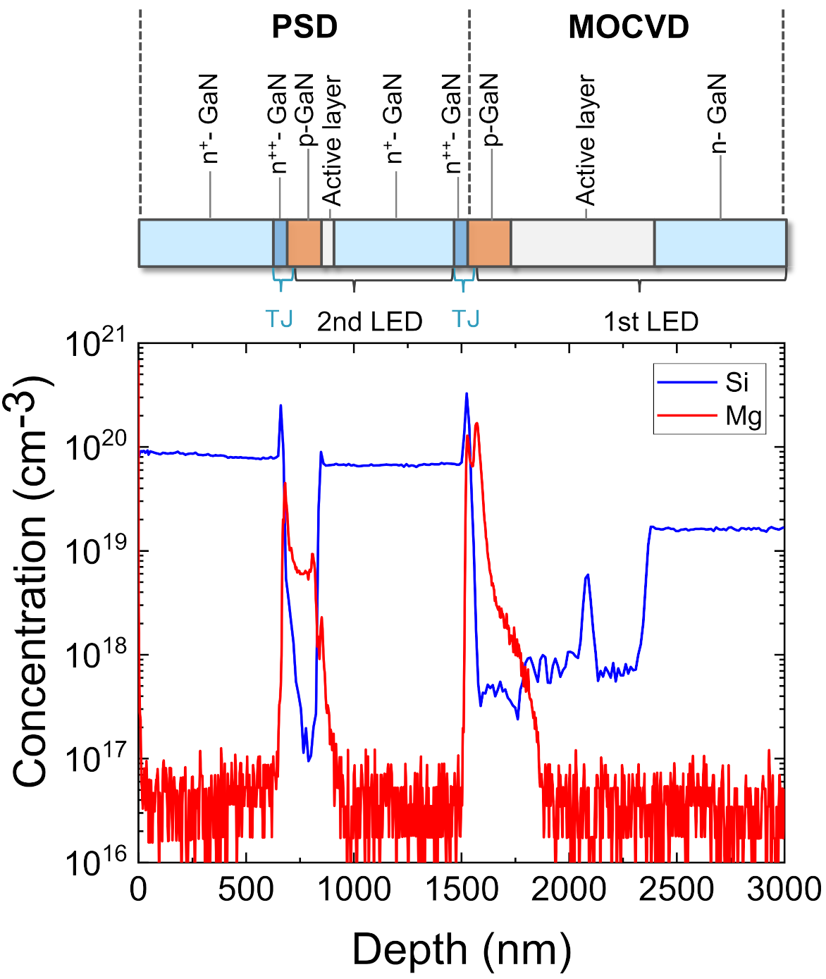
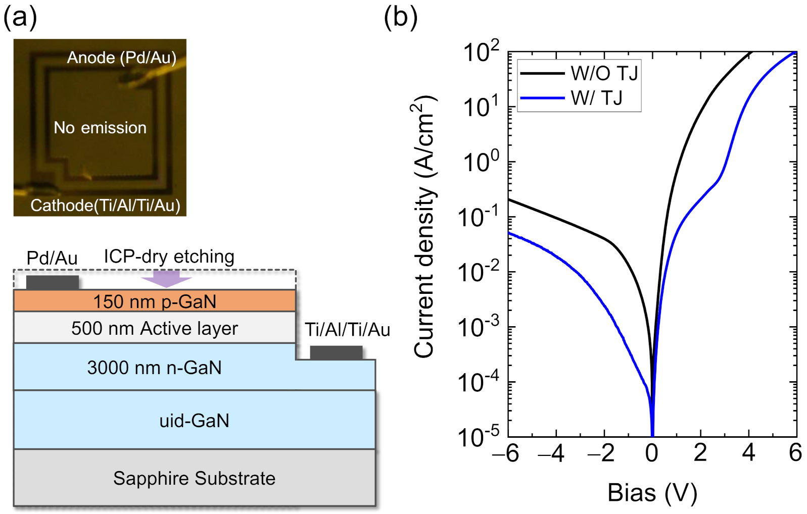
2. The Epitaxial Growth of the Tunneling Junction Connected InGaN LED Stack via PSD

Figure 1a depicts the cross-sectional schematic of a tunneling junction connected InGaN LED stack. The buried LED and top LED structures were named as the 1st and 2nd LED, respectively. Commercially available blue or green InGaN LED wafers were used as the starting materials, which were generated using a typical MOCVD process. In Figure 1b, hexagonal V-shaped pits can be found on the starting surface of p-type GaN wafers generated by MOCVD. The PSD was used to perform epitaxial growth in an Ar/N2 environment. The pulsed sputtering sources were operated at the discharged power ranging from 80 to 250 W. The growth rate of GaN was typically 0.5–1.5 μm/h. Growth temperature ranged from 500 °C to 700 °C. The epitaxial process started with the growth of a 15 nm-thick n++-GaN layer ([Si] = 2 × 1020 cm−3) and a 700 nm-thick n+-GaN layer ([Si] = 8 × 1019 cm−3) on the LED wafers. Sequentially, the 2nd LED structure was grown: 100 nm-thick n-GaN, 30 nm-thick InGaN active layer, 200-nm-thick p-GaN ([Mg]~3 × 1019 cm−3), and 10 nm-thick p+-GaN ([Mg]~1 × 1020 cm−3). The 2nd InGaN active layer consisted of a multiple quantum well structure with the In composition in the InGaN well of ca. 15%. A typical hole concentration of p-GaN grown under similar growth conditions was determined to be 1–2 × 1017 cm−3 from Hall effect measurements. Finally, the 2nd LED structure was capped with a 15 nm-thick n++-GaN layer ([Si] = 2 × 1020 cm−3) and a 700 nm-thick n+-GaN layer ([Si] = 8 × 1019 cm−3). The [Si] and [Mg] were controlled by changing the vapor fluxes from the solid-state pulsed sputtering sources. We also note that after the epitaxial process, no p-type activation annealing was performed. After the epitaxial process, the top surface of the tunneling junction of the second LED was atomically flat with a root mean square surface roughness of 1.0 nm as shown in Figure 1c. PSD-grown n+-GaN showed a relatively smoother surface morphology even with the high [Si] close to 1020 cm−3 compared to the case of MOCVD.
The microscopic structure of the tunneling junction connected InGaN LED stack is shown in cross-sectional transmission electron microscopy (TEM) (HD2700, Hitachi, Japan) images in Figure 2a,b. The Z-contrast image in Figure 2a confirmed the InGaN active layers in each LED as dark lines. Their interfaces remained abrupt after the epitaxial process, indicating negligible thermal damage to the InGaN active layers thanks to the low growth temperature of PSD. A low thermal budget epitaxial process is essential for integrating green or longer wavelength InGaN LEDs. The tunneling junction did not provide any contrast in Figure 2a. Even though the regrowth interface was not clearly visible in the high-resolution TEM image in Figure 2b, no additional structural defects, such as threading dislocations or stacking faults, were formed between the p-type GaN and n++-GaN layers.
SIMS measurements also revealed the Si and Mg doping profiles of the tunneling junction-connected LEDs stack. In Figure 3, one can see sharp rises of Si and Mg concentrations around 700 and 1500 nm-depth, respectively, which indicates the successful formation of tunneling junctions. The maximum [Mg] in the 1st and 2nd LED were estimated to be 1.7 × 1020 cm−3 and 5.0 × 1019 cm−3, respectively. In the n+- GaN layer, the Mg concentration in the p-GaN layer dropped to the background level. It is known that PSD allows for abrupt modulation of Mg concentration with a negligible thermal diffusion or memory effect, which is in stark contrast to conventional MOCVD [8]. In Figure 3, the overlaps between [Mg] and [Si] profiles at the tunneling junction interfaces may be attributed to the hexagonal V-shaped pits existing in the starting surface of p-type GaN. These findings suggest that PSD can be used to produce the tunneling junction and InGaN LEDs with abrupt doping profiles in a sequential manner.

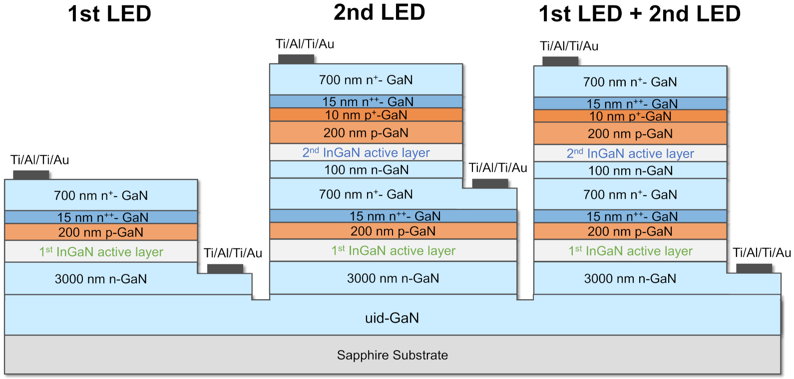
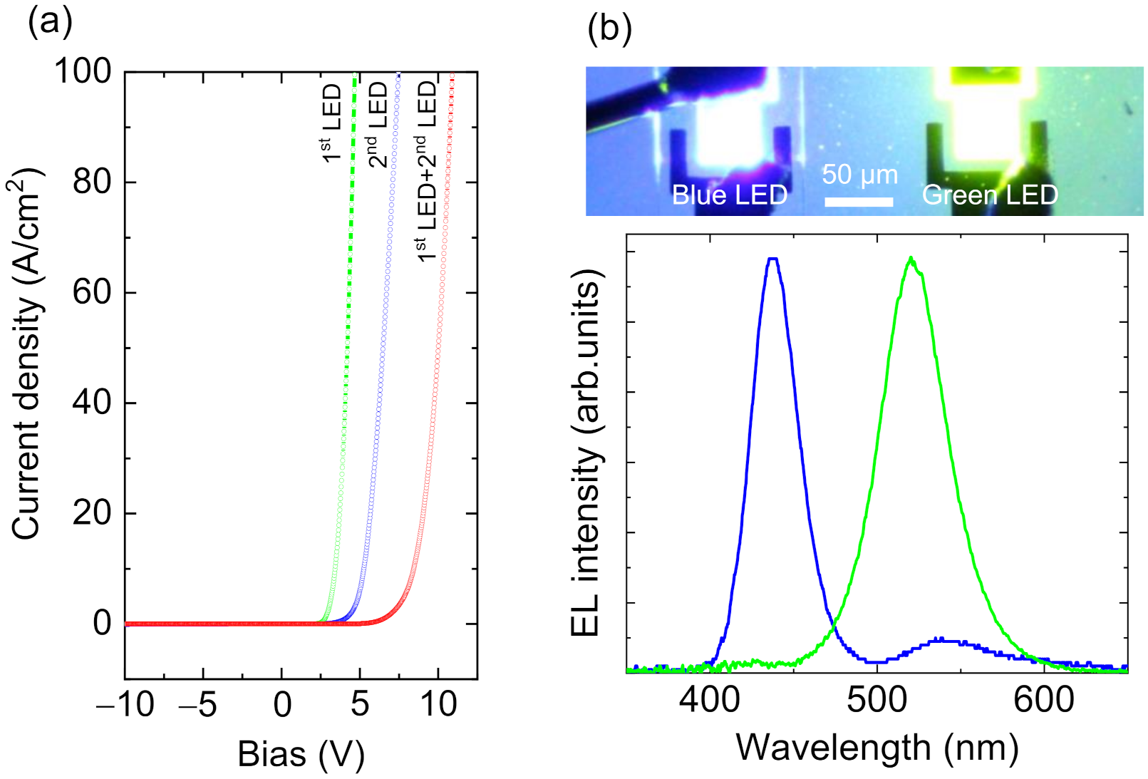
3. Monolithic Integration of Dual-Color LEDs

Conventional photolithography defined the LED mesa and ohmic electrode patterns. The dry etching was performed using an ICP-RIE plasma etching system (RIE-101PHi, Samco inc., Kyoto, Japan) with the ICP and RF power of 80 and 30 W, yielding the etching rate of 80 nm/min for GaN. The etching rate determined the ething depth for the formation of anode and cathode electrodes and device isolation. The n-type and p-type ohmic contacts were Ti/Al/Ti/Au (20/40/20/40 nm) and Pd/Au (50/50 nm) metal stacks, respectively. Using UHV e-beam deposition equipment, all electrode metals were deposited. Figure 4 shows the monolithic integration of dual-color LEDs in cross-section.
The deep etching to the uid-GaN layer electrically isolated each LED device. The cathode electrodes of the 1st LED and the 2nd LED were deposited on the bottom n-type GaN and n+-GaN layers of the tunneling junctions, respectively.
The anode electrodes were deposited on n+-GaN of the tunneling junctions. To investigate the validity of the tunneling junction for avoiding the dry etching damage against the p-type GaN layer, we also prepared the reference LED with the anode electrode on the etched p-type GaN layer, as shown in Figure 5a.
Figure 5b shows current density-voltage (J-V) characteristics of the reference LED and the 1st LED with the tunneling junction. The reference LED exhibited poor rectifying characteristics with a higher reverse leakage current density and lower turn-on voltage than a typical p-n junction and consequently yielded no light emission. The poor rectifying behavior can be explained by the n-type Schottky behavior with the Schottky barrier height of 0.59 eV and the ideality factor of 8.27, respectively. These values are similar to those found in defective Pd/n-type GaN. The dry etching method damaged the p-type GaN layer, making hole injection into the InGaN active layer difficult. The lower bias power ICP-dry etching possibly reduced the etching damage to the p-type GaN layer [21]. Although the post-etching treatment, including N2 plasma exposure, [22] NH3/N2 annealing, [23] and wet etching [24] also removed the surface damage of the p-type GaN, the properties of p-type contacts could not be totally recovered.
In the case of micro-LEDs, these treatments may unintentionally cause extra damage. As a result, more advancements in p-type ohmic behavior and in-plane homogeneity will be required for micro-LED applications.
The tunneling junction-contact LEDs, on the other hand, had excellent rectifying characteristics, with a reasonable turn-on voltage of roughly 4 V at 20 A/cm2 and a lower leakage current, and they produced clear light emission from the InGaN active layers, as described below. The tunneling junction contacts will be a promising way to uniformly make low-resistive anode contacts for the micro-LED applications because the epitaxial process can mainly determine the anode properties.
Figure 6a summarizes the current-voltage characteristics of the monolithically integrated 1st LED, 2nd LED, and 1st LED + 2nd LED, respectively. In Figure 6a, the LED mesa size was 90 × 90 μm2. The LED devices all have distinct rectifying properties. The forward voltage of the buried 1st LED was 3.71 V at 20 A/cm2. The voltage penalty across the tunneling junction was well suppressed, and less than 1 V, while state-of-the-art InGaN LEDs with ITO contacts operate at roughly 3 V forward voltage. This is attributed to the high Mg and Si doping levels with the abrupt doping profile in the tunneling junction. The 2nd LED yielded a relatively higher forward voltage of 5.67 V at 20 A/cm2. We believe that the high forward voltage can be explained by the high sheet resistance of the bottom n+-GaN.We need further optimization in the film thickness and doping profiles. The 1st LED + 2nd LED yielded a reasonable forward voltage of 9.05 V at 20 A/cm2, almost equal to the sum of the forward voltages of the 1st LED and 2nd LED. The EL spectra and optical microscope image of blue and green LEDs on the same wafer with a 50 μm squared emission area are shown in Figure 6b. The uniform blue and green emissions were observed, and their light intensities can be controlled separately. The full width at half maximum values were 33 and 45 nm for blue and green emissions in Figure 6b. The buried 1st LED worked well without significant damage even after ICP-dry etching. Additionally, the low-temperature PSD approach may be preferable for creating high In composition red emission InGaN LEDs, as it has already demonstrated high brightness InGaN LEDs with a 633 nm emission wavelength [12]. Thus, the PSD technique will be quite attractive for the sequential growth of the RGB InGaN LED stack with the tunneling junction. This clearly indicates the feasibility of the high-density monolithic integration of RGB micro-LEDs using standard photolithography and the ICP-dry etching process.

4. Conclusions

Using a multi-color InGaN LED stack with a GaN tunneling homojunction, we were able to show monolithic integration of InGaN blue and green micro-LEDs. The tunneling junctions served as dry etching protection and hole injection layers in each blue and green emission InGaN active layer on p-type GaN. The cross-sectional TEM and SIMS measurements revealed that the PSD technique enabled the sequential epitaxial growth of the tunneling junction-connected blue and green LEDs with abrupt doping profiles and high-structural quality. The multi-color InGaN LED stack will contribute to the high-density monolithic integration of RGB micro-LEDs using standard photolithography and the ICP-dry etching process.

Author Contributions

Conceptualization, K.U. and H.F.; methodology, S.M.; formal analysis, S.M. and K.U.; investigation, S.M. and K.U.; writing—original draft preparation, S.M. and K.U.; writing—review and editing, A.K. and H.F.; supervision, H.F. All authors have read and agreed to the published version of the manuscript.

Funding

This research was funded by the A-STEP from JST Grant no JPMJTR201D.

Data Availability Statement

Not applicable.

Conflicts of Interest

The authors declare no conflict of interest. The funders had no role in the design of the study; in the collection, analyses, or interpretation of data; in the writing of the manuscript; or in the decision to publish the results.

References

  1. Wu, T.; Sher, C.-W.; Lin, Y.; Lee, C.-F.; Liang, S.; Lu, Y.; Chen, S.-W.H.; Guo, W.; Kuo, H.C.; Chen, Z. Mini-LED and Micro-LED: Promising Candidates for the Next Generation Display Technology. Appl. Sci. 2018, 8, 1557. [Google Scholar] [CrossRef] [Green Version]
  2. Wu, Y.; Ma, J.; Su, P.; Zhang, L.; Xia, B. Full-Color Realization of Micro-LED Displays. Nanomaterials 2020, 10, 2482. [Google Scholar] [CrossRef] [PubMed]
  3. Ding, K.; Avrutin, V.; Izyumskaya, N.; Özgür, Ü.; Morkoç, H. Micro-LEDs, a Manufacturability Perspective. Appl. Sci. 2019, 9, 1206. [Google Scholar] [CrossRef] [Green Version]
  4. Zhang, K.; Peng, D.; Lau, K.M.; Liu, Z. Fully-integrated active matrix programmable UV and blue micro LED display system-on-panel (SoP). J. SID 2019, 25, 240–248. [Google Scholar] [CrossRef]
  5. Choi, M.; Jang, B.; Lee, W.; Lee, S.; Kim, T.W.; Lee, H.-J.; Kim, J.-H.; Ahn, J.-H. Stretchable Active Matrix Inorganic Light-Emitting Diode Display Enabled by Overlay-Aligned Roll-Transfer Printing. Adv. Funct. Mater. 2017, 27, 1606005. [Google Scholar] [CrossRef]
  6. Geum, D.-M.; Kim, S.K.; Kang, C.-M.; Moon, S.-H.; Kyhm, J.; Han, J.; Lee, D.-S.; Kim, S. Strategy toward the fabrication of ultrahigh-resolution micro-LED displays by bonding-interface-engineered vertical stacking and surface passivation. Nanoscale 2019, 11, 23139–23148. [Google Scholar] [CrossRef] [PubMed]
  7. Kim, B.H.; Nam, S.; Oh, N.; Cho, S.-Y.; Yu, K.J.; Lee, C.H.; Zhang, J.; Deshpande, K.; Trefonas, P.; Kim, J.-H.; et al. Multilayer Transfer Printing for Pixelated, Multicolor Quantum Dot Light-Emitting Diodes. ACS Nano 2016, 10, 4920–4925. [Google Scholar] [CrossRef] [PubMed]
  8. Robin, Y.; Hemeret, F.; D’Inca, G.; Pristovsek, M.; Trassoudaine, A.; Amano, H. Monolithic integration of tricolor micro-LEDs and color mixing investigation by analog and digital dimming. Jpn. J. Appl. Phys. 2019, 58, SCCC06. [Google Scholar] [CrossRef]
  9. Ichikawa, S.; Shiomi, K.; Morikawa, T.; Timmerman, D.; Sasaki, Y.; Tatebayashi, J.; Fujiwara, Y. Eu-doped GaN and InGaN monolithically stacked full-color LEDs with a wide color gamut. Appl. Phys. Express 2021, 14, 031008. [Google Scholar] [CrossRef]
  10. Li, P.; Li, H.; Yao, Y.; Zhang, H.; Lynsky, C.; Qwah, K.S.; Speck, J.S.; Nakamura, S.; DenBaars, S.P. Demonstration of high efficiency cascaded blue and green micro-light-emitting diodes with independent junction control. Appl. Phys. Lett. 2021, 118, 261104. [Google Scholar] [CrossRef]
  11. Sato, K.; Ohta, J.; Inoue, S.; Kobayashi, A.; Fujioka, H. Room-Temperature Epitaxial Growth of High Quality AlN on SiC by Pulsed Sputtering Deposition. Appl. Phys. Express 2009, 2, 011003. [Google Scholar] [CrossRef]
  12. Nakamura, E.; Ueno, K.; Ohta, J.; Fujioka, H.; Oshima, M. Dramatic reduction in process temperature of InGaN-based light-emitting diodes by pulsed sputtering growth technique. Appl. Phys. Lett. 2014, 104, 051121. [Google Scholar] [CrossRef]
  13. Arakawa, Y.; Ueno, K.; Kobayashi, A.; Ohta, J.; Fujioka, H. High hole mobility p-type GaN with low residual hydrogen concentration prepared by pulsed sputtering. APL Mater. 2016, 4, 086103. [Google Scholar] [CrossRef] [Green Version]
  14. Shon, J.W.; Ohta, J.; Ueno, K.; Kobayashi, A.; Fujioka, H. Fabrication of full-color InGaN-based light-emitting diodes on amorphous substrates by pulsed sputtering. Sci. Rep. 2014, 4, 5325. [Google Scholar] [CrossRef] [Green Version]
  15. Ohba, Y.; Hatano, A. A study on strong memory effects for Mg doping in GaN metalorganic chemical vapor deposition. J. Cryst. Growth 1994, 145, 214–218. [Google Scholar] [CrossRef]
  16. Xing, H.; Green, D.S.; Yu, H.; Mates, T.; Kozodoy, P.; Keller, S.; DenBaars, S.P.; Mishra, U.K. Memory Effect and Redistribution of Mg into Sequentially Regrown GaN Layer by Metalorganic Chemical Vapor Deposition. Jpn. J. Appl. Phys. 2003, 42, 50–53. [Google Scholar] [CrossRef]
  17. Ueno, K.; Fudetani, T.; Arakawa, Y.; Kobayashi, A.; Ohta, J.; Fujioka, H. Electron transport properties of degenerate n-type GaN prepared by pulsed sputtering. APL Mater. 2017, 5, 126102. [Google Scholar] [CrossRef]
  18. Fudetani, T.; Ueno, K.; Kobayashi, A.; Fujioka, H. Wide range doping controllability of p-type GaN films prepared via pulsed sputtering. Appl. Phys. Lett. 2019, 114, 032102. [Google Scholar] [CrossRef]
  19. Fudetani, T.; Ueno, K.; Kobayashi, A.; Fujioka, H. Heavily Si-doped pulsed sputtering deposited GaN for tunneling junction contacts in UV-A light emitting diodes. Appl. Phys. Lett. 2021, 118, 072101. [Google Scholar] [CrossRef]
  20. Morikawa, S.; Ueno, K.; Kobayashi, A.; Fujioka, H. Pulsed sputtering growth of heavily Si-doped GaN (2021) for tunneling junction contacts on semipolar InGaN (2021) LEDs. Appl. Phys. Express 2021, 14, 051011. [Google Scholar] [CrossRef]
  21. Kumabe, T.; Ando, Y.; Watanabe, H.; Deki, M.; Tanaka, A.; Nitta, S.; Honda, Y.; Amano, H. Etching-induced damage in heavily Mg-doped p-type GaN and its suppression by low-bias-power inductively coupled plasma-reactive ion etching. Jpn. J. Appl. Phys. 2021, 60, SBBD03. [Google Scholar] [CrossRef]
  22. Kent, D.G.; Lee, K.P.; Zhang, A.P.; Luo, B.; Overberg, M.E.; Abernathy, C.R.; Ren, F.; Mackenzie, K.D.; Pearton, S.J.; Nakagawa, Y. Electrical effects of N2 plasma exposure on dry-etch damage in p- and n-GaN Schottky diodes. Solid-State Electron. 2001, 45, 1837–1842. [Google Scholar] [CrossRef]
  23. Moon, Y.-T.; Kim, D.-J.; Park, J.-S.; Oh, J.-T.; Lee, J.-M.; Park, S.-J. Recovery of dry-etch-induced surface damage on Mg-doped GaN by NH3 ambient thermal annealing. J. Vac. Sci. Technol. B 2004, 22, 489. [Google Scholar] [CrossRef]
  24. Lee, J.-M.; Lee, K.-S.; Park, S.-J. Removal of dry etch damage in p-type GaN by wet etching of sacrificial oxide layer. J. Vac. Sci. Technol. B 2004, 22, 479. [Google Scholar] [CrossRef]
Figure 1. (a) A cross-sectional schematic of a tunneling junction connected InGaN LEDs stack with the tunneling junctions. The starting material was an MOCVD-grown LED wafer, and the regrowth interface was located between the 15 nm-thick n++-GaN and 200 nm-thick p-type GaN. (b,c) AFM images of a starting p-type GaN surface and a top surface of the LED.
Crystals 12 00499 g001
Figure 2. (a) A cross-sectional Z-contrast TEM image of the LED stack. (b) a high-resolution-TEM image of the regrowth interface.
Crystals 12 00499 g002
Figure 3. SIMS profile of Si and Mg in the LED stack with the tunneling junctions.
Crystals 12 00499 g003
Figure 4. A cross-sectional schematic of the monolithic integration of dual-color LEDs and their anode and cathode arrangements.
Crystals 12 00499 g004
Figure 5. (a) A cross-sectional schematic and optical microscope image of the p-type GaN surface etched LED (reference). (b) Current density–voltage characteristics of the reference LED and tunneling junction (TJ) contact LED.
Crystals 12 00499 g005
Figure 6. (a) Current density–voltage characteristics of the monolithically integrated 1st LED, 2nd LED, and 1st LED +2nd LED, respectively. (b) An optical microscope image and EL spectra of the monolithically integrated 1st and 2nd LEDs.
Crystals 12 00499 g006
Publisher’s Note: MDPI stays neutral with regard to jurisdictional claims in published maps and institutional affiliations.

